by Vijay Choudhary and Sourav Sen, Texas Instruments
In part one of this blog series on Fly-Buck™ topology, we introduced the reason and the idea for a secondary compensation loop for the isolated side. In this entry, we will review the compensation circuit and present the improvement in the secondary side regulation.

Figure 1. The Fly-Buck converter with feedback compensation circuit on the secondary output
Figure 1 shows the complete compensation circuit in conjunction with the original LM5017 application circuit. The external compensation circuit includes an opto-coupler for feedback isolation and the LM431A, a shunt regulator used as an error amplifier with appreciable gain at lower frequencies [3]. The feedback circuit includes a typical Type I compensation network (C1, R1) which determines the cut-off frequency. The Type I compensation also ensures a high DC gain reducing the low frequency DC regulation error. As the phototransistor in the opto-coupler switches on, the effective feedback ratio at the primary output drops.
The modified circuit with the correct circuit parameters is shown in Figure 2. With the addition of the compensation circuit, the apparent value of the resistor divider ratio (RFB2/RFB1) changes during the operation. The high side feedback resistor RFB2 needs to be updated in order to re-adjust the primary output voltage to a set point slightly above the nominal 12V.
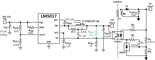
Figure 2. The LM5017 based Fly-Buck converter circuit with opto-coupler based regulation circuit
As is evident in Figures 3a, 4a and 5a (dotted line), the opto-coupler based secondary side regulation circuit considerably improves the secondary regulation when compared to the uncompensated secondary output. The negative gradient in the secondary output voltage with load as seen in the original LM5017 circuit has been significantly reduced using this circuit. Also the secondary output voltage remains closely regulated to nominal 5V with increase in the input voltage. However, this improved regulation on the secondary side comes at the expense of marginal drop in primary output regulation as the fundamental relationship between the two outputs is still dictated by the power stage. Figures 3b, 4band5b show the effective primary voltage regulation in this new configuration and how they compare with respect to the original circuit.
| |
Figure 3a. Secondary Side Load Regulation
| Figure 3b. Primary Side Load Regulation
|
| |
Figure 4a. Secondary Side load Regulation
| Figure 4b. Primary Side load Regulation
|
Figure 5a. Secondary Side load Regulation
| Figure 5b. Primary Side load Regulation
|


The main purpose of the inclusion of this isolated feedback compensation circuit in the original Fly-Buck converter was to improve the secondary output voltage regulation over the load and the input voltage range. It is evident from the results above, this isolated compensation circuit helps in maintaining the isolated output voltage regulation considerably.
References
- Texas Instruments “Designing an isolated buck (Fly-Buck) converter”
LM5017: 100V, 600mA Constant On-Time Synchronous Buck Regulator
“Designing with TL431” by Ray Ridley
- Texas Instruments Engineer It video, "How to use Fly-Buck DC/DC converter topology"