Have you been experiencing problems with fluctuations in capacitance measurements within your sensor system? There are several explanations for these fluctuations, but the most common root cause is external parasitic capacitance interference. This interference, for example unintentional hand proximity or EMI from the surrounding area, requires attention and should be addressed in system design, since it can significantly reduce system reliability and sensitivity. Fortunately, there are ways to help mitigate these factors so that they do not affect capacitance-measurement readings; one of those ways is through active shielding. The FDC1004 features active shield drivers that can reduce interference and help focus the sensing field of a capacitive sensor.
Imagine a wire connected to one of the channel inputs of the FDC1004. As your hand approaches the wire and comes into contact with it, your hand forms a closed loop with the signal on the wire, since the human body acts as a grounded source. If your hand is not the intended target, it is considered a parasitic capacitance. The solution: an active shield wrapped around the wire. The shield driver is an active signal output that is driven at the same voltage potential (same waveform) as the sensor input, so there is no potential difference – and thus no capacitance – between the shield and sensor input. Any external interference will couple the shield signal with minimal interaction with the sensor signal. Figure 1 shows how shielding the signal line from sensor to the FDC1004 will reduce any interferers from affecting capacitance measurements.
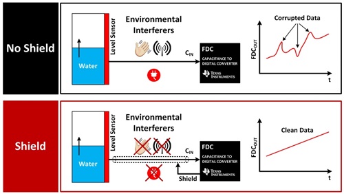
Figure 1: Shield versus no shield comparison
There are several benefits to using a shield in capacitive-sensing applications:
- It directs and focuses the sensing zone to a particular area.
- It reduces and eliminates parasitic capacitances and interferers.
- It eliminates temperature variation effects on the ground plane.
Directivity with a shield
With no shield, the sensor, CH, detects objects above and below the sensor. Depending on the application, detection above and below may not be acceptable and can misrepresent the capacitance measurements relative to a target. By using a shield sensor underneath the CH and GND electrodes, the field lines below are essentially blocked; only the top field lines have a defined path. The example shown in Figure 2 is somewhat simplified and does not include fringing effects.
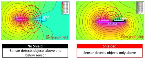
Figure 2: Electric field lines between CH and GND
Parasitic capacitance and interferers
Good system-level design principles require a ground plane to help reduce noise and increase signal integrity. For capacitive-sensing applications, a ground plane becomes an issue because it creates a termination source for electric field lines, even though the ground plane is not where the intended sensing area should be. If the printed circuit board (PCB) stack up is similar to that shown in Figure 3, fringing effects will occur and cause the measurements to include the capacitance path from the sensor to the ground plane. This large ground parasitic capacitance can be reduced significantly with a shield plane between the sensor and ground plane.
In an ideal case, the shield will eliminate all influence from the ground plane; but because of fringing effects, a small parasitic ground capacitance amount will still exist in the measurements. The shield size would have to be much greater than the size of the sensor and ground plane so that the field lines on the edges are much weaker compared to the overall capacitance measurement.
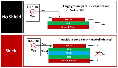
Figure 3: Ground-plane effects with and without shielding
Temperature effects on ground planes
Temperature is a factor that causes the parasitic ground plane capacitance to vary in addition to the initial parasitic capacitance offset it introduces into the measurements. This is seen as an offset that is time-varying. These variations from temperature are caused by expansion and contraction of the ground plane. Inserting a shield plane between the sensor and ground plane helps mitigate the influence of the parasitic ground plane capacitance from the measurements.
Typical implementation with the FDC1004
The FDC1004 has the capability to drive a 400pF load on the shield driver pins. Any load greater than 400pF will cause the shield to not function properly and effectively. Pairing the input channels with a shield depends on the mode of operation. In single-ended mode, CIN1 through CIN4 can be paired with either SHLD1 or SHLD2, because the two shield pins are shorted internally. For differential mode, Table 1 lists the in-phase conditions.
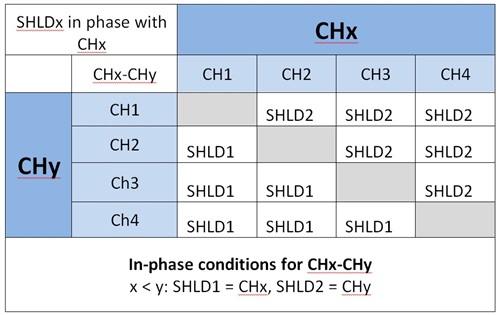
Table 1: Channel and shield pairing for differential mode
For example, if the FDC1004 is configured so that CH1-CH4, CH1 would be in-phase and paired with SHLD1, while CH4 would be in-phase and paired with SHLD2.
Stay tuned for part 2 of this series to learn more about shield sensor design, and how the size and placement of the shield in relation to the sensor electrode affects sensor performance.
Additional resources:
- Download the FDC1004 data sheet.
- Experience capacitive-sensing technology firsthand with the FDC1004EVM, which you can order today for US$29.
- Check out the newest TI Designs reference design for capacitive-based human-proximity detection for system wake-up and interrupt.
- Search for answers and get help with your designs in the TI E2E™ Community Capacitive Sensing forum.