The recent introduction of power gallium nitride (GaN) and silicon carbide (SiC) field-effect transistors (FETs) into the market are opening up many possibilities for system improvements. As power-conversion designers, we are always in need for lower losses, not only to reduce the cost of heat sinks and fans but also because of the energy-saving possibilities that provide rapid payback for designing-in higher-cost wide-band gap devices.
Radio frequency (RF) engineers were among the first to embrace GaN as a way to meet higher power, higher linearity and higher RF amplifier efficiency targets for cellular base stations and other high power RF systems such as radar. RF analysis tools such as Smith charts and spectrum analysis provides key learnings to gain insight into ways to improve higher-frequency power-conversion designs including GaN. The most common use of Smith charts is to understand how transmission lines change the impedance of PCB traces and passive elements.
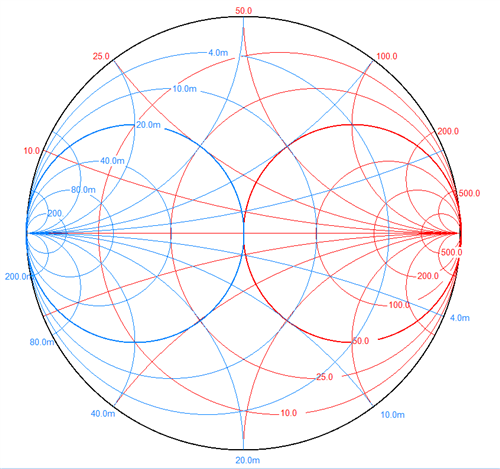
Figure 1 Smith Chart
PCB Parasitics
RF engineers don’t just try to minimize board parasitics, they typically design the parasitics to be a specific value, and take into account the transmission line effects that cause the parasitics to be a function of frequency. For example, it is common to implement broad band capacitors as open circuited stubs and inductors as short circuited stubs. It is also common for passive devices such as surface mount resistors to be modeled for their equivalent capacitance to ground from each pad and their series inductances due to their length that turn the resistor into a lossy low pass filter.
Smith Charts 101
Smith charts are graphical aids especially used by electrical engineers specializing in RF. Open circuits plot as the right most point. Short circuits plot as the left most point. All other impedances are plotted based on their real and imaginary values as a ratio to the impedance of the signal path they are propagating in, for example 50ohms. In a 50 ohm system, an ideal 50ohm resistor would be plotted as a point in the center of the Smith chart. Adding a length of transmission line (e.g. PCB trace) between an open or short circuit causes the impedance looking into the transmission line to change. If the length of line is 0.25 wavelengths long, the open will look like a short or the short will look like an open.
There are many free online Smith chart tools such as the one from Fritz Dellsperger from Bern University. This tool allows simple circuits to be plotted and analyzed as a function of frequency. I also like the smartphone app from Seward Salvage. Just search “Seward Salvage” in the app store.
PCB Trace Lengths
The length of the PCB trace between the measurement point and the open or short must be converted into a fractional wavelength to see how much the open or short is rotated (clockwise) around the Smith chart. The wavelength of a signal at a specific frequency follows the relationship:
lamda = c/f. Where c is the speed of light in the medium and f is the frequency
For Air, c = ~3x10^8 meters/sec. For PCB materials, such as FR-4, the wavelengths will be shorter as a function of the square root of the dielectric constant. For striplines in FR-4 material, the dielectric constant is approximately 4 and the wavelengths are half of what they are in air. This also means that an impedance is rotated twice as much for a PCB transmission line than what it would be in an air filled waveguide.
Wavelength (medium) = Wavelength in air/SQRT(dielectric constant)
RF designers must take into account the length of a signal path and the impedances as a function of frequency along that path to determine how their circuits will perform. Power conversion designers have felt that their frequencies are low enough to ignore transmission line effects but that is no longer true with GaN based power designs with switching frequencies above 10MHz and with harmonic content above 100MHz. For example, I used a network analyzer to measure the impedance of a top layer trace, approximately 5mm by 6mm that was 5mils above a ground plane on layer 2. Figure 2 shows the impedance verses frequency, from 5MHz to 1GHz.

Figure 2 5mm x 6mm Trace Capacitance and Resonance
Note that an ideal capacitor would plot only along the negative imaginary (bottom half) outer circle of the smith chart, starting at the highest impedance point where the capacitor has an infinite impedance and then move along clockwise toward the low impedance side as frequency is increased. At 100MHz this pcb pad/trace is 2.9 – 189.2j ohms. The self-resonance loop near the stop frequency of 1GHz is due to the size of capacitor and transmission line effects.
Figure 3 is the parasitic inductance of a 0.10 ohm SMT resistor used to measure current.
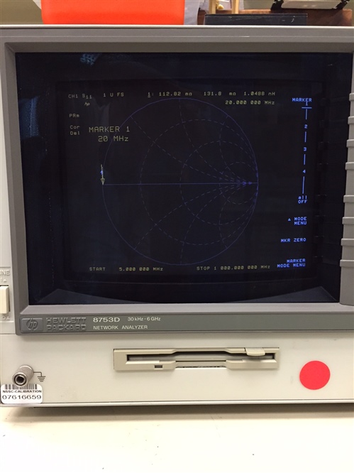
Figure 3 SMT Resistor plus parasitic series inductance
Ideally this resistor would have no inductance and simply plot as a point just inside the 0 ohm, left most point on the Smith chart at 0.1ohm. Note that as the measurement frequency increases, the inductance of the resistor starts to dominate. At 20MHz, the resistor measures 0.112 + .132j and the inductance is determined to be ~1nH. At 500MHz, the bandwidth needed to accurately see a current rise time of 3.5ns possible with this GaN FET, the inductance impedance is ~3ohms, 30x larger than the DC value.
To learn more about TI’s GaN technology visit our GaN solutions website. Stay tuned for future Power House blogs on designing with GaN using RF power techniques.