What is eUSB2?
As applications like smartphones and tablets continue to pack more and more components into smaller form factors, it’s essential that interfaces shrink as well. However, the continued shrinking of system-on-chip (SoC) node size has led to a thinner gate oxide that can only support lower voltages. For devices relying on USB 2.0 interfaces, this trend can lead to complicated design challenges for advanced process nodes.
When process nodes reach 7 nm, quantum effects begin impacting high-signaling-voltage inputs/outputs (I/Os) such as 3.3 V and can no longer be easily supported. Many device-to-device interfaces already support low signaling voltages, but USB 2.0 still requires a 3.3-V I/O voltage to operate.
To address this challenge, the USB Implementers Forum released the embedded USB2 (eUSB2) specification in 2018. This specification addresses issues related to USB 2.0 interface controller integration with advanced SoC process nodes by enabling USB 2.0 to operate at I/O voltages of 1 V or 1.2 V instead of 3.3 V. eUSB2 can enable smaller, more power-efficient SoCs, in turn enabling process nodes to continue to scale while increasing performance in applications such as smartphones, tablets and notebooks.
Differences between USB 2.0 and eUSB2
USB 2.0 has been the most successful wired interface in the past 20 years, and almost all SoCs today are equipped with the USB 2.0 interface. USB standards evolution kept the original 3.3-V I/O USB 1.0 interface intact for backward compatibility, helping enable wider adoption and a larger ecosystem while also preserving device interoperability.
As process nodes approach 5 nm, the manufacturing cost to maintain USB 2.0 3.3-V I/O signaling has grown exponentially. eUSB2 addresses the I/O voltage gap as a physical layer supplement to the USB 2.0 specification so that designers can integrate the eUSB2 interface at the device level while leveraging and reusing the USB 2.0 interface at the system level.
eUSB2 can support onboard inter-device connectivity through direct connections as well as exposed connector interfaces through an eUSB2-to-USB 2.0 repeater to perform level shifting, as illustrated in Figure 1.
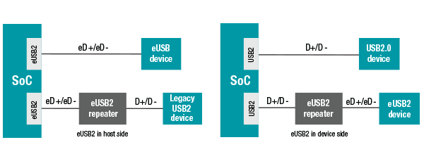
Figure 1: eUSB2 applications
While USB 2.0 can continue to be integrated into SoCs with process nodes 7 nm and above, eUSB2 is a good fit for SoCs when process nodes are 5 nm and below. eUSB2 can also be integrated into other devices, also shown in Figure 1, to easily interconnect with SoCs as a device-to-device interface. USB 2.0 will continue serving as the standard connector interface.
eUSB2 allows significant I/O power reduction and improves power efficiency, while enabling process nodes to continue to scale. Table 1 shows the feature differences between USB 2.0 and eUSB2.
Feature | USB 2.0 | eUSB2 |
Signal interface | D+, D- | eD+, eD- |
I/O voltage | 3.3 V | 1 V or 1.2 V |
Supported data rate | Low speed: 1.5Mbps Full speed: 12Mbps High speed: 480Mbps | Low speed: 1.5Mbps Full speed: 12Mbps High speed: 480Mbps |
Connectivity | Inter-device Out of the box | Inter-device Out of the box with USB 2.0 through repeater |
Table 1: Differences between USB 2.0 and eUSB2
The future of eUSB2
eUSB2 is a good fit for device-to-device communications with smaller I/O voltages, as the system power is greatly reduced.
Designers of small-size electronics can adopt eUSB2 in system designs when using cutting-edge SoCs with 5-nm process nodes and beyond, while continuing to benefit from the simplicity, ease of design and omnipresence of the USB 2.0 interface.
In our next technical article on the eUSB2 specification, we will discuss design considerations for eUSB2 repeaters and how to implement them.