Quantcast
Channel: TI E2E support forums
Viewing all 4543 articles
Browse latest View live

Designing an EMC-compliant interface to motor position encoders – Part 1

$
0
0

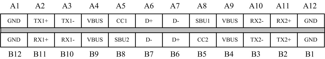
Motor position encoders are widely used in industrial motor control applications such as servo drives, robotics, machine tools, printing machines, textile machines and elevators. Interfacing these encoders to the rest of your system can raise some tricky electromagnetic compatibility (EMC) issues. To help you meet these challenges, I’ll begin this series with an overview of the various types of motor position encoders and their interface, and the rest of the series will dive into designing an industrial EMC-compliant interface to each of the various motor position encoder types.

Depending on the industrial drive’s application, the required position/angle resolution can vary from a few bits to 25 bits and beyond. Some drive applications even require the number of angular turns. The mounting distance from the frequency inverter to the position encoder can vary from very short – a few meters in multi-axis drives – to 100m and beyond. Due to that long distance the electrical interface needs to be designed for robust data transmission with high immunity against electromagnetic fields, common mode voltage, impulse noise, etc.

Figure 1 shows several types of linear or angle position feedback encoders for industrial applications.

Figure 1: Position feedback encoders and their corresponding interfaces

There are two types of position encoders: incremental and absolute. Incremental encoders provide information on the incremental position or angle change. After power-up they do not provide the absolute position, although it is still possible to obtain through the index signal after one mechanical revolution. Absolute encoders always provide the absolute mechanical position.

Incremental encoders exhibit three differential signals: A, B and Z. A and B encode the incremental position change. The position resolution depends on the line count of the incremental encoder. A typical range is 50 to 10,000 line counts per revolution. Z typically occurs once per revolution and is a “home index” used to derive the absolute position.

Incremental encoder interfaces are either digital pulse train with transistor-transistor logic (TTL)- or high-threshold logic (HTL)-compatible digital output levels or analog sine/cosine outputs with 1Vpp or 11µApp amplitude. Encoders with analog outputs are often referred to as sin/cos encoders and allow for much higher resolution than encoders with TTL/HTL output because you can interpolate its position within one line count by using the inverse tangent function with the measured sine and cosine signals. This interpolation can increase the resolution by as much as 16 bits, with a possible total resolution of 25 bits or more. The frequency of the output signals is proportional to the line count of the selected encoder times the rotation speed.

Absolute position feedback encoders provide the absolute position with up to 25-bit resolution and more. Their electrical interface has evolved from a hybrid analog and digital protocol-based serial interface to a pure digital protocol-based serial interface. The standards for serial communication are typically vendor-specific and leverage RS-485 or RS-422 differential signaling with bidirectional data transfer. For example, EnDat 2.2 not only transmits the absolute position, but also allows readout from and writing to the encoder’s internal memory. You can select the type of data transmitted – absolute position, turns, temperature, further parameters, diagnostics – through mode commands that the subsequent electronics, often referred to as the EnDat 2.2 master, send to the EnDat2.2 encoder.

Pure digital serial protocol-based standards like EnDat2.2, BiSS® and HIPERFACE DSL® are capable of compensating for the propagation delay and supporting communication over a cable length of up to 100m. Pure digital protocols have a constant clock frequency, which does not change with rotation speed. For most protocols, you can select the clock frequency/baud rate to adapt to external factors, like cable length.

Encoders with a mixed analog and digital communication interface or a pure digital communication interface typically have a vendor-specific supply-voltage range. Table 1 is an overview of widely used encoder standards.

Table 1: Position encoder interface standards and supply voltages

When interfacing any of these encoders to a frequency inverter for closed-loop control, the position interface module incorporates the following functional blocks, as shown in Figure 2:

  • A physical analog or digital interface.
  • Electromagnetic compatibility (EMC) according to IEC 61800-3.
  • A power supply.
  • Signal processing for position decoding and/or a digital protocol master.

Figure 2: Simplified block diagram of a position feedback interface module on an industrial drive/frequency inverter

 Incremental digital HTL/TTL encoders and absolute digital encoders with the RS-485 or 422 interface require a lower hardware interface effort, while analog sin/cos encoders require an analog signal chain with a dual analog-to-digital converter. You need to design the physical interface to meet EMC immunity requirements like electrostatic discharge (ESD), electrical fast transient (EFT) bursts and surge with levels defined in IEC61800-3:

  • ESD: ±4kV, direct-contact discharge or ±8kV air discharge.
  • EFT: ±2kV, 5kHz, through a capacitive coupling clamp.
  • Surge: ±1kV, 2-Ω source impedance, coupling through the cable shield.

TTL/HTL encoders require the lowest signal-processing effort, requiring only a directional quadrature pulse counter. Incremental sin/cos encoders require signal processing to calculate the inverse tangent for interpolation in addition to the quadrature counter. Digital serial interface protocol-based standards require high signal-processing effort and are typically implemented on FPGAs, or more recently on innovative processors like the Sitara™ AM437x, which leverages the programmable real-time unit subsystem and industrial communication subsystem (PRU-ICSS) peripheral.

In the next installment of this series, my colleagues and I will take a closer look at each encoder interface and provide details on how to implement an industrial, EMC-compliant interface to a BiSS-C position encoder/BiSS-C master interface.

If you’re ready to start designing, check out these TI Designs reference designs for interfaces to EnDat2.2, BiSS, HIPERFACE DSL and sin/cos encoders. Please go to ti.com/tidesigns and search for the corresponding encoder standard.

If you would like to see this series touch on specific topics related to position encoder interface design, please log in to post a comment below.

Additional resources


Automotive Surround View Technology trends

$
0
0

When driving cars in computer games, we can typically get a view of the car and its surroundings as if we are looking at the car from the top or from the back. These views help us better drive the car by showing us what surrounds us. Unfortunately, we do not have the same views when driving in real life, but this is changing nowadays with the introduction of automotive surround view systems (also called “birds eye view” or “around view”). Surround view is an advanced driver assistance systems (ADAS) technology that shows to the driver a birds-eye 360-degree camera view of the car and its surroundings in real-time in order to enable safer driving at low speeds such as parking. Since there is really no actual camera in real life looking at the car from the top, the birds-eye view that is shown to the driver is in fact a virtual view that is synthesized from a composite of 4 to 6 fish-eye cameras that are installed around the car as shown in the example below.


As surround view systems are incorporated into more cars, we are observing several key trends. One is the trend towards higher visual quality. Early surround view systems were using low-resolution cameras and did not attempt to apply seamless stitching. Instead they put black bars in places where the different camera views border each other. More advanced systems seamlessly stitch the views to make the birds-eye view more realistic. An example is shown above from TI’s TDA2x based surround view system that includes seamless stitching. Achieving seamless stitching requires advanced geometric and photometric alignment algorithms that TI’s Digital Signal Processors (DSPs) can implement efficiently. (Read here for more information) Visual quality can be further improved by applying Wide Dynamic Range (WDR) imaging algorithms in the surround view system. Automotive use cases include many situations where there is significant lighting difference on different sides of the car, such as when a car is coming out of a parking garage. In these situations, WDR imaging can help create a surround view output where both dark and bright regions are clearly visible. Variants of TI’s TDA3x processor has WDR imaging capabilities, which can be applied to surround view systems.

Another potential improvement in visual quality is video noise filtering. When surround view systems are used at night time, the camera output will typically contain high levels of noise due to low light. Advanced video noise filtering algorithms can be applied to reduce the level of noise and improve surround view quality. The TDA3x processor provides high quality video noise filters.

Surround view systems typically include only the birds-eye camera view looking at the car from the top. One interesting additional capability is to enable the camera view point to dynamically change so that the driver can look at the car from various directions and choose the direction that they prefer most. This is accomplished with the help of GPU-based rendering. The TDA2x System-on-Chip (SoC) has an SGX544 graphics engine that can be used to implement 3D surround view with dynamic free camera view point.

There are other areas of improvement for advanced surround view systems, such as refining the rendering of objects that are in the close vicinity of the car. Surround view systems currently stretch these objects while rendering them. Sometimes when these objects are close to stitching boundaries, ghosting artifacts are created. More advanced algorithms will reduce these distortions in the future and make the output video look more realistic.

In addition to the visual quality improvement trends discussed above, there is yet another set of interesting developments where intelligent algorithms are implemented on top of surround view to detect certain events and alert the driver in case of an emergency. Pedestrians and other objects around the car can lead to collusions and are important for the driver to be aware of. Vision algorithms that are analyzing the surround view video can detect these objects and overlay warnings on the surround view display to focus the attention of the driver. These algorithms could also fuse additional sensors (such as ultrasonic) with the surround view camera system to achieve higher robustness. In the future, we can expect surround view systems to even achieve autonomous driving at low speeds.

Tinker Maker DIY

$
0
0

TI AvatarAt TI, we celebrate the makers and hobbyists who enjoy creating and innovating on their own time. In our ongoing DIY with TI series, we share their incredible Do It Yourself inventions using TI technology.

Will Cooper has the best of two worlds.

A tinkerer at heart, Will enjoys making useful gadgets with TI parts.

“It’s cool that I work for a company where I can make stuff for myself and it ends up being beneficial to my real job,” he said.

Some of his creations are simple. He assembled a remote control using an MSP430™ LaunchPad microcontroller (MCU) and a battery booster pack with infrared functionality to manage decorative LED light strings in his backyard. A Wi-Fi plug controlled by his smart phone enables him to turn interior lamps on and off so it looks like his house is occupied when nobody is home. Will showed the remote control at our DIY with TI Showcase Event in May.

Some of his projects are more complex. He has built LaunchPad-based robots with sensors that detect when a person or object is in its way. He and some colleagues also built an energy-harvesting system that demonstrates the use of sensors powered by sources as diverse as indoor light, wind and temperature.

Now the Dallas-based MSP430 MCU product marketing engineer is pondering his next DIY project. He enjoys backyard gardening, so he may build a microcontroller-based watering system to keep his vegetables and herbs alive during the hot Texas summers.

“I want to make life easier, and that leads me to build stuff at home all the time,” he said. “People love it when you can demonstrate applications they’re interested in, such as energy harvesting and wireless. The value of our products is really clear in these types of applications.”

Designing a digital power supply: How to write firmware

$
0
0

In part 1 of this blog series, I talked about how to design a digital power supply using Texas Instruments' UCD3138 as an example and focusing on the hardware design. In this installment, I’ll explain how to write firmware to make it work.

Firmware

Unlike analog power-converter design, which controls everything by hardware, the firmware is the “soul” of digital control; almost all major functions are implemented through code. Because the code is subject to real-time constraints with limited central processing unit (CPU) bandwidth, it is very important to have a well-organized firmware structure.

You can divide the tasks the CPU handles into two categories: time-critical and non-time-critical. Time-critical tasks include ADC measurements, loop control, system protection and state machine. Non-time-critical tasks usually include PMBus/universal asynchronous receiver/transmitter (UART) communication, fault logging, etc.

Based on these two categories, the firmware is divided into two major parts: the interrupt loop, which handles time-critical tasks; and the background loop, which handles non-time-critical tasks. Figure 1 illustrates the firmware structure:

Figure 1: Firmware structure

The block diagram of the background loop is simple: After system initialization, the CPU goes into an infinite loop. All non-time-critical tasks are performed in this loop. In the meantime, a timer generates interrupts with a fixed frequency. If at any time there is an interrupt, the CPU will stop what it is doing, store all related data and jump to the interrupt routine. Once the interrupt routine is complete, the CPU goes back to the background loop and continues from where it stopped.

The interrupt loop is more complicated. It measures the ADC inputs, controls the converter and is responsible for system protection. The key part of the interrupt loop is the state machine, which indicates the current state of the converter, what the converter needs to do in this state, and what the converter should do next. Figure 2 is a simple state machine example:

 Figure 2: State machine diagram

The CPU continues monitoring the input voltage. Once the input voltage goes above a pre-defined threshold, the converter turns on and begins to perform a soft start, while the output voltage linearly increases until it reaches a set point. Once the output voltage reaches that set point, the converter enters regulation mode, where it will stay until a fault occurs or it is commanded to turn off. If at any time a fault occurs, the converter will shut down and latch, unless commanded to restart.

Using the GUI

TI’s Fusion Digital Power Designer graphical user interface (GUI) facilitates UCD3138-controlled power-converter designs. By talking to the GUI through the PMBus, you can monitor the power-supply operating status, configure operation parameters and tune the control loop on the fly.

The GUI supports the most popular topologies, including PFC, LLC and phase-shifted full bridge. Different topologies will have different GUI interfaces. A setup ID in the firmware tells the GUI what the topology is so that it will open an interface to accommodate that topology. Figure 3 shows a GUI for a PFC converter:

Figure 3: UCD3138 GUI

Communication

A digital controller can monitor the converter and communicate with the host; in turn, the host can send commands to the converter to perform tasks such as output-voltage adjustment, power-on sequencing, remote on/off control, etc. In an isolated AC/DC application, a PFC is followed by an isolated DC/DC converter, UART is used for communication between PFC and DC/DC, and PMBus is used for communication between DC/DC and load/host, as shown in Figure 4.

 Figure 4: Communication in an isolated AC/DC system

For UART communication between PFC and DC/DC, there is no industry standard protocol at this time; however, the UCD3138 team has developed a complete primary/secondary communication protocol example ready for use. 

Hopefully by now you get a rough idea of how to design a digital controlled power supply. Although the design example I gave in this series is based on a boost converter, the same design principle applies to other topologies. The power stage is the same compared to analog solutions, but the control implementation is different: one is implemented through the code and can be dynamic changed, while the other is implemented hardware and is fixed. Firmware development takes lots of work in digital converter designs. Writing code may be a challenge for analog engineers, but once you get used to it, you will enjoy the advantages of digital power.

Additional Resources


Get started with the Educational BoosterPack MII

$
0
0

It is finally here! The Educational BoosterPack Mark II is the ideal BoosterPack for beginners looking to develop on microcontrollers (MCUs) and seasoned engineers who would like to explore the possibilities of TI MCUs for their next project. This BoosterPack provides the ultimate combination of inputs and outputs to expand the functionality of TI microcontrollers! The best part is we are offering theEducational BoosterPack MK II for this month only at US$29.99!

What's Included:

  • TI OPT3001 Light Sensor
  • TI TMP006 Temperature Sensor
  • Servo Motor Connector
  • 3-Axis Accelerometer
  • User Push Buttons
  • RGB Multi-color LED
  • Buzzer
  • 40-pin Stackable BoosterPack Connector
  • Color TFT LCD Display
  • Microphone
  • 2-Axis Joystick with Pushbutton


Order Today!

There are two options to buy the Educational BoosterPack MKII on the TI Store. The development board is available standalone, or in a bundle with the MSP432 Launchpad Development Kit. 

Avoid noise pollution in Hi-Fi systems with low noise power supply

$
0
0

High-fidelity (Hi-Fi) audio is a combination pure and harmonic sounds, so captivating that the listener is transported to a higher level of bliss and happiness. Thanks to technological advances the Hi-Fi experience is becoming widely available in portable devices like smart phones, tablets, media players and many more.

Figure 1 shows the main components that contribute to Hi-Fi audio; at the center of the diagram is the power management (PM) system. The PM directly affects every component in the audio signal chain. It’s essential to design a low-noise and low-ripple power supply to avoid unwanted signals that can affect the noise-sensitive components in the systems. 

Figure 1: Main components for Hi-Fi audio systems

High efficiency switch-type regulators could be used to power the system; however, the switching and ripple noise common to switch-type regulators may harm the signal integrity and create an audible pop or hum noise in the audio system. External filters can reduce the noise but increase complexity, cost and total solution size. Luckily, noise reduction and ripple rejection can be obtained with an easy-to-implement, small size and low cost linear regulator (LDO). LDOs keep the output voltage regulated with line and load variations even under very small input/output voltage differences (also known as dropout voltage).  

Detailed information and test data of a low-noise power supply for Hi-Fi applications can be obtained by looking at one example in a reference design for audio applications, TIDA-00571. Figure 2 from the TIDA-00571 design compares the noise density of the TPS62203 buck regulator with the LP5907 LDO; the buck converter has a notorious spike and subsequent harmonics within the audio bandwidth of 20 Hz and 20 kHz. 

Figure 3 compares the LP5907 (LDO) and TPS65130 EVM (buck-boost).It is notorious that the white noise is higher in the buck-boost device, adding an LDO after the buck-boost will greatly improve the noise over a wide range of frequencies.

Figure 2: Comparison between TPS62203 EVM and LP5907

Figure 3: Noise comparison between TPS65130 Buck-Boost and LP5907

Figure 4 compares the output ripple of the boost converter with the quiet output voltage of the LP5907. The notorious 45mV in the blue trace is nonexistent at the LDO output. 

As we have seen LDOs offer considerable benefits over switching topologies for noise-sensitive applications, especially in the low frequencies range like Hi-Fi audio systems.

For other design advice related to LDOs, check out other blog posts.

Additional resources:

How to easily move from USB 2.0 to USB Type-C

$
0
0

Are you excited about moving your USB 2.0 (or USB 1.1) application – such as a flash drive, charger, power adapter, external drive or hard drive – to the USB Type-C reversible connector? Here’s a guide to easily migrate your USB 2.0 Type-A, Type-B or micro-A peripheral, host or On-The-Go (OTG) design to Type-C.

The connector

Figure 1 shows the receptacle pin assignment for supporting a full-featured Type-C cable that supports both USB 2.0 and USB 3.1.

Figure 1: USB Type-C full-featured receptacle pin map (front view)

 When migrating from a USB 2.0 product to a Type-C product, you will not need the USB 3.1 signals, so leave them unconnected (electrically isolated) on the printed circuit board (PCB). Figure 2 shows the USB 3.1 contacts as no-connects (NC) in a Type-C receptacle.

Figure 2: Receptacle pin map with USB Type-C USB 2.0 (front view)

 The pin map in Figure 2 has two sets of D+ and D- contacts. These two sets of pins do not imply that there are two independent USB 2.0 paths. In fact, a USB Type-C cable has only one wire for D+ and one wire for D-. The purpose of these two sets of D+/D- contacts is to support the “flippable” feature. Products should connect both the two D+ contacts together as well as the two D- contacts together on their PCB. When tying these contacts together on the PCB, creating a stub is unavoidable. As such, be careful that the stub length does not exceed 2.5mm. Otherwise, you may notice signal-integrity issues on the USB 2.0 interface.

Noticeably absent from the USB Type-C receptacle is the ID pin of the older Type-A and Type-B connectors. The determination of host or peripheral functionality is handled differently in Type-C using the configuration channel (CC) pins. The CC pins perform the same functions that the ID pin previously performed; they indicate the role of equipment as host, peripheral or both. The CC pins also detect if the connection is being made or if it is broken; and a few additional things not required when implementing USB 2.0 on Type-C.

One-chip solution

You can transition a USB 2.0 host, peripheral or OTG product that uses a micro-A/B receptacle to a USB Type-C receptacle with one device – the TUSB320. This family of devices can function as an upstream-facing port (UFP), downstream-facing port (DFP) or a dual-role port (DRP) product based on a pin or value of an I2C register. The device handles all aspects of the USB Type-C connection process, (including the CC pins that mirror the micro-A/B ID pin behavior) for easy determination of the DFP or UFP role.

When connected as a peripheral (UFP), the TUSB320 indicates the VBUS current provided by the attached host through either I2C registers or general-purpose input/output (GPIO) pins. When connected as a DFP, these devices advertise VBUS current to the attached peripheral.

Are you moving to USB Type-C? If so, what application are you migrating? Let us know in the comments section below.

Additional resources

Read TI’s white paper


Meet the new Educational BoosterPack MKII for TI LaunchPad development kits

$
0
0
  • 2-axis analog joystick w/digital input
  • 3-axis analog accelerometer
  • TI TMP006 Infrared Contact-less temperature sensor
  • TI OPT3001 Ambient Light Sensor
  • 128x128 back-lit color LCD
  • RGB multi-color LED
  • Microphone
  • Buzzer
  • 2 digital pushbuttons
  • Alligator clips that can turn external items into digital inputs


This BoosterPack pairs well with many of our 40-pin LaunchPad™ development kits, including the MSP-EXP430F5529LPMSP-EXP432P401REK-TM4C123GXL and others. 

See the Educational BoosterPack MKII in action:

(Please visit the site to view this video)

(Please visit the site to view this video)

LINKS TO GET STARTED!

  • You can get the Educational BoosterPack MKII here
  • Download the Energia software examples here!
  • Get the MSP432 LaunchPad software examples here!

High cell battery packs fuel new applications and extend time between charges

$
0
0

We can all remember a time when we’ve really needed to use an electronic device, only to find out the battery is dead. For years, our portable electronics have been limited by battery life and battery size. As the cost of Lithium-ion batteries continues to decrease and the charge density increases, longer lasting and exciting portable applications will emerge. As applications begin to trend toward using these high-cell battery packs, designers will be faced with converting higher voltages to voltages that are practical for compact electronic circuitry, while overcoming the challenges of transient effects and variation in battery voltage.

Examples include drones, vacuum robots, power tools, and E-bikes. Developers are trending toward using higher cell battery packs to increase battery life between charging. Currently, flight time for drones is limited to roughly 25 minutes, and E-bikes can travel a maximum of 50 miles on a single charge. This battery life will increase as smaller, higher voltage batteries are used.

One commonality between all of these applications is a motor, which can have adverse transient effects on the supply voltage such as motor kick-back and inductive spikes that can be as high as twice the input voltage. These higher voltages can damage the system power solution and other internal circuitry if the input voltage range is not rated accordingly. If the motor abruptly stops or slows down, a negative current is pumped into the supply causing the supply voltage to increase. In the figure below, channel 1 shows the supply current, channel 2 shows the supply voltage, and channel 3 shows the motor speed.

Figure 1: Supply pumping due to slowing of a motor.

As the motor slows down, the supply voltage significantly increases. If the DC/DC converter off the battery is not rated to operate at a higher voltage, this will damage the system power solution and potentially downstream components.

When designing a system, selecting a DC/DC converter that supports a wide range of input voltages can minimize, and often eliminate, the need for external transient protection circuitry. This not only simplifies the design, but also significantly decreases the solution size. Systems using DC/DC converters that can operate at higher voltages are able to withstand an increase in supply voltage and maintain voltage regulation at the output. TI’s LM5000 family of devices is a well-suited solution with an input voltage rated for up to 42V/65V to handle transients for 12V/24V systems. For example, the LM5007 and LM25011 are a good fit for protecting against a brief increase in supply voltage that is often seen in these systems. For an even higher voltage 24V/48V input bus, a 100V synchronous buck controller like the LM5116 can handle the worst-case transients of these systems. Buck controllers and converters with a wide input voltage range offer a great solution for high cell battery pack applications, and protect against transient effects to allow the device to maintain operation under these conditions.

A simplified block diagram of a battery pack power supply design is show in Figure 2.

Figure 2: High cell battery pack system block diagram.

As you look to create the latest and greatest portable or autonomous electronic device, consider the worst-case system transient effects that can occur and select a wide VIN DC/DC device that will protect downstream circuitry.

Additional Resources:

Automate your home with Lutron products

$
0
0

 During these hot summer months, many of us are looking for ways to conserve electricity in our homes – such as closing the blinds during the daytime, keeping the temperature up when we’re not home and turning lights out when they are not being used.

But some days we rush out of the house and forget to do these things that seem so automatic. Caséta Wireless products from Lutron Electronics allow you to truly automate your home so you can easily control your lights, window shades and thermostat from anywhere.

“It’s peace of mind. You feel better knowing that you turned out the lights and that you aren’t wasting energy,” said Matt Swatsky, director of product management at Lutron Electronics.

Lutron’s Caséta Wireless product line uses several TI devices, including a transceiver, integrated power management IC and processor.

Do-it-yourself installation

The product line includes light dimmers, plug-in lamp dimmers, motorized window shades and small remote controls. All are meant to connect to the Internet and be controlled from a smartphone or remote.

The Caséta Wireless Smart Bridge began shipping in June 2014 with the TI processor. It uses Lutron’s ClearConnect® Wireless technology to plug directly into a home’s Wi-Fi router.

It’s perfect for DIY consumers, who can install and set up the Smart Bridge in less than 30 minutes. Or, you can hire your local professional to help install it.

“Techies and engineers will enjoy installing this in their homes themselves,” said Raheel Syed, TI’s technical sale representative based in Philadelphia.

 The Smart Bridge sends wireless, radio frequency (RF) communication signals to compatible Lutron devices inside the home, and communicates over the Internet to other devices such as smart thermostats.

Lutron devices are also compatible with connected home systems, allowing you to tell your smartphone to turn off your lights before bedtime or dim the lights for a movie. The Lutron App is also available on smart watches.


You can also set notifications on your smart device if you left lights on when you left home.

The Smart Bridge has an integrated clock with scheduling functionality to ensure that lights and shades will adjust automatically at certain times of the day. For example, the shades can close 20 minutes before sunset every day and the front porch light can turn on at dusk and off at midnight daily.

Caséta Wireless products are available in North America from The Home Depot, Lowes, Amazon.com, Apple Store®, Best Buy Magnolia and your local lighting professional. Kits including the Smart Bridge start at $229.95.

Designing a power supply solution for pipeline ADCs – Part 1

$
0
0

In my previous posts, I’ve discussed designing a real-world power supply. Now, let’s use what we know about the analog-to-digital converter (ADC) power-supply rejection (PSR) and signal-to-noise ratio (SNR), coupled with the DC/DC converter frequency content we need to suppress, to find the best possible power-supply solution. “Best” not only implies performance, but also includes printed circuit board (PCB) area and solution cost.

In my “Using a DC/DC converter to power an ADC” post, I evaluated the impact of a minimally loaded medium-current DC/DC converter. While this approach cannot be implemented cost effectively and occupies a lot of precious PCB area, it did demonstrate the minimum impact a DC/DC converter will have in the system. But how would the system react if a 3A DC/DC converter were shared between the ADC and an additional 2A load? Building on my previous posts, I’ll use the quad 14-bit, 125MSPS ADC3444 and the dual-output TPS54120 DC/DC with a low-dropout regulator (LDO), leaving the LDO disabled for now and using the TPS54120 DC/DC converter by itself.

Let’s first establish a baseline for a loaded TPS54120 DC/DC converter. Figure 1 shows the fast Fourier transform (FFT) of the time-domain response represented as an amplitude in decibel milliwatt on the y-axis versus frequency on the x-axis.

Figure 1: TPS54120 DC/DC converter frequency content versus load

The amplitude of the switching frequency is increasing in conjunction with the increased load. For example, going from no load to a 2A load, the 500kHz switching frequency power increases from -58dBm to -38dBm. The power present in the harmonics also rises. In the time domain, this will appear as an increase in peak-to-peak voltage.

Using the TPS54120 DC/DC converter at 1.8V followed by a π-filter into DVDD (while powering the AVDD with a TPS7A47 LDO voltage regulator), I compared the results to the reference FFT. The reference FFT is battery-powered, with one TPS7A47 regulator for each AVDD and DVDD, for two reasons: no additional load on the DC/DC converter and a 2A external load.  See figure 2.

Figure 2: TPS54120 DC/DC with ferrite on DVDD comparison

As expected, the main degradation is at the switching frequency. The surprise is the 10dB degradation in the 4MHz to 8MHz band and the 5dB degradation around the 19.8MHz tone. This degradation – due to a poorer DVDD supply – has little dependency with the DC/DC converter load current.

Despite the high PSR of the ADS3444 on its DVDD supply, do not use a DC/DC converter here. Remember that the PSR measurement used a single sinewave with good phase noise, while the DC/DC converter has neither good phase noise nor good distortion. Figure 1 shows that the harmonic distortion terms of the DC/DC converter switching frequency are -20dBc for HD2, -30dBc for HD3, and -35dBc for HD4 and HD5. The combination of the switcher’s poor phase noise and the presence of harmonics on the switching frequency explains the new spurs appearing in the FFT, see figure 3. These additional spurs are present despite a 32kHz low-pass filter set by the ferrite bead and the ADS3444’s local bypass capacitors.

Figure 3: DVDD with ferrite on DVDD comparison details

Looking at the DC - 5MHz band, figure 3, you can see that the PSR explanation I gave in my “Using a DC/DC converter to power an ADC” post was accurate. In that frequency band, the 2A load does bring higher spurs at the DC/DC switching frequency, in agreement with Figure 1.

Figure 4 shows the AVDD supply comparison.

The impact of the DC/DC converter with a simple π-filter on its output on the AVDD supply has some similarities to the DVDD supply, with spurs present at DC, the 4MHz to 8MHz band and around the signal tone.

Because the AVDD supply is more sensitive than the DVDD supply, the degradation occurring is not only more severe than with the DVDD, but also more severe as the load current on the DC/DC converter increases. The frequency band impacted is also more widespread, with noise tones appearing around 10MHz and 46MHz.

Filtering the undesirable noise tones generated by the DC/DC power supply is possible, but would require multiple π-filters on each supply, costing precious PCB area around the ADC.

Figure 5: TPS54120 DC/DC with ferrite on AVDD comparison DC to 5MHz frequency band detail

Figure 5 shows the detail of the DC to 5MHz frequency band. The π-filter does a good job at attenuating both the thermal and ripple noise. However, this solution falls apart with increased load current. As a reminder, the reference FFT signal uses a battery with low-noise, high-PSRR LDOs (TPS7A47) for the AVDD and DVDD supplies.

Figure 6: TPS54120 DC/DC with ferrite on AVDD comparison, 15.6MHz to 23.8MHz frequency band detail

Figure 6 shows the detail taken around the signal tone. Looking closely at the plot, each spur does not originate in the power supply, as they are all present in the reference measurement and do not correspond to the switching frequency of the DC/DC converter (~500kHz).  Note that the poor phase noise and harmonic distortion of the DC/DC converter interacts with the ADC spurs.

No noise tones are present at ~500kHz around the 19.8MHz signal tone, indicating that the combination of π-filter and lower input signal (-17dBFS) is sufficient.

As I’ve shown in the first part of this series, using a DC/DC converter to power a high-performance pipeline converter will significantly degrade both SNR and spurious-free dynamic range (SFDR). In part 2, I will demonstrate proper post-filtering implementation of the DC/DC converter and compare the results to an ideal power supply.

In case you missed any other posts in this series, read my other blogs on creating a power supply for ADCs.

Parsing the Internet of Things (IoT) with TI and Facebook

$
0
0

 In recent years, cloud providers have started to offer public cloud services for IoT-enabled devices that deliver basic registration and connectivity, data storage, web dashboards, triggers and alerts and APIs to other cloud and mobile applications. These public cloud services dramatically reduce the barrier to create IoT applications. They take care of infrastructure, security and backup, and also provide a customizable platform that includes the basic functionality that most IoT applications need. Most IoT cloud services offer a free evaluation account and progressive pricing models for small and large customers.Typical embedded applications for the IoT connect cloud applications to provide users web access, mobile remote control, big-data analytics and integration into business applications. Until recently, these cloud applications were purposely built, maintained and used by large enterprises and required significant investment in infrastructure to achieve reliability, security and scale.

Facebook recently joined a growing list of cloud giants who offer a compelling IoT service through its official line of Parse SDKs for connected devices. Enhancing the capabilities of its successful cloud platform for mobile applications, Parse now offers embedded SDKs for select embedded devices that simplify the development of IoT applications using the Parse cloud platform.

The SimpleLink™ Wi-Fi® CC3200 wireless MCU from TI is one of the first microcontroller platforms supported by the Parse SDK. After gaining a reputation for being the easiest embedded IoT silicon to design with and winning several IoT industry awards– it was no surprise the Parse team chose TI’s CC3200 wireless MCU to be one of the first Parse-enabled embedded platforms.

The SimpleLink Wi-Fi CC3200 wireless MCU and Parse open endless opportunities for new Wi-Fi enabled applications. As a demonstration for how easy IoT application development can be, the Parse team created a cloud-connected car using the CC3200 LaunchPad (CC3200-LAUNCHXL) and the Parse SDK. Check it out.

TI is proud to include Parse in its IoT cloud ecosystem, which includes more than 15 other cloud service providers that support TI microcontrollers, processors and wireless connectivity devices. TI’s cloud ecosystem helps manufacturers using TI technology to easily and rapidly connect more to the IoT while offering differentiated and value-added services. Learn more about the cloud partners and how they work with TI’s solutions by visiting our IoT cloud ecosystem page.

Welcome to the ecosystem, Parse!

You can view the full announcement here.

Precision farming with flying farmers

$
0
0
While the adventure-seeking drone movement is reaching new heights, we are seeing things like drone competitions and even models suitable for kids to use. The industrial/commercial drone sector is also taking off, albeit with less fanfare. Drone applications...(read more)

Designing a power supply solution for pipeline ADCs – Part 2

$
0
0

In part 1 of this series, I demonstrated the impact of a DC/DC converter on the signal-to-noise ratio (SNR) and spurious-free dynamic range (SFDR) of a pipeline analog-to-digital converter (ADC). In part 2, I will use the analysis from my previous posts to implement a real-world power-supply solution that will minimize SNR and SFDR degradation while optimizing for solution size and efficiency.

In my “Noise requirements for ADC power supplies” post, I discussed the minimum thermal noise requirement of the power supply. I calculated that the maximum acceptable root mean square (RMS) noise value of 5µVRMS would not degrade the ADS3444 SNR of -73.9dB by more than 0.1dB or 20µVRMS, if a 0.9dB degradation was acceptable when considering the full Nyquist band.

This leads to the LDO selections in Table 1.

Table 1: LDO selection

I selected the TPS54120 DC/DC converter to generate the intermediate rail. Note that the TPS54120 is the integration of the TPS54320 DC/DC converter with the TPS7A8001 low-dropout regulator (LDO). As such, I will refer to the DC/DC converter by itself as the TPS54320 and the integrated solution as the TPS54120.

From a noise, power-supply rejection (PSR), output-current, cost and solution-size perspective, the best candidates are the TPS7A8001 and the TPS74701. The P-type metal-oxide semiconductor (PMOS) TPS7A8001 will have the best power-supply rejection ratio (PSRR) spec, while the TPS747 will have the lowest dropout voltage. These two solutions were driven by the TPS54120 DC/DC converter and will appear as TPS54320 + TPS747 and TPS54120 in Figures 1 through 7.

I evaluated the ADS3444 with a -2dBFS, 19.8MHz single-tone signal, disabling both chopper and dither.

Figure 1: Complete solutions developed

The solutions developed in Figure 1 use the LDO to provide the best PSR possible to the ADC. In order to use a single LDO, I inserted ferrite beads to minimize crosstalk between the DVDD and AVDD supplies. Figures 2 and 3 show the block diagrams for the TPS54120 compact solution and the TPS54320 + TPS747 solution, respectively.

Figure 2: TPS54120 compact solution


Figure 3: TPS54320 + TPS747 solution

Both solutions are very similar in their implementation. The main difference lies not in the LDO input or output voltage but in the type of LDO used. Both LDOs have similar noise, but differ in architecture and output-current capability. The TPS54120 LDO is a PMOS LDO with a 1A output-current capability, while the TPS747 is an N-type MOS (NMOS) LDO with a 500mA output-current drive. Although I did not implement it here, the TPS747 could operate with a much smaller dropout voltage than what I selected, potentially increasing overall solution efficiency.

Both solutions have good performance overall. In order to evaluate the PSR difference between the different solutions, I looked at the fast Fourier transform (FFT) result for both a no load (other than the ADC) and a 2A load, on top of the ADC current requirement. Only the DC/DC converter sees the additional load.

Figure 4 shows the FFT for the TPS54320 followed by the low-noise, 500mA TPS74701 LDO. I selected this LDO voltage regulator because it could achieve the lowest dropout voltage, thus minimizing system power consumption.

Figure 4: TPS54320 + TPS747 solution

Figure 5 shows the detail for the DC to 5MHz band and the band around the 19.8MHz tone.

Figure 5: TPS54320 + TPS747 solution detail

The DC/DC converter driving the 2A load will degrade the ADC spur performance by approximately 5dB on most spurs and by 18dB at the DC/DC switching frequency. Now, looking at the higher performing and more compact TPS54120 solution, see Figure 6.

Figure 6: Compact TPS54120 solution

The 2A load has less degradation than the previous solution at the DC to 5MHz frequency band and the band around the 19.8MHz signal; see Figure 7.

Figure 7: Compact TPS54120 solution details

In this series, I explained how to measure the PSR of an ADC, going through both thermal and switching-noise issues of the DC/DC converters and LDO, to post-filtering strategies, and finally designing the full solution and verifying its performance against an almost noiseless battery-operated power-supply design.

The best solution here, if designing for a smaller PCB area, is certainly the TPS54120. If your priority is to achieve the best efficiency, I recommend developing the TPS54320 + TPS74701 solution a little further, albeit with some performance degradation. As always, understanding the minimum requirements for an entire system and reducing those requirements to a small set of characteristics for component selection is the most challenging.

Keep TI in mind for your next power-chain design, as we have both a comprehensive portfolio and system knowledge to help you solve your most challenging designs. Let us help you.

In case you missed any other posts in this series, read my other blogs on creating a power supply for ADCs.

Automotive LED blinkers made SIMPLE

$
0
0

LED technology is ubiquitous in the automotive industry, used for everything from headlamps to cabin backlight panels. Some automotive LED applications such as blinker signals are very space-constrained because of a fixed form factor. As a result, simple devices with a lower pin count and smaller size are required. But as these systems are still connected to the car battery, they must be capable of higher voltages to withstand load dump. Finding buck converters with 40V capability, good performance and very small size can be difficult. The LMR14006 is a new device from the SIMPLE SWITCHER® family of buck converters that is a good fit for blinker/turn-signal applications, rated for 40V and 600mA.

Traditional LED drivers are preferred over voltage regulators for LED applications because they allow for a higher rate of turn on and turn off, which would require a very small soft-start time and very low or no output capacitor in devices using a buck topology. A higher rate of turn on and turn off helps to reduce the current through the LEDs dynamically without the human eye detecting turn on and turn off. However, to blink the LEDs one would have to turn the power on and off at a relatively lower frequency, necessitating the use of a regulator with a relatively longer soft-start time.

A voltage regulator like the LMR14006 operates on the peak current-mode principle. Since automotive designs have strict electromagnetic interference (EMI) requirements, a DC/DC regulator with fixed frequency makes EMI mitigation easier. The LMR14006 has a 2.1MHz switching-frequency option that makes component sizes smaller and also helps keep the switching noise out of the AM band. The LMR14006 also has a very low bill-of-materials (BOM) count, which simplifies its design.

The LMR14006 has an SHDN pin, which when pulled low disables the device and when pulled above 2.1V enables the device. To blink the LEDs, you simply feed a pulsing waveform of the required threshold values to the SHDN pin. You can also achieve the same results by toggling the VIN pin. But as the VIN pin is the power input to the regulator, toggling the VIN pin means that the input current to the IC is also switching on and off. This can cause issues if the board layout is not optimal because of the limiting form factor of the blinker, such as large voltage spikes at the input. Sustained large spikes at the input can cause damage to the IC and/or instability in the device’s regular operation; suppressing these spikes may require additional circuitry. Meanwhile, the SHDN pin sees no significant current and toggling it on/off would not cause any problems related to voltage spikes. Figure 1 shows the LMR14006 in an LED blinker application.

Figure 1: The LMR14006 as an LED blinker.

The RSNS resistor and feedback reference voltage of the LMR14006 control the current through the LEDs. The reference voltage of the LMR14006 is 765mV, much lower than traditional voltage regulators. Equation 1 expresses the power dissipated in the sense resistor:

    (1)

Therefore, a lower reference voltage would result in lower power dissipated in the sense resistor, ultimately resulting in higher efficiency.

Thus, for simple LED blinker applications, low-pin, low-BOM-count SIMPLE SWITCHER buck regulators are beneficial. Devices such as the LMR14006 and LMR16006 are small in size, high in efficiency and have a low component count. If you require an AEC-Q100 qualified device, the LMR16006Y-Q1 is a pin- and footprint-compatible alternative to the LMR14006.

Additional resources


Aliasing in ADCs: Not all signals are what they appear to be

$
0
0

Have you ever seen the wheels on a car actuallyspin backward while the car is moving forward? Barring an extreme stunt, I’ll bet you probably saw it in a car commercial. Have you ever wondered why?

Real life happens in continuous time, but a video camera can only record a limited number of frames per second. Each frame may capture the wheels in a different position, so depending on how many rotations the wheels complete between frames, they might actually appear to be rotating backward as you watch the video! This effect is known as aliasing.

Data-acquisition systems using analog-to-digital converters (ADCs) experience this same phenomenon as they make discrete “snapshots” of a continuous time signal. In this post, I’ll introduce what aliasing looks like in the world of ADCs. 

Classic example of aliasing in car commercials

Figure 1: Classic example of aliasing in car commercials

What is aliasing?

According to the Nyquist theorem, an ADC must sample the input signal at least twice as fast as its highest-frequency component in order to reproduce the original signal in the digital domain – otherwise, aliases are produced. This minimum required sampling rate is known as the Nyquist rate. Or conversely, the highest-frequency signal that an ADC can accurately convert is one-half the sampling rate, known as the Nyquist frequency.

Let’s take a look at an example data-acquisition system with an ADC sampling a 6-Hz input sine wave at 7 samples-per-second (SPS). Our resulting Nyquist frequency is 3.5Hz, with any input signal frequencies greater than 3.5Hz generating aliases of the original input. Figure 2 illustrates what this looks like in the time domain using the original 6-Hz input and two of its aliases: 1Hz and 8Hz. Since all three sine waves intersect at each sample, a 6-Hz sine wave sampled at 7SPS will look no different than a 1-Hz or an 8-Hz sine wave! When we look at the output data, aliasing makes it impossible to differentiate the 6-Hz sine wave we wanted to measure from its aliases and the desired signal content is lost.

Aliasing in the time domain

Figure 2: Aliasing in the time domain

But how could you have known that a 6-Hz sine wave would have aliases at 1Hz and 8Hz? Looking at aliasing in the frequency domain makes this more apparent. When sampled by an ADC, the frequency content of the input signal repeats itself at multiples of the sampling rate, starting at DC. Now you can see why the term “folding back” is often used to describe how signals alias – if you were to fold Figure 3 at the dotted lines, these signals would overlap each other perfectly.

Aliasing in the frequency domain

Figure 3: Aliasing in the frequency domain

To properly measure an input sine wave, the sampling rate must satisfy the Nyquist sampling criteria. In the example above, you would need to increase the sampling rate to at least 12SPS. At exactly 12SPS, the 6-Hz input will still fold back to DC and add an offset to the measurement, so sampling just a little faster ensures that your signals of interest do not alias at all.

But what about noise? White noise occurs across all frequencies, so it will undoubtedly alias from higher frequencies back into the passband between DC and the Nyquist frequency. The result is a higher in-band noise level, which will degrade important specifications like signal-to-noise ratio (SNR). Fortunately, there’s a solution for that: the anti-aliasing filter.

Anti-aliasing filters

Most ADCs are preceded by an anti-aliasing filter, which is nothing more than a low-pass filter used to attenuate signals beyond the bandwidth of interest. The response of an ideal anti-aliasing filter is perfectly flat up until the Nyquist frequency, after which it rolls off sharply to attenuate out-of-band frequencies as shown in Figure 4. Here, the sampling rate has been doubled to 14SPS, which puts the Nyquist frequency at 7Hz and the original 6-Hz input safely within the passband.

Frequency response of an ideal anti-aliasing filter

Figure 4: Frequency response of an ideal anti-aliasing filter

Designing a filter that can achieve this type of frequency response can be very challenging, often requiring active components. These extra components significantly add to the size, cost, and power consumption of the signal chain and make implementing such a filter far less ideal.

To make this easier to understand, I’ll show you in a follow-up blog how delta-sigma ADCs significantly relax the design requirements on your anti-aliasing filter. Additionally, I’ll provide some key guidelines to designing an anti-aliasing filter that’s appropriate for your application.

Additional resources


Power Tips: How to set up a frequency response analyzer for Bode plot

$
0
0

Loop gain is an important parameter for characterizing a switch-mode power supply. Using a frequency analyzer to measure loop gain gives you a way to stabilize the power supply and optimize transient response.

Before measuring the Bode plot, you need to first break the loop and insert a small resistor at the breaking point, as shown in Figure 1. The frequency analyzer has a source that injects an AC disturbance, ṽds, across this small resistor.

Figure 1: Typical Bode plot measurement setup

As a result, AC fluctuation occurs at the two nodes, A and B, across the breaking point. The frequency analyzer has two receivers to measure signals at nodes A and B, ṽA and ṽB. You can calculate the system loop gain, TV, with Equation 1:


Equation 1

To measure TV accurately, the analyzer must measure ṽA and ṽB accurately.  A frequency analyzer receiver has limited signal measurement resolution. In this post, I will use the AP300 from AP Instruments, a widely used frequency response analyzer, as a setup example. Figure 2 shows the AP300’s receiver specifications and Figure 3 shows the source specifications.

Figure 2: AP300 frequency response analyzer receiver specifications

Image source: AP Instruments


Figure 3AP300 frequency response analyzer source specifications

Image source: AP Instruments

Disturbance injection signal amplitude

According to the receiver specs, the measurable signal should be greater than 5µV. To measure voltages, ṽA and ṽB, accurately, the two signals should be of amplitude greater than that measurable by the frequency response analyzer.

Voltages ṽA and ṽBare related to both the disturbance injection signal and the loop gain itself (Equation 2):

Equation 2

 Solving Equation 1 and Equation 2 results in Equation 3 and Equation 4:

Equation 3

Equation 4

At frequencies lower than the crossover, the magnitude of loop gain, |TV|, is much greater than 1. Signal ṽB is approximated by ṽds/|TV|. To guarantee that signal ṽB is greater than the measurable amplitude of 5µV, the disturbance signal ṽdsshould be greater than 5µV × |TV|. A power converter with tight regulation usually has DC gain greater than 60dB. As a rule of thumb, ṽds starts from 50mV at 100Hz.

Another important specification is the output impedance of the source. The AP300 has 50Ω output impedance. To ensure the delivery of sufficient energy, it’s best to insert a 50Ω matching resistor at the breaking point. Using a smaller resistor is acceptable if you adjust the injection signal amplitude to compensate for the loss of signal strength, but don’t choose too small a resistor.  I recommend using a resistor of value greater than one-fifth the output impedance of the frequency response analyzer source output port.

If you inserted a small resistor, use Equation 5 to adjust the disturbance signal amplitude. For example, for a 20Ω resistor, ṽdsshould start from 88mV at 100Hz.

Equation 5

It is not a good idea to keep large constant disturbance signal amplitude over the whole frequency range. As frequency increases, the magnitude of |TV| decreases, which then makes signal ṽBincrease. For some applications, a large disturbance at crossover might saturate the error amplifier or the duty cycle. To keep the signal as small as possible, the disturbance signal should decrease with frequency.

Figure 4 shows the AP300 interface, which provides a programmable source. The green trace in the graph shows the disturbance signal amplitude over frequency.

Figure 4: The AP300 Bode plot graphical user interface, GUI

Figure 5 shows a Bode plot measured with a constant disturbance signal of 25mV. The measured Bode plot shows a gain of only 50dB at 100Hz, while I estimated over 70dB gain at 100Hz from the high-performance controller, TPS53661. DC gain is an important indicator for regulator output DC regulation.

Figure 5: Bode plot of a step-down converter with the TPS53661 controller, with a constant disturbance signal of 25mV

I adjusted the disturbance signal accordingly and measured the Bode plot again. The measured Bode plot shows a much higher gain at 100Hz, as shown in Figure 6.

Figure 6: Bode plot of a step-down converter with the TPS53661 controller, with a programmable disturbance signal

Measurement IF-bandwidth selection

The intermediate frequency, IF-bandwidth, reducing the IF receiver bandwidth reduce the effect of random noise on the measurement. It takes the frequency analyzer longer to complete the measurement.

Figure 6 shows the difference between measurements with different signal bandwidths. The Bode plot measured with a 10Hz bandwidth is clean and smooth. The Bode plot measured with a 100Hz bandwidth shows a lot of glitches for frequencies lower than 1 KHz. For applications with crossover below 10 KHz, I recommend use IF bandwidth less than 10Hz for a clean bode plot.  

Figure 7: Bode plots with different measurement bandwidths

Setting disturbance signal at the correct amplitude is important for accurate Bode plot measurement.  This post provides equations for engineer to estimate the proper disturbance signal amplitude. For applications with low crossover, the IF bandwidth should be small accordingly to provide a clean bode plot and accurate phase margin.

Additional resources

Eliminate battery anxiety with portable power in your pocket

$
0
0

The processor in a smartphone or a tablet requires more and more power to deliver high performance. Additionally, the around-the-clock usage of portable devices requires more battery capacity. The high power consumption of a smartphone or a tablet and the limited capacity of the embedded battery generate power anxiety for users.

Figure 1 is a picture I took at the Chicago O’Hare International Airport charging station. Many people were watching both their charging percentage and the time to make sure that they didn’t miss their flight.

Figure 1: A charging station at Chicago’s O’Hare International Airport

A power bank is a portable secondary battery that stores energy when AC power is available and can charge a smartphone or a tablet to replace the AC adapter. Power banks are one of the most popular personal accessories these days. 

A two-stage power bank has one single-cell battery charger to step down the adapter voltage to charge the battery, followed by one boost converter to step up the battery voltage to USB-compliant 5V. Two sets of switches and inductors are required to perform the charging and boost separately. Texas Instruments has developed a full range of power-bank IC solutions that require only one set of switches and an inductor to perform both charging and boost functions. The idea is to operate the boost with reusing the set of switches and inductor for charging, since charging and boost don’t happen at the same time.

The bq24195/195L and bq24295 are still ideal for solutions up to 2.1A. The newly released bq25892 with MaxCharge™ technology pushes the boundaries of efficiency and thermal performance. The blog “MaxChargeTM Technology – Faster Charge with More Mobility” shows the features of faster, cooler and safer charging. The bq25895 not only achieves up to 5A fast charging but also takes the boost current to 3.1A, making simultaneously charging both a smartphone and a table possible. Solve your technical challenges with these solutions:

  • Mobility: TI’s power bank ICs are single-chip fully integrated solutions. Compared to the two-stage approach, the solutions shown in Figure 2, the bq24195L, bq24195 and bq25895, combine both charging (red trace) and boost operation (blue trace) into one chip with only one inductor required. A single-chip solution not only reduces the size of the power bank, but also the total bill of materials (BOM) cost.


Figure 2: Fully integrated single-chip power bank solution

  • Safety: Battery charging and discharging safety are major concerns. TI solutions offer many layers of protection, such as overvoltage protection during the boost operation. The charging voltage is accurately controlled within ±0.5% crossing temperature range.Figure 2: Fully integrated single-chip power bank solution
  • USB D+/D- detection: The charger can detect a USB host or charging port and is compatible with USB battery-charger specifications.
  • High efficiency: Synchronous boost operation achieves better efficiency than nonsynchronous operations. The 500 kHz and 1.5MHz switching frequency of the bq25895 offers the option to minimize the power loss at different boost current levels.
  • Low electromagnetic interference (EMI): Optimized driver circuits for both buck charging and boost to minimize EMI.

These fully integrated power-bank ICs with high conversion efficiency, capable of 1A to 3.1A backup charging current, deliver a compact design and a high level of safety. Consider incorporating these solutions in your next mobile power design and eliminate battery anxiety.

Additional resources


Designing an EMC-compliant interface to motor position encoders – Part 2

$
0
0

In the first part of this blog series, Martin Staebler provided an overview of the various types of motor position encoders and their interfaces. In part 2, I’ll explain the interface to a bidirectional/ serial/ synchronous (BiSS) position encoder.

BiSS is an open-source protocol from iC-Haus. It defines a digital bidirectional serial interface for actuators and sensors like rotary or position encoders. (For more details, see www.biss-interface.com.) BiSS allows serial synchronous data communication in unidirectional or bidirectional modes known as BiSS-C continuous mode. The BiSS interface is hardware-compatible to the serial synchronous interface (SSI).

The BiSS protocol defines each subscriber/slave into data sections: sensor data, actuator data, register data and (if defined) multicycle data. Each data section can have various setups according to access and transmission performance, depending on the sensor application. To connect to the subscriber/slave a ”BiSS master” protocol is preformed, it sends and receives data to/from the position encoder. The BiSS master is software and is done on a host-processor such as a Sitara™ processor or FPGA.

The BiSS interface has two PHY options, one based on the TIA/EIA-422 standard and the other using LVDS TIA/EIA-644 standard. The typical interface is based on the TIA/EIA-422.

The BiSS has two different structure options: point to point and bus. In this post, I’ll focus on the point-to-point structure. For more information about bus structure hardware, see the design guide in the Interface to a 5V BiSS Position Encoder TI Designs reference design.

Today’s encoders typically use the point-to-point structure. When connecting a BiSS digital encoder with an RS422 or RS485 physical layer to a servo drive, I recommend shielded cables with twisted-pair wires. Encoder cables typically have six or eight wires for signal and power supply lines, as shown in Figure 1. Cable lengths of 100m and more are not unusual.

Figure 1: BiSS-C point-to-point structure

Figure 1 shows a typical BiSS configuration for position or rotary encoders. In a point-to-point configuration, only one device (with one or more sensors) is connected to the master.

The MA clock frequency is variable. The recommended MA clock frequency depends on the cable length, as outlined in Figure 1. I generated this figure using Table 1 in the application note “BiSS Interface AN15: BiSS C Master Operation Details.”

Figure 2: Recommended BiSS MA clock frequencies versus cable length

When designing for the recommended frequencies of a BiSS interface, a 10MHz MA clock frequency would translate into an RS422/485 transceiver that can support 20MBaud. These are the minimum requirements. Tests performed using the Interface to a 5V BiSS Position Encoder TI Designs reference design showed that a faster transceiver will allow you to increase the cable length still using the maximum frequency of the protocol, as the transceiver is less noise sensitive to the cable distortions.

The power supply for a BiSS encoder would normally need to support the parameters shown in Table 1, although you should confirm this data with your encoder vendor’s data sheet.

Table 1: Encoder power supply generic specifications

For the power supply, you will need to consider the voltage range that the encoder supports and how big the voltage drop of your cable is. One option is to use a programmable power supply that can change the voltage according to cable length. See the Power Supply with Programmable Output Voltage and Protection for Position Encoder Interfaces TI Designs reference design.

In the next session of this series of encoder interfaces, my colleagues and I will provide details on how to implement an industrial, EMC-compliant interface to an Endat2.2 position encoder.     

Additional resources

On the Fringe: How innovations today will create self-driving cars of the future

$
0
0

In our ongoing ‘On the Fringe’ series, some of TI’s brightest minds discuss today’s biggest technological trends and solving the challenges of tomorrow.

TI AvatarImagine your car whisking you down the freeway, navigating traffic jams as you sip your morning coffee and watch the news or check email, never once touching the steering wheel or tapping the brakes.

Now imagine this: Amazing advancements are taking place right now in Advanced Driver Assistance Systems (ADAS). These short-term developments are not only designed to help improve passenger safety, but are paving the road for the sensing, intelligence and control needed to make your blissful, coffee-sipping daydream a reality.

Just as there are varying classes of vehicles – from standard compact cars to luxury full-size vehicles – the same can be said for ADAS technologies.

There are driver information systems such as rear-view cameras, surround-view displays and blind spot and lane-departure warnings. These ADAS technologies provide information to the driver, who is in full control at all times.

But there are also partially autonomous systems that assist drivers on the road. For example, lane-keep assistance and active cruise control allow the vehicle to control itself in very specific and defined circumstances – veering out of your lane – but the driver always has the capability to override the system.

Self-driving vehicles are only in the experimental phase and probably more than a decade away from volume production. But there are some highly autonomous systems available on the market today for high-end cars in which vehicles operate autonomously with or without someone in the driver’s seat. These systems include such capabilities as automatic parking valet and impaired driver monitoring and override.

If we have cars that can park themselves, keep us in our lanes and let us know when something is in our blind spot, why aren’t fully autonomous vehicles already the standard today? First, the electronic systems in today’s experimental self-driving vehicles take up much of the space in the car, and the technology ends up being much more expensive than the car itself. Over the next 10 years, our goal is to make the technology smaller, more lightweight and more affordable.

We believe the best way to tackle these goals is to do it not only at a sub-system level but also with a focus on the system level, so new features can be integrated with minimal design changes. Since ADAS technologies are changing so quickly, this type of flexibility is a must to ensure the latest advancements make it into the next model year of a vehicle.

Finally, we must overcome the unique and unusual challenges of inserting technologies into automotive applications. Our semiconductors must operate with high quality, reliability and safety standards at some very extreme temperatures and harsh environmental conditions.

While I’ve listed out a few of the ways ADAS is being integrated into vehicles today or in the near future, a more complete list can be found in our just published white paper on ADAS. The white paper also discusses the legal and social hurdles that must be overcome for mass adoption of self-driving cars, includes more information on technical requirements for ADAS evolution and addresses how TI is providing solutions for those requirements. I encourage you to check it out.

Please also take a look at our ADAS applications and TI Designs, and learn more about the TDA2x SoC and FPD-Link III family of chips designed for ADAS applications.

While the future of self-driving cars may not be here until the next decade, the evolution is occurring right before our eyes in the cars we drive right now.

Viewing all 4543 articles
Browse latest View live


<script src="https://jsc.adskeeper.com/r/s/rssing.com.1596347.js" async> </script>