Quantcast
Channel: TI E2E support forums
Viewing all 4543 articles
Browse latest View live

Why does Iq matter for USB Type-C?

$
0
0

USB Type-C is a hot topic following the release of new laptop computers, smartphones and tablets that have one Type-C port for both charging and connecting peripherals.

This change is driving an increase in demand for Type-C AC/DC chargers and power banks because the Type-C connector has flip capability which gives convenience to users. More importantly, Type-C chargers and power banks are universally applicable for multiple laptop PCs, smartphones, tablets and more.

Ironically, the configuration of these chargers and power banks is not that different from their Type-A predecessors. One key thing some charger designers may overlook, however, is the additional power required for Type-C connections because of the additional Type-C circuitry. It is not just the D+/D- connection from the USB 2.0 era.

Type-C  requires configuration channel (CC) pin detection for plug orientation and establishing roles of connected ports, and additional power delivery (PD) communications when higher output voltages are needed. These additional functions require more complicated integrated circuits (ICs) and naturally consume more current. Today, many Type-C solutions on the market are based on a microcontroller (MCU) core and consume high quiescent (IQ) current, usually in the milliampere range.

But extra current consumption can have an adverse effect on standby power consumption, and the latest Code of Conduct (CoC) V5 Tier-2 requirements for AC/DC adapters specify less than 75mW standby power – a tough goal to meet. Plus, if a power bank contains Type-C control circuitry, the extra current may deplete the battery even without actual use.

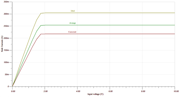
Advanced downstream-facing port (DFP) controller designs put low IQ as a key design goal. This type of design optimizes current consumption down to the microampere range. For example, the TPS25810 Type-C DFP controller draws less than 0.7µA (typical) when no device is attached. This helps AC/DC adapters comply with the required efficiency standards, and warrants long hold-up time for charged power banks.

With the low IQ design of advanced Type-C controllers, AC/DC charger designers can meet standby power requirements without having the extra burden of an additional control circuit. Power banks using low IQ controllers can extend their charge hold-up time effectively, creating a better user experience.

Additional resources:


Protect your BLDC motor drive with cycle-by-cycle current limit control – part 1

$
0
0

Brushless DC (BLDC) motors are popular because of their high efficiency, high torque-to-weight ratio, low maintenance and long life. A three-phase brushless DC motor consists of a three-phase wound stator and rotor with permanent magnets. The absence of brushes in a BLDC motor necessitates an electronic drive for proper commutation of current in motor winding.

The most common power-electronic drive for a BLDC motor is a three-phase H-bridge inverter. Motor-winding current is commutated based on the position-sensor feedback or sensorless algorithms. The BLDC motor is driven by 120-degree trapezoidal control in which only two windings are conducting at a time. The winding current is controlled with unipolar switching (soft chopping) and there each switch of the three phase inverter conducts for 120-degree electrical period. Calculate the winding current of the BLDC motor at any instant, using the electrical model of the motor as given in Equation 1. 

where V is the applied voltage across the two conducting windings, R is the line-to-line motor-winding resistance, L is the line-to-line motor-winding inductance and E is the line-to-line back electromotive force (EMF).

Equation 1 shows that instantaneous winding current depends on the back EMF, motor resistance, inductance and applied voltage. The motor’s back EMF is proportional to its angular speed; thus at a stall condition (zero speed), the back EMF is zero. This means that when the motor is stalled, the steady-state current in the motor winding is limited by the motor resistance only. When the motor gets saturated at high (over) current, the inductance drops, and current rises even quicker than at the nominal current level.

Consider an example of a BLDC motor rated for 400W, a rated DC voltage of 220V and a rated RMS winding current of 3.6A. The motor has a winding resistance of approximately 6Ω. Therefore the stall current = V/R = 220V/6Ω = 36.67A. This means that if you do not have proper current-limit protection, the inverter stage must be rated for 36.67A.

If the motor-drive system is allowed to carry the stall current:

  • The inverter stage must be rated for carrying the stall current, which makes the inverter stage bulky and costly.
  • Allowing the motor winding to carry stall current for a long time makes the motor overheat. This may cause burning of the winding. Also, the permanent magnets may get demagnetized due to high temperature or high demagnetizing current.

If you design the motor-drive system for a nominal current rating, you will need proper winding over current protection to protect the inverter stage and the motor. To implement winding over current protection, the first step is to sense the winding current.

Ideally, you could measure the three-phase winding current by placing current sensors in series with all of the phases, or placing current sensors in all of the inverter legs. Alternatively, you could sense two phase currents and determine the third phase current by equating the algebraic sum of all the phase currents to zero.

During trapezoidal control of a BLDC motor, for each 60-degree electrical commutation period, only two inverter legs are active and delivering power to the motor; the third inverter leg is kept in a high-impedance state by switching both the high- and low-side switches off. At any time only two phases are on. This implies that you can measure the winding current by sensing the DC bus current. You could place a low-cost sense resistor at the DC bus return to sense the motor current, as shown in Figure 1.

For a unipolar two-quadrant drive, apply pulse-width modulation (PWM) only to the high-side switch of one active leg. The low-side switch of the other active leg will remain on for the entire 60-degree electrical commutation period.

Consider a commutation period in which phases A & B are active. When the top-side switch is on, the two-phase winding will be energized and the current path will be as shown in Figure 1(a). When the top- and bottom-side switches are on, the DC bus current is the same as the winding current. When top-side PWM is low, the top-side switch goes off and the winding current will freewheel through the diode of Q2, as shown in Figure 1(b). During this freewheeling period (where the top-side switch is off and the bottom-side switch is on), the winding current is not flowing through the DC bus; hence the DC bus current is zero. The current does not increase during freewheeling, but decreases. This indicates that the DC-link current measurement is sufficient for winding overcurrent protection. Figure 2 shows the motor-winding current and DC bus current in 120-degree trapezoidal control.

Figure 1: Current path when top and bottom switches are on (a); current path when top-side switch is off and the bottom-side switch is on (b)

Figure 2: Winding current and DC bus current in 120-degree trapezoidal control


From my explanations thus far, you can see that it’s possible to control the motor-winding current by sensing the DC bus current. You can implement peak current-limit control by sensing the DC bus current and designing your inverter for the nominal motor current rather than overdesigning for the stall current. For low-inductance BLDC motors (typically from a few micro-henries to a few tens of milli-henries), a high winding resistance-to-inductance ratio leads to a high rate of winding current rise. The current-limit protection must be fast (well below 1µs) and act in every PWM cycle to avoid any short current spikes.

In part 2,I will discuss on how to implement the cycle-by-cycle over current protection by sensing the DC bus current and using an ultra-low power microcontroller.

Additional resources:

Why do you need a 5.5Vin buck-boost in a car?

$
0
0


An automotive-qualified buck-boost converter that’s only rated to 5.5VIN? With a 12-V car battery, you can’t connect the buck-boost to the battery. So who needs such a buck-boost converter? It turns out that sometimes a car has more than one battery, and backup batteries often require a buck-boost converter to provide power for certain electronics. Usually these batteries reside in the infotainment portion of the electronics, especially in emergency call (eCall) systems.

With all of the new electronics being introduced into cars – sometimes through government regulations– everyone should step back and consider if each car subsystem is still functional without the main battery present to power everything. Some systems must be able to function without the car’s tried-and-true 12V lead-acid battery. These systems require their own power source, which is usually a backup battery of their own. Of course, as with any battery, the voltage varies based on everything from the state of charge to the ambient temperature. Varying voltages require power-management considerations.

Additionally, backup batteries need charging. Since the car battery is almost always functional, it is a good power source for this task. Usually, the 12V car battery voltage is stepped down to around 5V and this voltage is given to both the charger and the system operating from the backup battery. If the car battery fails, the subsystem seamlessly switches over to the backup battery and continues operating. A buck-boost converter supports the different voltages of different power sources: backup battery or 5V rail.

The blog post, When to use a (4-switch) buck-boost converter, explains that a four-switch buck-boost converter is a simple and efficient way to properly convert power from an input source that has a varying voltage to a regulated output voltage. The new TPS63020-Q1 is a 4A automotive buck-boost converter that operates from 5V rails as well as single-cell lithium batteries. The high current rating with all internal MOSFETs makes it a very integrated power supply for providing 5V system rails, as well as higher-voltage and higher-power Global System for Mobile Communications (GSM) rails in eCall applications.

In both a 5V system rail and GSM supply application, the output voltage is both higher and lower than the input voltage, depending on which power source is present and the battery’s state of charge.

Check back soon with Behind the Wheel for more details about how to use the TPS63020-Q1 buck-boost converter in an eCall system.


Additional resources:

Learn more about the importance of battery management in an ecall system in this blog post.

Learn more about power solutions for eCall applications in this solution guide.

Reversing the voice quality gap

$
0
0

A guest post from Scott Kurtz, president, DSP Soundware

Human evolution is a constant when compared to the ever increasing rate of evolution of technology. Our input methods (sight, hearing, smell, taste, and touch) are what they are. Until technology enables our brains to interface directly with our electronics, our interface to the world around us will be via our five senses.

In the television, radio, and digital media spaces, we have done plenty to improve voice and sound quality over the years. But in the area of telephony we have actually taken steps back, especially in the early days of Voice-over-IP and cellular. Beyond that, improving hands-free communication such as speakerphone and hands-free cellular has always been challenging when it comes to speech quality. “Environmental issues” such as background noise, acoustic echo, and reverberation reduce not only human intelligibility but also the accuracy of automatic speech recognition algorithms. When it comes right down to it, these degradations simply sour the human communication experience.

When we instruct our voice-controlled thermostats to change temperature, we want the temperature to be set correctly on the first try. Imagine this: You have just done a load of dark laundry and your spouse is fuming when she/he sees that her/his favorite clothes have been bleached. It turns out that your dryer’s screeching motor bearings caused your newfangled washing machine’s speech recognizer to interpret the screech as “bleach.” In a Seinfeld-esque way, you plead with your spouse “It was the screech; it was the screech” to no avail. Now you’re wishing that your washing machine had some noise reduction to help its speech recognizer.

But I digress. Back in 2005, I gave a presentation titled “Bridging the Voice Quality Gap” at the Texas Instrument’s DSP Champs conference. The premise of the presentation was that Voice-over-IP and cellular gave us worse voice quality than did the ubiquitous wireline telephony, hence the term “voice quality gap.” We had taken a step in the wrong direction. The point of the presentation was that, through digital signal processing, we could not only narrow the gap but also strive to reverse the gap in favor of the newer technologies. In the early days of VoIP and digital cellular, much of the focus was on compressing speech into limited bandwidth channels. That compression was one of the reasons the voice quality soured in the first place. Since that time, bandwidth is far less constrained and HD voice is finally being introduced as a result. But that still leaves us with the “environmental issues” of background noise, acoustic echo, and reverberation. These environmental issues can be quite challenging because the environment is different for each user. The environment is comprised of the hardware, speaker, microphone, enclosure, and acoustic environment surrounding the user.

So, nearly ten years after my 2005 presentation, I formed a new company – DSP Soundware – with the mission to develop voice and sound quality enhancement technology, algorithms, and software.

Cleaning up that signal!

Voice and sound degradations are shown pictorially in the diagram below. The diagram shows a number of people in a conference room. There is a speakerphone on the conference room table and a fan on the right wall depicting a noise source. The person standing at the whiteboard is talking. The blue path shows his speech travelling directly to the speakerphone. The red path shows the talker’s speech reflecting off of the left wall. (It reflects off all surfaces, but only one reflection is shown.) The green path shows the output of the speakerphone reflecting back into its microphone. And finally, the brown path shows the noise of the fan as it travels to the speakerphone. At the other end of the phone call (not shown) is somebody trying to understand what is being said in the presence of all the distortion.

At DSP Soundware, we have developed voice and sound quality enhancement algorithms to combat these degradations. Our algorithms include acoustic echo cancellation, noise reduction, dereverberation, acoustic beamforming, and active noise cancellation. Referring back to the same diagram (above), we show pictorially how our algorithms remove the distortion in an attempt to recreate the undistorted signal. As the signal passes down through the algorithms, you can see the color coded distortion circles get “filtered” out, leaving only the light blue circle, which represents the clean speech.

The TI DSP advantage

Once we had the algorithms, we needed to turn them into usable embedded software products, and software needs to run on processors. I have been working with TI DSPs since 1984 when TI’s first DSP, the TMS32010, was introduced. TI has consistently had the best silicon combined with the best tools not only for an algorithm developer like me but also for end product developers. Today, TI offers the most diverse set of DSPs, microprocessors, and microcontrollers out there. And TI has a strong network of designers and developers that support its products.

For me, the decision to develop our software for use on TI products was more than a technical decision but also a business decision. TI silicon is a top notch choice for engineers who develop voice and audio applications.

Today we use TI’s OMAP-L138/TMS320C6748 LCDK board to demonstrate our algorithms. The LCDK board has audio input and output, an obvious requirement for demonstrating voice quality enhancement. But it’s also so inexpensive (the LC stands for low-cost) that any customer can purchase one, load our demonstration, and listen for him or herself. Our first such demonstration shows off our noise reduction algorithm. The user can feed noisy audio into the LCDK; our software processes the signal and outputs the noise-reduced version. The user can vary the noise reduction algorithm’s control parameters through a simple interface and listen to the result.

For the foreseeable future, voice communication is here to stay. Voice quality can be enhanced through the use of digital signal processing. By combining our algorithms and TI processors, we provide the building blocks to equipment designers to improve voice quality in their end-products. To that end, I hope we can help you.

Amp up your cans: Is your op amp stable? (Part 2)

$
0
0

This post is co-authored by John Caldwell.

In the first post in our “Amp up your cans” blog series, my colleague John Caldwell and I used a nominal value of headphone impedance to calculate the output voltage and current requirements of headphone amplifiers. The impedance of most headphones is not purely resistive, however. Headphones are notorious for being a difficult load for amplifiers, necessitating proper compensation to avoid stability issues, such as ringing and oscillations.

Numerous compensation techniques exist to address this issue using external components, but wouldn’t it be nice if the op amp didn’t need these additional components? During the development of the OPA1622, a high-performance, low THD+N, bipolar-input audio operational amplifier (op amp), we took on this challenge. Our goal was to minimize, if not eliminate, the need for additional components to maintain stability.

Figures 1 and 2 show the impedance magnitude and phase of several popular headphones. The magnitude plot clearly reveals a resonant peak around 1MHz. This peak results from the cable capacitance and inductance. Beyond this point, the headphone load is dominantly capacitive, as is evident from the phase shift at these frequencies, illustrated in Figure 2. On extracting electrical models for the headphone impedance, the value of this capacitance can be almost 500pF! 

Figure 1: Impedance magnitude of several headphone models

Figure 2: Impedance phase of several headphone models

Op amps are not usually designed to drive a large capacitive load. The capacitance interacts with the open-loop output impedance, RO, of the amplifier to introduce a pole, fpO1, in the amplifier’s open-loop gain curve, as shown in Figure 3. This pole causes excessive phase shift in the feedback loop, severely degrading phase margin. The reduced phase margin results in increased ringing in the amplifier’s step response and could potentially cause the amplifier to oscillate. The effect is worse in a unity-gain configuration.

Figure 3: The effect of op amp open-loop output impedance, RO,on capacitive load drive

A common solution is to use an isolation resistor, RISO, between the amplifier and the headphone load (Figure 4), but this heavily degrades audio performance, along with other penalties like reduced output voltage range. John’s article, “Stabilizing difference amplifiers for headphone applications,” examines in further detail the negative effects of series isolation resistors in headphone amplifiers. 

Figure 4: Isolation resistor to improve capacitive load drive

With the OPA1622, we took a different approach. We developed an output stage with very low output impedance that pushes the second pole (created by the capacitive load)to a higher frequency. We added additional poles and zeros to the open-loop gain curve at frequencies fpA and fzA (shown in Figure 5), choosing the location of the pole-zero pairs and the pole-zero separation to:

  • Provide high gain bandwidth (GBW) in the audio frequency range, resulting in a large loop gain that suppresses harmonic distortion over the audio frequency range.
  • Roll off the open-loop response to cross unity-gain well below the output pole, fpO2, resulting in sufficient phase margin with a large capacitive load. See Figure 5.

Figure 5: OPA1622 open-loop response vs. general-purpose amplifier for large capacitive load

Figure 6(a) shows the measured gain and phase response of the OPA1622. The pole-zeros in the response enable the gain to roll off faster with only minor changes in the phase response, allowing adequate phase when gain crosses 0dB. The gain bandwidth in the audio band is around 32MHz, with a unity-gain frequency (UGF) of 8MHz. Figure 6(b) shows the open-loop output impedance of the OPA1622.

Figure 6: OPA1622 open-loop gain and phase (a) and output impedance (b)

We designed the OPA1622 to have a low output impedance of 5.5Ω over a wide frequency range. This allows it to drive capacitive loads over 800pF in a unity-gain configuration, requiring no external components for compensation. See Figure 7.

Figure 7: OPA1622 phase margin vs. capacitive load

We demoed the device at the 2016 Consumer Electronics Show (watch John’s video of the demo) in a circuit that did not include any series isolation resistors. The OPA1622 was stable regardless of the headphone the attendees chose and we received overwhelmingly positive feedback regarding the sound quality.  

In part three of this series, we’ll take a look at slew rate, output drive and how the OPA1622 achieves ultra-low distortion while driving headphone loads.

Additional resources

Power Tips: Determining capacitance in a high-voltage energy storage system

$
0
0

High-voltage capacitive energy storage often provides power to repetitive high-power pulse loads such as a camera flash or radio transmitter. Storage capacitors supply a brief, high-power burst of energy to the load, but are then allowed to slowly recharge over a much longer time period. Their benefits generally include a lower average input current, which eases the requirements on the input source and reduces the size of the converter’s power stage. But storage capacitors can be quite large, so it’s beneficial to accurately determine the capacitance necessary in order to minimize their size. Let’s take a look at how to determine the required amount of capacitance.

The load discharging the storage capacitors can be categorized into three types: constant power, constant current or resistive. Figure 1 shows an example of how each type discharges a stand-alone 3400µF capacitor charged to 32V with an initial load of 69W. The constant power load, equivalent to that of a switching regulator, increases its current draw as the capacitor voltage decreases, further accelerating the voltage decay. To make things worse, the switching regulator’s efficiency also has an impact on the discharge rate. Converters such as boosts generally have lower efficiency as their input voltage decreases, drawing even higher power. Constant power is the most severe of the three types, requiring the most capacitance.

Figure 1: A storage capacitor’s discharge rate is highly dependent on the load type

A constant current load provides a linear discharge slope. This makes predicting the capacitor’s “end” voltage relatively easy. The power drawn from the storage capacitor decreases as its voltage decreases and only certain types of loads have these characteristics. Examples of constant current loads include integrated circuits or applications such as a constant current LED driver, whose current is regulated by a linear regulator.

A resistive load has an exponentially decaying voltage and the longest holdup. A resistive load type is the least common of the three. Examples include an incandescent bulb, heating element or active load.

Once you know the load type, you can use Equations 1, 2 and 3 to determine the necessary storage capacitance for a given holdup time. Based on the curve in Figure 1, a constant-power load such as a 12V buck regulator could operate for about 21mS before falling out of regulation. Alternatively, a constant current load could support at least 16V for 25mS before requiring a recharge. If you require a regulator to supply a fixed output voltage, be sure to factor in its efficiency, as it will shorten the holdup time. Equations 1, 2 and 3 are:

where  is the final capacitor voltage after time, t;  is the initial capacitor voltage;  is the discharge time;  is the load current;  is the storage capacitance;  is the power; and  is the resistance.

Energy storage with a repetitive pulse load requires an understanding of the load type and its impact on the storage capacitor’s discharge rate. This allows you to select the proper capacitor bank size to achieve the necessary timing. High-voltage capacitive storage provides an effective method to supply a large, short-duration energy pulse.

Additional resources

Roundtable audio loudness and quality evaluations for smart amplifier solutions

$
0
0

Making transducers sound as natural as possible is quite a challenge for audio tuners. While subjective evaluations help designers fine-tune sound, they face several challenges, such as visual cues impacting both audio perception and quality.

Objective measurements help mitigate some of the challenges posed by subjective evaluation. Objective evaluations also help when making A/B comparisons. When conducting objective or subjective tests, audio tuners prefer high-quality audio recordings over highly compressed MP3/AAC files. Raw WAV files are the best.

To perform objective analyses, you need a good-quality microphone; an audio sound card to capture the microphone data to your PC; and software tools like MATLAB, Audacity and Room EQ Wizard (REW).

Figure 1 depicts an experimental setup using the TAS2555 audio amplifier, a TI SmartAmp.

Figure 1: Typical lab setup for audio measurements

These are some of the objective parameters that can help audio tuners judge the perception of audio loudness and quality.

Loudness
One of the main objectives of TI’s TAS2555 is to drive the speaker to its maximum limits while protecting it against electrical or mechanical failures. The peak and average sound pressure level (SPL) measurements help determine this objectively.

I use REW for an analysis like the one shown in Figure 2, which also uses the TAS2555 audio amplifier to analyze a popular rock song.

Figure 2: SPL measurements

Timbre
It is imperative that while your solution should sound as loud as possible, it should not be at the expense of audio quality/timbre.

Audio timbre/quality represents the characteristics of music reproduction, which allows the human ear to distinguish sounds that have the same pitch and loudness. Timbre is directly related to static parameters like harmonic content and dynamic parameters like vibrato and the attack-decay envelope. The Acoustical Society of America (ASA) definition of timbre describes it as an “attribute of auditory sensation which enables a listener to judge that two nonidentical sounds, similarly presented and having the same loudness and pitch, are dissimilar,” adding that “… timbre depends primarily upon the frequency spectrum, although it also depends upon the sound pressure and the temporal characteristics of the sound.”

Although timbre is highly subjective parameter, audio researchers have tried relating subjective experiences to physical phenomena (objective parameters). Table 1 illustrates this mapping.

Table 1: Mapping subjective experiences to objective parameters

The subjective analysis is objectively possible by studying the tracks (the input being the raw file/audio captured from the reference system vs. the output being speaker audio captured via mic) with these parameters:

  • Global energy. You can compute the global energy of signal x simply by taking the root average of the square of the amplitude, also called root-mean-square (RMS) (Equation 1). In case of an A/B comparison, where the aim is to match the two solutions, the difference between the global energy of the two solutions should be as close as possible to zero.

 (1)

  • Key strength. Key strength in a given musical score is extractable through cross-correlation against the distribution of energy along the various pitches. If the speaker maintains the tonality of the music well, then the key strength estimated in the input file should match that of the file recorded using the mic that captured the speaker output.
  • Audio brightness. The brightness parameter indicates the evolution of brightness throughout a piece of music. High values indicate moments in the music where most of the sound energy is on the high-frequency content, whereas low values indicate moments where most of the sound energy is on the low-frequency content.
  • Energy roll-off. One way to estimate the amount of high frequency in a signal is finding the corner frequency below which a certain fraction of the total energy is contained. The lower the value returned, the darker the content, or the smart amplifier has been able to preserve the low and mid frequencies well.
  • Audio roughness. The roughness indicates the amount of sensory dissonance at each successive moment throughout a piece of music. The sensory dissonance corresponds to a “beating” phenomenon, where several sounds are heard with nearly the same frequency but with just a few hertz difference. Higher roughness makes the sound feel harsher.
  • Audio flatness. Spectral flatness, also known as Wiener entropy, is a measure used to characterize an audio spectrum. Spectral flatness provides a way to quantify how noise-like a sound is, as opposed to being tone-like. The meaning of tonal in this context is in the sense of the amount of peaks or resonant structure in a power spectrum, as opposed to the flat spectrum of a white noise. You can calculate spectral flatness by dividing the geometric mean of the power spectrum by the arithmetic mean of the power spectrum (Equation 2).
(2)

I used the TAS2555 as my example because it can use PurePath™ Console software, which helps you tune the solution to meet your signature sound. PurePath™ Console software is an easy-to-use audio-development suite that helps you evaluate, configure and debug audio products during development. Access to PurePath™ Console software enables you to identify issues and ensure the best possible sound.

TAS2555 vs. coventional solution
Table 2 shows the average values of timbre parameters for measurement across 18 different tracks from various music genres (blues, rock, classical).

Table 2 - Comparison of objective parameters between TAS2555 and a popular phone

Tuning an audio solution to get the most natural sound possible is often hard and takes a lot of time. There are several tools out there to help with this process; however, it is important to make sure that you account for (and correct if needed) the elements of sound that I’ve covered in this post. If you have had similar problems in the past, please leave a comment below. How do you fine-tune your sound?

Additional resources

Download the “Audio Accessory Designs From Start to Finish” e-book.

VIDEO: Inside the inspiring office of our SVP of sales

$
0
0

On every wall and shelf of Bing Xie’s office, motivation exists in abundance. Whether it’s a poster of Jack Kilby, the inventor of the integrated circuit (IC), or calligraphy hand written by his father, or a tiger statue to symbolize assertiveness, Bing sees constant reminders to work hard and sell more as the senior vice president of worldwide sales and applications.

His workplace, and all it symbolizes, was recently featured in a New York Times article showcasing the unique and inspiring elements that make up different work spaces. We encourage you to read the story.

Bing also opened his door for a video tour of his office, giving a deeper explanation of some of the items that keep him motivated each and every day. You can watch the video below:


Generating bias current networks with arbitrary magnitudes - Part two

$
0
0

In the previous post in this series, an equation was derived to describe the ratio of the Nth RSET resistor in Figure 1 below. 

Figure 1: Current Sink Network

That equation, again, is as follows:

So, what can be said about Equation 1? First of all, for an MIN ratio of 1, the corresponding MRN ratio will also be 1, as would be expected. Second, for values of MIN greater than 1, notice that the two terms of the denominator of Equation 1 take on different signs. This means that depending on certain physical quantities involved (Kn, RSET1, VREF), MRN can become arbitrarily large. Thus, this region should be avoided, instead favoring the MIN≤ 1 region; that is, by ensuring that ISINKN is less than or equal to ISINK1 for all N.

Notice that allowing the denominator of the root term in Equation 1 (the Kn, RSET1, VREF product) to become large results in a 1:1 linear relationship between MRN and MIN in the limit. Ultimately, the range of usable values that VREF and RSET1 can take on to increase this product are going to be limited by the headroom required for the sink; though it is worth noting that for a fixed ISINK1 value, increasing VREF requires an increase in RSET1 as well. The final variable in the product, Kn, is the process transconductance of the MOSFET and can be maximized through device selection. The effect of Kn on the linearity of the MRN, MIN relationship (across five decades of Kn values) is illustrated in Figure 2 below.

Figure 2: Resistor Ratio vs. Current Ratio Across Process Transconductance

The process transconductance is so named due to its dependence on carrier mobility, oxide permittivity, and oxide thickness (μ, εox, tox)—all material and process properties:

However, it is also dependent on the W/L ratio of the device, so in general larger devices will result in increasingly linear behavior in Equation 1. While most datasheets will not include Kn, it can be calculated from a common datasheet parameter, the forward transconductance, often listed as gm or gFS:  

Recall that the drain current equation for an NMOS operating in the saturation region is:

Neglecting channel length modulation and rewriting the terms of Equation 4:

This result can be substituted into Equation 3 and ultimately solved for Kn

Thus, using Equation 7 it is possible to select optimal MOSFET devices for the bias network. Further, having obtained this value, it can be utilized in Equation 1 to calculate (more accurately) required RSETN resistor values to produce desired ISINKN currents.

It is important to note that Equation 1 tends to overestimate the RSETN resistance in the MIN≤ 1 region; that is, it results in currents that are lower than the desired value. However, the ideal transistor case (MIN=MRN) will always underestimate the RSETN resistance in this region. Thus, calculating these two values will ultimately bound the exact value required.  Consider two randomly chosen NFETs, 2N6755 and IRFZ40, which have listed gFS values of 5.5A/V2 (at ID=9A) and 15A/V2 (at ID=31A), respectively. Suppose these are used to implement an MIN ratio of ¼; the corrected RSETN and MRN ratios are calculated using Equation 1 (along with some straightforward design values) in Table 1 below.

Table 1:  Circuit Parameters and Calculated RSETN and MRN for MIN

Using the conditions listed above for the IRFZ40 transistor, Figure 3 displays the results of a TINA-TI simulation of the circuit in Figure 1 implemented with RSETN values calculated from the ideal case (5Ω under these conditions), the corrected case (Equation 1), and the average of these two. 

Figure 3: Sink Current vs. Drain Voltage for Ideal, Corrected, and Average RSETN Values

The results for simulations using both the 2N6755 and IRFZ40 with the three RSETN values (as described above) are summarized along with corresponding percent error calculations in Table 2 below.

Table 2: RSETN Calculation Methods and Resulting Accuracy 

Ultimately a single feedback device can be used to derive a bias network of arbitrary values so long as certain conditions are met: particularly that the current in the primary feedback driven leg is the largest in the network, and the proper headroom is maintained in each leg. Thus, from a single voltage reference, a bias network is established.

MSP432™ microcontrollers are on fire

$
0
0

Things are heating up with MSP432 microcontrollers, so much so that it was included in EDN’s Hot 100 2015 list. The list highlights the electronic industry’s most significant products of the year based on innovation, significance, usefulness and popularity.

 In case you need a quick refresher, the MSP432 microcontroller is the highest performing MSP MCU that leverages MSP’s 16-bit and 32-bit ARM® Cortex®-M4F portfolio. It features best in class analog performance with 24-ch 14-bit (13.2 ENOB) differential ADC up to 1 MSPS. The fun doesn’t stop there; the platform has incorporated the best-in-class MSP430™ microcontroller hardware, software and cloud tools to offer seamless integration for current MSP430 microcontroller developers. The device can operate at a full speed down to a supply of 1.62V, simplifying direct sensor interface. It specs an operating current of 95 µA/MHz and a sleep mode current of 850 nA with its real-time clock running. Check out our blog here to learn more about why the MSP432 microcontroller is so hot. 

The great news doesn’t end there; we also recently announced that the MSP432 microcontroller is now fully CMSIS compliant. We heard ARM developers rejoice when we shared this news! Developers are now able to quickly develop more portable, re-usable and compiler-independent code. To learn more, read our blog here.

In need of more MSP432 microcontroller resources? Visit the links below.

Get connected with WEPTECH's 6LoWPAN IoT gateway solution

$
0
0

Guest blog post by Sarah Nett, Weptech, www.weptech.de/contact.html 

What is the problem you are solving and how?

WEPTECHs 6LoWPAN Internet of Things (IoT) gateway provides an affordable, open-source-based solution for connecting 802.1.5.4 based 6LoWPAN-based IoT networks to the Internet.

The use of NAT64 allows addressing IPv4 servers from any 6LoWPAN node. NAT64 is an established interim mechanism, which converts IPv6 to IPv4. Therefore, e.g. sensor data from the radio network can be transmitted to servers located anywhere in the Internet. A native IPv6 operation (“Bridge Mode”) is also possible.

What is unique and differentiated about your gateway solution?

By providing both 2.4 GHz and Sub-1 GHz radios, together with Ethernet and an ARM® Cortex®-M3 microcontroller (MCU), the gateway is able to work as a dual-band receiver and can handle both frequencies on the same board. It just takes a few easy steps to prepare the gateway.

When acquiring the WEPTECH gateway, developers can easily experience a neat solution for bridging 6LoWPAN wireless networks via an Ethernet connecting with TI’s SimpleLink™ multi-standard CC2650 SensorTag kit. Developers simply need to download the WEPETCH manual and follow the documentation.

The gateway offers out-of-the-box support for the Contiki border router firmware, which allows an immediate start and makes it integral to integrate the CC2650 SensorTag kits with existing IP networks. Compared to other options, this gateway is focusing on ease of use by not having a management interface for configuration and instead it simply gets an IPv4 address via DHCP. Just connect to the network and provide power.

You can find directions to connect the SensorTag kits with the gateway here.

What is the hardware and software offering?

The gateway is based on the ARM® Cortex®-M3-powered 6LoWPAN CC2538 wireless MCU that provides an AES and SHA encryption engine and embeds 512 kB of Flash memory and 32 kB of RAM. The board provides dual-band operation with two radio interfaces: the CC2538 wireless MCU integrates an 802.15.4-compliant radio interface in the 2.4 GHz band and an extra Sub-1 GHz transceiver (TI’s CC1200 RF transceiver) enabling use in the 868 or 915 MHz frequency bands.

The connection to the Internet is enabled via a 10BASE-T Ethernet interface, implemented using an Ethernet Controller.  

The software is based on the open source Contiki OS with the source code available for download via Github (http://www.contiki-os.org/).

After acquiring the WEPTECH gateway kit, WEPTECH offers hardware and software consultancy.

What markets is the gateway targeted for?

The audience includes every developer who wants to create solutions in the direction of 6LoWPAN on the basis of 802.15.4. Especially in the areas sensor networks, smart homes and street lighting, the Weptech IoT Gateway provides a neat solution for bridging 6LoWPAN wireless networks and Ethernet. A connection to a smartphone or tablet is also provided.

Which are the product key features highlight and benefits?

  • Powerful microcontroller with AES and SHA Encryption Engine with 512kB Flash, 32kB RAM
  • Dual-band operation: 2.4 GHz or 868 / 915MHz
  • Tabletop / wall-mount enclosure
  • Internal antennas (U.FL optional)
  • 10BASE-T Ethernet
  • Serial interface and firmware-update via USB
  • An established interim mechanism “Plug-and-Play“ NAT64
  • A native IPv6 (“Bridge Mode“), allowing network integration
  • Source code available for download
  • Power supply via USB microcontroller

Get started developing today with the WEPTECH 6LoWPAN IoT Gateway which is supported on and by the platform Contiki.  Additionally, buy your very own SensorTag kit to connect your gateway to sensors and more. 

A flexible, easy-to-design MicroSiP power module for portable test and measurement

$
0
0


Test and measurement equipment such as oscilloscopes and waveform generators has its own set of design challenges, from increasing measurement accuracy to providing a low-cost solution to the customer. Measurement accuracy, bandwidth and throughput (or channel count) are critically important to engineers using test equipment, but cost is key as well; after all, managers often must justify equipment purchases by showing that there will be a significant return on investment.

While portable test and measurement equipment is absolutely required for debugging some circuits, adding portability to the feature mix does not help the performance vs. cost trade-off. How should test-equipment manufacturers tackle the design of portable test equipment with these trade-offs in mind?

One way is to simplify and shrink the power-supply portion of the test-equipment system. Numerous power-supply circuits are required to power so much functionality and so many subsystems. If you could use one circuit for most or all rails, the design effort and design cost for the entire power supply would be greatly reduced through the design reuse of that one circuit. This allows faster time to market and less design resources spent on the power supply.

What if this one circuit, in addition to being flexible, was simple to design, very small and efficient, and had low noise? That would enable the test equipment to become portable in short order – keeping efficiency high and noise low while reducing board space occupied and design effort required.

A new MicroSiP power module, the TPS82084, addresses all of these wants and needs. Packaged in a tiny 2.8mm-by-3mm package and occupying 35mm2 total, it requires only two capacitors and two resistors to complete the entire power-supply solution. It includes the power inductor, eliminating the sometimes time-consuming task of selecting one yourself. The two resistors allow you to set the output voltage anywhere below the input voltage – so you can use this one device for all of the system voltage-rails. This saves your R&D budget by reducing the power-supply design effort required.

Figure 1 shows the device, which even has quad flat pack no-lead (QFN)-style mounting for ease of assembly onto the printed circuit board (PCB). A thermal pad allows a low thermal resistance, enabling operation up to its full rated 2A current even above a 100°C ambient temperature without airflow.

Figure 1: The TPS82084 MicroSiP power module features QFN-like pads for easier assembly onto the PCB

The 17µA quiescent current (IQ) provides high efficiency at light loads, while its DCS-Control topology enables a very low noise power-save mode in order to power subsystems without interference. Figure 2 shows above 90% efficiency at heavier loads. Finally, if firmware upgrades or feature creeps require more than 2A, the TPS82085 provides a pin-to-pin upgrade to 3A.


Figure 2: The TPS82084 provides over 90% efficiency

How can a MicroSiP module enable faster designs in less board space for your test equipment?

Additional resources


TI Accelerated the Driving Experience at CES 2016

$
0
0

It’s hard to believe that yet another CES has come and gone, and 2016 was the best year yet. With 32 automotive demos, featuring TI technologies ranging from ADAS and Infotainment to Audio, Haptics and DLP Products, TI demonstrated how its automotive technology is accelerating the driving experience.

If you couldn’t make it to Las Vegas for the show, don’t fret. Belowis a list of automotive demos showcased.  Below you will find a list of all the automotive demos with descriptions as well as links to videos of the demos:

  • The Evolution Car (EvoCar) demo
  • This demo is a working showcase of TI’s automotive portfolio, featuring DLP® Products, advanced driver assistance systems (ADAS), infotainment, haptics and LED Matrix Headlight Manager.
  • ADAS
  • DLP

  • 3D perception with structure from motion (SfM) on TDA2 processors for semi-autonomous driving
  • 3D perception and mapping of the surrounding using SfM for parking assist/semi-autonomous driving leveraging the real-time performance of the TDA SoC family. The EVE architecture provides >8x performance efficiency over ARM® only architectures.
  • Featured devices: TDA2, DS90UB913A–Q1, DS90UB914A–Q1, TPS659039–Q1, LM53603–Q1, DS90UB925–Q1, HVDA55x–Q1

  • 3D surround view on TDA2 processors with joystick control
  • Real-time 3D surround view (SV) with full user control of virtual camera with TDA2 & TDA2Eco SoCs. The architecture supports 3D SV with other ADAS applications with DSP and EVE cores, as well as efficient photometric processing on the C66x DSP.
  • Featured devices: TDA2, DS90UB913A–Q1, DS90UB914A–Q1, TPS659039, LM53603–Q1, DS90UB925–Q1, HVDA55x–Q1

  • Low-cost smart 3D surround view on TDA3 processors
  • Ultra-low cost system BOM with TDA3 SoC-based solution. Hardware accelerated 3D surround view visualization (no GPU) for a low power solution with ISP feature integration. The demo showcases TI-D3 Ruggedized Vision Platform for rapid prototyping.
  • Featured devices: TDA3, DS90UB913A–Q1, TI CSI2 HUB, TI PMIC, DS90UH925–Q1, TPS22965–Q1, LM53603–Q1, HVDA55x

  • EuroNCAP 2018 front camera on TDAx processors
  • Scalable EuroNCAP 2018 solution on TDA2 SoCs for high-end and TDA3 SoCs for mid- to entry-level vehicles. Applications include pedestrian, lane, vehicle, bicycle detection, traffic sign/ light recognition and high beam assist.
  • Featured devices: TDA2, TPS659039–Q1, LM53602–Q1, HVDA55x–Q1, TDA3, TI PMIC, TPS54340–Q1

  • TDA2 processor-based xCAM platform
  • Front camera algorithms on the TDA2 based xCAM platform deliver pedestrian, lane, vehicle, bicycle detection, traffic sign/ light recognition and high beam assist. The platform is enabled by EVE architecture providing >8x performance efficiency over ARM® only architecture.
  • Featured devices: TDA2, TPS659039–Q1, LM53602–Q1, HVDA55x–Q1

  • Low-cost driver monitoring on TDA3 processors
  • Driver monitoring (DM) solution with face detect/recognition, side and down alert and eye closure. This demo showcases a scalable solution with TDA3 processors supporting low-cost to high-performance sing to multi-camera DM systems.
  • Featured devices: TDA3, TI PMIC, TPS54340–Q1, HVDA55x–Q1

  • Camera monitoring systems (CMS) with TDA3 processors
  • Driver monitoring (DM) solution with face detect/recognition, side and down alert and eye closure. This demo showcases a scalable solution with TDA3 processors supporting low-cost to high-performance single to multi-camera DM systems.
  • Featured devices: TDA3, TI PMIC, TPS54340–Q1, HVDA55x–Q1, TI CSI2 FPD-Link HUB

  • “Jacinto 6” processor integrated automotive Linux™
  • Integrated automotive-grade Linux-based infotainment solution showcasing music / video players, rear-view camera, AM/FM radio, 3D navigation graphics display and Android smartphone interface as well as a CAN-controlled warning display.
  • Featured devices: DRA7xx, TPS65xx, WiLink™ 8Q

  • “Jacinto 6” family ready for secure and trusted V2X applications
  • Demonstrates ECDSA performance for “Jacinto 6” architecture: supports worst-case message rates up to 200/sec for verify on-demand and up to 400/sec for verify all. ARM® Cortex®-A15 supports both the communications and applications stacks and TI C66x DSP and ARM968 cores cover the message authentication processing required for V2X system with Elliptic Curve Cryptography.
  • Featured devices: DRA72x

  • Automotive audio: TAS6424-Q1: automotive load diagnostics
  • Load diagnostics is a method to detect if a load is open or shorted; it also detects if the output is shorted to ground or battery. It is needed during the assembly of the vehicle; the factory is loud, so audible listening is difficult, especially in systems with many speakers. This solution enhances system reliability with continuous diagnostics and protection.
  • Featured device: TAS6424-Q1

  • Aito touch automotive demo
  • This demo features Piezoelectric Touch Sensing with haptic feedback for button/switch replacement and the form factor is specifically for automotive. It is immune to moisture, works with gloves and has a smooth, sleek design. It is also thin and easy to manufacture.
  • Featured devices: DRV2700, MSP430

  • TI power solution driving automotive EPS, ADAS surround view, and infotainment
  • Miniature car demo showing electronic power steering (EPS), ADAS surround view, infotainment and cluster systems utilizing TI integrated power devices designed to support functional safety systems.
  • Featured devices: TPS65917-Q1, TPS65381-Q1, DRV3201-Q1

  • LED active matrix headlamp: dynamically controlled high/low beam system
  • This demo controls up to 96 LEDs from a single serial port for headlamp beam forming and directional control. It features an individual 10-bit PWM brightness control LED for pixel level light intensity adjustment. The LED open/short fault diagnostics and reporting alerts the driver in the event of headlamp failures or damage. It has feed-through architecture for easier routing on metal core PCB.
  • Featured devices: TPS92661, LM5122, C2000

  • USB Type-C solutions
  • TI offers the widest product selections for the emerging USB Type-C technology. TUSB32x enables Type-C configuration with flexible control interface. HD3SS460 enables Display Port Alternate mode over USB Type-C, HD3SS3212 and HD3SS3220 enable the lowest power Type-C connections.
  • Featured devices: TUSB2xx, HD3SS460, TUSB32x, HD3SS3212, HD3SS3220

  • Automotive phone infusion demo
  • As the world’s first bi-directional redriver, TUSB211 enables Apple CarPlay and charges the phone simultaneously through USB interface. TUSB211 has the world’s smallest QFN with flow-through packaging, allowing efficient signal routing while achieving 70% power reduction when comparing tofull packet repeater.
  • Featured device: TUSB211

  • HDMI2.0 6G signal conditioners
  • With the state of the art CDR technology for best signal quality and the lowest power consumption, TI’s HDMI2.0 signal conditioners are the best choice to enable 4K ultra sharp images.
  • Featured devices: TMDS181, SN65DP159

  • Automotive wide VIN buck converters for low EMI
  • This demo illustrates how 2 MHz switching and spread spectrum can dramatically reduce EMI in automotive applications. It uses the LM53601 2MHz, 36VIN, 1A Step-Down Converter to illustrate how spread spectrum reduces harmonics.
  • Featured device: LM53601

  • Automotive cluster tell-tale driver demo with TLC6C5712-Q1 LED driver
  • Twelve TLC6C5712-Q1 devices, controlled via a tablet, are used to drive almost 500 LEDs. Each LED can dim 256 steps current independently with diagnostics read back. It can also be used in bar graph, sequential turn indicator, & RGB light bar.
  • Featured devices: TLC6C5712-Q1, CC3200

  • BQ76PL455A-Q1 16-channel monitor/protector with passive balancing
  • Stackable monitor and protector for use in large format Lithium-ion batteries that provides monitoring, passive balancing, and communications. Helps systems to provide accurate state of charge and state of health calculation. Up to 16 bq76PL455A-Q1 EVM modules can be stacked.
  • Featured devices: bq76PL455A-Q1

  • EM1402 16-channel monitor/protector with 5A active balancing
  • Stackable monitor and protector for use in high-performance large format Lithium-ion batteries that provides monitoring, 5A active balancing, and communications. Up to 16 EM1402 EVM modules can be stacked. Demonstration shows balancing of 16 Lithium-ion cells via external 12V supply/battery.
  • Featured devices: bq76PL455A-Q1, EMB1428Q, EMB1499Q, LM5018M, ISO7342FCDW, LM5110-3M, LP2951-50DRGR, CSD17555Q5A, CSD18504Q5A

  • Automotive short-to-battery protection USB hub/head unit
  • Showcase of the TPD3S714-Q1 TI Design helps designers evaluate the operation and performance of TI’s first series of short-to-battery protection solutions. The TPD3S714-Q1 provides best-in-class bandwidth, leading over-current protection and the most reliable short-to-battery Isolation.
  • Featured devices: TPD3S714-Q1, TUSB4020BI-Q1, LMR14030

  • Aftermarket head-up-display (HUD) demo
  • Aftermarket HUD demo featuring DLP® Pico™ technology.
  • Featured devices: .24” VGA DMD, DPP2607 Controller, PAD1000, DLPC2607ZVB, LM75AIMMX/NOPB, MAX3221EIPWR, OPA2348AIDGKR, PAD1000YFFR, LM339PWR, TPS2051CDBVR, TPS62175DQCR, SN74AUP1T08DCKR, SN74AUP1G125DCKR, BQ24040DSQR

  • Resolver sensor interface demo
  • PGA411-Q1 is a resolver to digital converter with the excitation amplifier and boost supply integrated. This enables functional safety, overall BOM cost and PCB area reductions. The device has a number of features that are programmable. This helps customers with system customization, flexibility in sensor, and overall platform scalability.
  • Featured devices: PGA411-Q1, C2000, DDRV8848


Learn the inner workings of a CAN bus driver and how to debug your system

$
0
0
Welcome to the third post in this series about the controller area network (CAN). In my last post, I focused on what CAN bus signals look like in terms of voltage levels on the bus pins. In this post, I’ll focus on the typical topology of the CAN...(read more)

How batteries may make travel on Mars easier

$
0
0

I recently went to see the movie “The Martian.” Being the engineer that I am and working for such a large engineering company, the story of Mark Watney's perilous journey above the deserted planet, really resonated with me and possibly with engineers alike. As I watched, the main character, Mark Watney, encounter one problem after another, I found myself wondering how I could have helped or if I would have done things differently. With one of Watney’s biggest problems related to his transportation across Mars, I knew I could help there.

Throughout the movie, Watney travels to various locations to find equipment from previous missions that would help him communicate better with NASA, as well as equipment that he would ultimately use to complete his most perilous journey yet: a 3,200km journey to the Ares 4 habitat. He rigs up a Mars rover using two rover batteries and 14 solar panels for charging.

Looking into the engineering Mark puts into the battery pack I started to wonder what TI could offer to aid Watney. As a product marketing engineer of the Battery Management Solutions (BMS) organization, I know the devices we build for electric vehicles (EVs) typically have battery packs with 90kWh capacities ranging in configurations of 96 series cells by 77 parallel cells. According to the novel, The Martian, the battery Watney uses is a mere 9kWh for one battery, and he only had two of them.

With TI’s battery management devices you are able to accurately measure each battery cell (voltage, current and temperature measurements) in large-scale battery packs. Such devices include the bq76PL455A-Q1 (16-channel battery monitor) and the bq76PL536A-Q1 (3S- to 6S-channel battery monitor). Both devices measure a smaller group of cells and have a certain degree of stackability to allow flexibility in scaling. By using an accurate, scalable monitor, you can increase your runtime by being power-efficient, and always know the full capacity of your battery pack.

With an electronic vehicle (EV) type battery system, the Mars rover would provide about four to five times the runtime to travel a couple of hundred kilometers, despite the heavier battery. A longer runtime would have reduced the number of times Watney had to stop during his journeys to recharge the rover’s batteries.

Active cell balancing is another technology that could benefit a Martian EV to manage the batteries properly. Temperature can have the largest impact on a cell’s performance by causing changes in the cell’s impedance. If an equal load is applied to all cells but some cells are at different temperatures, the cell materials will be subject to additional expansion and contraction. This all leads to very different aging characteristics. The result is a charge mismatch – and because the cells will age differently, soon there will be a capacity mismatch (Figure 1). If left unmanaged, the overall pack capacity becomes limited by the lowest cell voltage, leading to a reduced vehicle range.

Charge mismatch                                                                    


Capacity mismatch


Figure 1: Charge mismatch vs. capacity mismatch


There are two basic types of cell balancing: passive balancing and active balancing. Here is a brief list of the basic features and benefits of each:


Passive balancing:

  • Simple to implement (hardware and software).
  • Cost efficient.
  • Reduces charge mismatch.
  • Small balancing current (<1A).

Active balancing (Figure 2):

  • Energy-efficient.
  • Reduces the effect of charge and capacity mismatch.
  • Works in charge and discharge.
  • Large balancing current (>1A).
  • Can quickly balance large batteries.
  •  Increased usable capacity.
  • Faster pack charge time.
  • Higher heavy charge/discharge duty cycle-capable.
  • Longer pack lifetime.
  • Mix/match new/old modules.
  • Can use mismatched cells within modules (increase production yield).


Figure 2: TI Designs (TIDU239) EM1401EVM simplified architecture


When choosing battery management solutions, active balancing would allow the most usable capacity from the batteries. All of the cells would be kept within millivolts of each other at all times, and Watney would always receive the most from the pack. The rover batteries, managed by TI’s EM1401EVM boards using the EMB1428Q and EMB1499Q active cell-balancing devices from TI, would provide high-performance 5A active cell balancing to get the most usable capacity from the batteries – for any journey across any planet.

Additional resources:


.


Easy supercap backup power for smart grid

$
0
0


Figure 1: Backup power lasts for 6.5 seconds

Everyone wants reliable smart meters. Utility customers want them so that the utility knows exactly when there is a power outage without the customer having to tell them. Early notification allows the utility to move quickly to restore power. The utility wants them so that they don’t miss even a portion of customer usage. After all, they can’t charge you for consumption if they don’t know for sure what you consumed.

One aspect of reliability is ensuring that the smart meter electronics always have enough power to perform the required tasks. A backup power source is usually required to properly handle the inevitable power losses that all meters face. During the short backup time, the meter records utility customer usage and sends a warning back to the utility. For meters powered from just a lithium primary battery, the backup power source may also serve the role of buffering the battery to provide peak power for data transmission. A single super capacitor (super cap) performs this role, as shown in the TI Designs Energy Buffering for Long-Life Battery Applications Reference Design.

Two super caps store twice the energy of one. Furthermore, two super caps connected in series support twice the voltage of one. Systems needing longer backup times or higher power during backup require a higher storage voltage or more energy storage. Connecting two super caps in series, however, presents a couple of challenges: how to balance the voltage on each super cap and how to charge them to the higher voltage in order to store more energy.

When connecting super caps in series, the voltage on each capacitor must remain within its rating. For example, if two 3V-rated capacitors are connected in series and charged to 6V total, slight differences in capacitance, equivalent series resistance ESR, leakages and so on can unbalance the capacitors such that one carries 4V while the other has only 2V. Clearly, this is not a reliable situation, since the 4V exceeds the capacitor’s 3V rating. While you could use passive resistors to overcome small differences in leakage currents that could lead to imbalance over time, you must use an active device instead to keep the voltages balanced during the high-current charging cycle.

The TI Designs Supercapacitor Backup Power Supply with Active Cell Balancing Reference Design does just this. Figure 1 shows the simple design, which charges and discharges two super caps while balancing them. For more details, see the test report.

Figure 2: Simplified block diagram of the backup power system

This design also charges the super caps to a higher voltage than the main input-power source. Assuming a 3.3V or 5V input power source, the TPS63020 buck-boost converter boosts the voltage up to 5.5V on the super caps. When backup power is needed, it efficiently regulates the varying super-cap voltage to the system for the backup time. Figure 1 shows that, with two stacked 3F super caps, the buck-boost converter provides 1.5W to the system for 6.5s.

Just want to use a single super cap? Here’s a simple way to get nearly all the power out of that super cap and drain it all the way.

What backup power scheme do you have in your smart meter

Pump it up with charge pumps – Part 1

$
0
0

Life was simple when I first became interested in electronics. Components were so big I could solder them without a microscope. Switching converters switched at a whopping 25 kHz, digital circuits all used a 5-V supply voltage and all the computers I came across used the RS-232 serial interface to communicate.

The RS-232 standard specifies that a logic 0 is represented by voltages between 5 V and 25 V, and a logic 1 by voltages between –5 V and –25 V. My problem was that although almost all the components on my boards needed only a 5-V supply, I still had to generate those two extra rails for my RS-232 interface.

Then I came across the MAX232. This device was an inspired product, combining two line drivers, two line receivers, and a positive and negative charge pump. With that bad boy running off a single 5-V supply, I could generate the additional supply voltages I needed and transmit and receive serial data.

Charge pumps are useful little DC/DC converters that use a capacitor to store energy instead of an inductor. They can be found in dedicated charge-pump devices such as the LM2775/LM2776 devices, as auxiliary rails in LCD bias supplies such as the TPS65150, or as external circuits put together from a couple of diodes and a couple of capacitors.

Generally speaking, charge pumps are:

  • Simple, often comprising no more than two diodes and two capacitors.
  • More forgiving than DC/DC converters.
  • Good for output currents in the tens of milliamps range (but not so good for currents much higher than 250 mA).
  • Less efficient than inductor-based DC/DC converters, unless they are unregulated and running open -loop.

Figure 1 is a simplified circuit diagram of an unregulated charge pump. The charge pump operates in two phases:

  • During the charge phase, switches S1 and S4 are open and switches S2 and S3 are closed. Current flows through S2 and S3 and charges the flying capacitor, CFLY, up to a voltage of VI.
  • During the discharge phase, switches S1 and S4 are closed and switches S2 and S3 are open. The negative terminal of CFLY is now at VI and the positive terminal (which is VI volts higher) is now at 2VI. Current flows from VI through the flying capacitor CFLY and switches S1 and S4. Charge is transferred from CFLY to the output capacitor, CO, to generate an output voltage approximately equal to 2VI.


Figure 1: Simplified charge-pump block diagram (voltage doubler)

You can rearrange the same four components (S1, S2, S3 and S4) to generate a negative output voltage equal to approximately –VI (see Figure 2).


Figure 2: Simplified charge-pump block diagram (voltage inverter)

The circuit just described works well, but its output voltage is unregulated. Such a simple circuit is sufficient is some applications, but a charge pump with a regulated output is much more useful.

The usual way to regulate the output voltage of a charge pump is to put an adjustable current source, I1, in series with switch S1, or S2 in the case of an inverting charge pump (see Figure 3). The error amplifier, A1, adjusts the value of I1 until the output voltage is correct. Under steady-state conditions, I1 is exactly twice the value of IO.


Figure 3: Different charge-pump integration levels

Note that a simple, regulated voltage doubler can only regulate its output voltage in the range of VI to 2VI. It cannot generate output voltages lower than VI. There are some fancy tricks you can do to make a buck-boost charge pump, but these kinds of devices are more complicated than the one shown in Figure 3.

Additional resources:

How to quickly prototype your pico display application by selecting the right optical module

$
0
0
Texas Instruments DLP ® Pico™ technology can enable a broad number of applications, ranging from head-mounted displays (HMD) to mobile smart TVs. As many hardware developers with limited knowledge in optics would like to quickly and easily integrate...(read more)

Enter your project to the Europe TIIC 2016 to win $5,000!

DIY your game watching party

$
0
0

Looking to throw an awesome party for the big game? DIY parties aren’t just for baby showers and wedding receptions. Here are three DIY hacks to take next Sunday to the tech level:

Cheer 'em on– Bring some team spirit to the party with the FanFlare wearable light display. The louder you yell, the faster your FanFlare blinks. Do you root for more than one team? Not a problem! The device has a slot where you can change out the graphic printed on transparency film. Created by TIer and DIYer Jason Rubadue, get FanFlares for all your game geeks here.TI Avatar
Forget the grill– Let your chicken wings cook themselves with this DIY with TI Wi-Fi-controlled sous-vide system. Being a DIYer and a foodie, TIer Trey German combined his passions with a common crockpot and several TI devices to make the perfect wings without the hassle. Using a MSP430F5529 USB LaunchPad™ Development KitSimpleLink™ Wi-Fi® CC3100 BoosterPack™ plug-in moduleADS1118 thermocouple BoosterPack and custom TRIAC board, Trey drops in the chicken wings, sets the crockpot to 170 degrees and checks back in four hours for the perfect game time grub.TI Avatar

Brew your own– Ensure your fans always have a cold one with this DIY homebrew kit. TIer and DIYer Leo Estevez uses an MSP430G2553 microcontroller (MCU), our NexFETs, Bluetooth® and power management components to create an in-house microbrewery. If you’re ready to start brewing, download Leo’s free, open source phone app here. And don’t forget the open source hardware and schematics here.TI Avatar

For other DIY projects, check out our DIY with TI blog series. Can’t get enough DIY with TI? Our annual DIY with TI event will take place on a number of our campuses across the globe on April 18. Follow along on our social channels and Think. Innovate to learn about the latest projects.

Viewing all 4543 articles
Browse latest View live


<script src="https://jsc.adskeeper.com/r/s/rssing.com.1596347.js" async> </script>