Quantcast
Channel: TI E2E support forums
Viewing all 4543 articles
Browse latest View live

Bringing Bluetooth® low energy to Sub-1 GHz networks with SimpleLink™ CC1350 wireless MCU

$
0
0

In today’s Internet of Things (IoT) world, there is a multitude of new wireless connectivity applications entering the market each day, propelling the continuous gathering of sensors and interactions.  From our smartphone reminding us it is time to leave for an event so that we will be on time, to our security system notifying us that no door is left open, we have a safety net of reminders helping us move throughout our day.  These IoT devices typically have several hard-to-meet requirements.  They need to operate on either Sub-1 GHz or 2.4 GHz RF bands to synchronize with already implemented systems.  To encourage seamless, non-invasive sensing, you need a tiny form factor that can go unnoticed in your everyday life.  This allows for the magical side of the IoT, where things around you just happen such as your home air conditioning kicks on when you are 20 minutes away, or your refrigerator adds milk to your shopping list because your daughter finished it with her afternoon snack.  To accomplish this you need ultra-low power consumption and high integration, all in a tiny form factor.  TI’s answer is the SimpleLink™ dual-band CC1350 wireless microcontroller (MCU), which is small enough to fit on your fingertip. 

Save on size and power with the new CC1350 wireless MCU.  The CC1350 solution is the latest device in the SimpleLink wireless MCU family released in early 2015.  The CC1350 device is a highly integrated dual-band solution supporting Sub-1 GHz and Bluetooth® low energy on the same chip.   Like the other devices in the SimpleLink family, it is designed with the same ultra-low power requirements in mind, along with market leading low power MCU and radios.   The CC1350 wireless MCU also utilizes the sensor controller to handle analog and digital sensors in a low-power manner. It is designed to run autonomously when the rest of the system is in standby.  Perfect for saving power in a sensor node network where power is your main concern.  To learn more about enabling longer battery lifetimes read the “Taking Power to a new low with the SimpleLink ULP wireless MCU platform” blog post.


Figure 1: SimpleLink dual-band CC1350 wireless MCU power numbers

We have covered size and power, so what does dual-band bring to the table? How would you utilize Sub-1 GHz + Bluetooth low energy? Let’s talk about some of the use cases. 

Let’s consider a house with a network of three smoke detectors.  Typically there are detectors placed in different rooms, such as your kitchen, entry hallway and near the bedroom.  The smoke detectors using Sub-1 GHz are connected in a simple star network to a gateway, enabled by the Sub-1 GHz long-range connection.

Installation/commissioning, maintenance and diagnostic of a Sub-1 GHz network: What if you want to add one more detector to your existing network?  With Sub-1 GHz this can be tricky, as in some tightly packed neighborhoods you could accidently connect to your next door neighbor’s smoke detector network instead of your own.  One way to avoid this is using a Bluetooth low energy connection to give credentials.  

Figure 2: Commissioning

Using a smartphone as a remote display: What if you would like to quickly read diagnostics on your smoke detector network?  Typically a smoke detector doesn’t have a display, but if each smoke detector had dual-band capability your cell phone or tablet becomes a display. 

Beacon alerts: What if your daughter listens to music as she sleeps from her phone with headphones? Or maybe you watch the latest sports game at full volume in the game room.  With dual-band functionality, you can get alerts on every Bluetooth low energy smartphone in your home warning you of impending danger.

Let’s consider another example, take a museum that has set up beacons on each exhibit.  The beacons are there to notify the visitor of interesting facts about each exhibit, or send a wiki link with more information about a painting.  Or is someone too close to a frame?  A beacon alerts them to take a step back please.

Managing Bluetooth low energy beacon payloads: Updating a network of this size can be overwhelming - physically approaching each beacon for updates would be time consuming.  Dual-band functionality makes this an easy task.  The Sub-1 GHz link can be used to connect to the whole network of beacons and give the beacons new payload information.

 Figure 3: Bluetooth low energy beacon network

Of course, these use cases are just the tip of the iceberg.  How will you add Bluetooth low energy to your Sub-1 GHz network?  Tell us more in the comments section!

To learn more:

  • Read the CC1350 wireless MCU datasheet.
  • Download the Sub-1 GHz long-range communication and smartphone connection for IoT applications white paper.
  • Watch our video on why you should use Sub-1 GHz + Bluetooth low energy.

To get started quickly:


Connect the IoT to your smartphone with long range and low power

$
0
0

The Internet of Things (IoT) – that vast, behind-the-scenes network of machines, devices and conveniences – just got smarter.

You’ve likely seen commercials for products allowing you to unlock doors and secure your home from your smartphone. But imagine managing home automation, utility metering, medical monitoring and automotive systems all from the click of an app. Previously inanimate objects − doors, thermostats and cars − will now become “smart” through the use of monitoring sensors, long-range wireless connectivity and the cloud. This is what the introduction of the SimpleLink™ dual-band CC1350 wireless microcontroller (MCU) will allow.

“With our debut of the industry’s first ultra-low-power dual-band wireless microcontroller, you’ll be able to monitor and manage your IoT network from your smartphone,” said JB Lund, general manager, Low-Power Connectivity.

The Internet of Things (IoT) – that vast, behind-the-scenes network of machines, devices and conveniences – just got smarter.

You’ve likely seen commercials for products allowing you to unlock doors and secure your home from your smartphone. But imagine managing home automation, utility metering, medical monitoring and automotive systems all from the click of an app. Previously inanimate objects − doors, thermostats and cars − will now become “smart” through the use of monitoring sensors, long-range wireless connectivity and the cloud. This is what the introduction of the SimpleLink™ dual-band CC1350 wireless microcontroller (MCU) will allow.

“With our debut of the industry’s first ultra-low-power dual-band wireless microcontroller, you’ll be able to monitor and manage your IoT network from your smartphone,” said JB Lund, general manager, Low-Power Connectivity.

A few new ways you will be able to interact with long-range connectivity via your smartphone include:

  • Students and teachers will receive an alert on their smartphones when a smoke detector is activated.
  • If your dog leaves the perimeter of your house, you’ll be able to receive an immediate notification on your phone.
  • Receive notifications from your security network when a battery needs to be replaced or your backyard gate is opened.
  • Enable an elderly person to live at home longer by monitoring medicine intake, sending reminders, warning the doctor of any issues, and providing vital updates.
  • Receive notifications on your phone when a car tire is low.
  • Easily update the software of your low-power wireless sensor network in a factory or store to add features or fix problems quickly.

“There are endless applications,” JB said. “The market is constantly growing, and there are end products we haven’t even thought of yet.”

Ultimate integration

The CC1350 wireless MCU − which was a global collaboration from our offices in Oslo, San Diego and Dallas − integrates Sub-1 GHz long-range wireless connectivity, Bluetooth® low-energy implementations and an MCU on a single tiny chip. The dual-band integrated chip – several times smaller than previous discrete solutions − is backed by our best-in-class software, support and documentation.

It will enable long-range, ultra-low-power communications with IoT-connected applications. The CC1350 device is available for easy development with our LaunchPad™ development kit platform.

“The device was created for industrial, building automation, metering, automotive, consumer, medical and many other markets,” JB. said. “Take building automation for instance. When you call a security company to come and install a new motion detector on the wall in your house, it’s been quite difficult to set up in the past. With a smart system using the CC1350 solution, the new part is easily recognized by the system and configured with a smartphone app. Then, as a user, you’ll be able to check the status of the system and get an alert when the battery needs to be replaced. If the alarm goes off, you can receive a direct notification on your smartphone.

“The CC1350 wireless MCU provides the ultimate integration of smartphone ease-of-use with long-range connectivity and low power on a single chip,” he said.

The next-generation QFN: Do you have what it takes to use it?

$
0
0

“I need it to be thinner, lighter, smaller ... and most of all, I need it to deploy a new, state-of-the-art manufacturing technology that defies the norm and revolutionizes how we make a product.”

Does this sound like a CEO speech during the design kick-off of a next-generation smartphone or tablet? Sometimes new products are innovative enough to create their own market and completely change the industry. Nimble startups and other companies that can create or adapt to these market revolutions will grow and flourish. Companies that don’t change and adapt to trends are at risk of being washed away.

Few of today’s groundbreaking products would be possible without foundation components to build upon. Some might dismiss old-school standard logic devices as unimportant; however, these devices are often the “glue” or the building blocks in many of today’s most innovative electronics. Often, these general-purpose, small-form-factor logic-function devices can become key players in disruptive innovation.

Traditional, cost-optimized, simplified assembly processes used for today’s semiconductor components will eventually make all systems look and feel the same; as a result, innovative companies are hard-pressed to find new building blocks to take their products to the next level. Yet Texas Instruments has released the X1QFN, one of the world’s smallest, thinnest and lightest packages for common standard-logic functions, including the SN74HC595B shift register and SN74LVC244A octal buffer/driver with 3-state outputs.

Putting these functions in the X1QFN package will enable innovators to design their products into smaller applications where it wouldn’t have been possible to use them with previously available packages on the market.  Space constrained designs can now take advantage of general-purpose input/output (GPIO) expansion, drive motors, LED lights, peripherals, clock fan-out, sensors, timers, switches, signal redriving, and other basic functions – all enabled by the X1QFN package.     

Compared to the previous generation quad flat no-lead (QFN)-equivalent package for 20-pin devices, the new package is 48 percent smaller in area than the very thin quad flat no-lead (VQFN) package and nearly 27 percent smaller than the dual quad flat no-lead (DQFN) package, as depicted in Figure 1. The device is also 16 percent thinner.

Figure 1: Size comparison between VQFN, DQFN and X1QFN 20-pin packages

As with any new technology, there may be barriers to cross. The X1QFN requires a 0.4mm-pitch assembly, which may complicate some manufacturing processes, but with tremendous printed circuit board (PCB) space savings, the efforts will certainly pay off.

Keep an eye out for future releases in X1QFN packages.  We are full of ideas, as there is abundance of applications that require this small package size. Currently, we have already released the X1QFN package for 16 and 20 pins. Several well-known companies have approached us to request a certain standard-logic function in these packages. I invite you to submit requests for standard-logic functions or octals in the X1QFN package too.

Are you ready to invent the next industry-changing gadget with our standard logic X1QFN package? Tell me how you will use it (sign in to comment). 

Additional resources

3 tips to a successful internship: advice from a former TI intern

$
0
0

Karthikeyan Krishnamourthy is an Analog Integrated circuit (IC) designer working on verification at TI, but he started out as a design intern at TI’s office in Freising, Germany. As an intern turned full-time TIer, Karthik shares a few tips and tricks to getting the most out of an internship with TI.

Before I offer tips and tricks, I can certainly say that an internship at TI is one of the best things that happened to me. The work environment, the hands-on learning experience, and the access to management made it the best place for me to learn and gain confidence in myself. When I started my internship, my hands were shivering whenever I had to do soldering; but by the end, I had no hesitation.

From a former intern to a potential intern, here are a few tips and tricks that I picked up along the way:

1. Mistakes are going to happen – and that’s okay. Just ask questions. For the first 6 months, I worked on the development of an evaluation module (EVM) for a TI current sensor. My supervisor and design manager allowed me to make mistakes and guided me through them along the way. Anytime I encountered a problem, they were available to answer any questions. This is how I learned the entirety of the design process and nailed the fundamentals.

2. Grow your network. I had the opportunity to work closely with systems designers, characterization and test engineers, designers and layout engineers. You don’t get this kind of access to resources at school. Learn to make connections with everyone that you meet – in your department or not. I was also given the opportunity to have direct access to TI recruiters to ask questions about optimizing both the look and content of my resume. (For resume tips from a TI recruiter, check out this blog.)

3. Capitalize on school projects. While I was interested in Analog IC design while studying electrical engineering at school, I didn’t have much practical experience. However, I did have some good academic project experience, and this is one of the ways to best prepare for an internship. Projects give you real work experience and demonstrate to your potential team that you have the fundamental skills and the capacity to build upon them. This is the type of information that recruiters will be looking for on your resume.

Most importantly, remember that you’re getting the opportunity to work amongst some of the best in the business, and they’re ready to help you expand on your skills to be successful. 

Read more about Karthik’s internship experience.

Apply today to be a TI summer intern.

Follow the #TIintern conversation on Twitter. 

Why is it so challenging to design a voltage reference circuit for an ADC?

$
0
0

High-precision data-acquisition systems are designed to minimize errors from various system components, like those introduced by switching transients on the reference input of a data converter. In the case of a successive approximation register analog-to-digital converter (SAR ADC), circuitry inside the data converter as it connects and disconnects different capacitive loads throughout the conversion cycle causes switching transients. Other data converters, such as delta-sigma ADCs and digital-to-analog converters (DACs), can also impose switching transients on the reference pin.

A simplified representation of the SAR ADC architecture is shown in Figure 1. During operation, switches S1 and S2 inside the ADC control the acquisition and conversion cycles. When S1 closes and S2 opens, a transient condition occurs on the input because of an impedance change. There are detailed technical resources that discuss how to optimize the input circuitry to minimize the impact of the input transient, such as the user guide for the TI Design TIPD173, which showcases a 16-Bit 1MSPS Data Acquisition Reference Design for Single-Ended Multiplexed Applications. But in this post, I’d like to focus on the transients generated on the reference voltage input pin (VREF) since these transients and their effect on system performance are often overlooked in system-level design.

Figure 1: Simplified SAR ADC internal architecture

The VREF pin of a SAR ADC is internally connected to a capacitive DAC (CDAC), highlighted in red in Figure 1. Figure 2 provides additional detail on a simplified CDAC structure. The CDAC is a binary weighted capacitor array that determines the digital value that best matches the input voltage in comparison to a reference voltage. The key point is that the reference input pin connects to the binary weighted capacitor array, which can cause variations in the reference voltage applied to the VREF pin during a conversion cycle. The capacitors in the array will not be at the same potential as the reference, so there will be a large, fast spike of in-rush current when connecting the capacitors to the external reference.

Figure 2: The internal CDAC architecture results in a switched capacitor load

Figure 3 shows the spikes in reference input current that occur throughout the conversion cycle, which can be as large as 10mA and very short in duration (nanoseconds).

Figure 3: Switching transients on the VREF pin of a SAR ADC

For optimal accuracy, the voltage reference connected to the SAR input needs to respond to the large, fast current spikes. These fast-switching current transients can cause a voltage drop across the high output impedance of the voltage reference. This voltage drop directly affects the output voltage of the reference and therefore the input voltage to the VREF pin of the ADC, resulting in erroneous conversion of the input signal by the ADC.

To minimize the error introduced by these switching transients, the voltage reference should resettle to the desired output voltage between each current spike. A stand-alone voltage reference is designed to deliver a very accurate and stable voltage, given that the load is very light and slow-moving. Since these current spikes are very short in duration and large in magnitude, the reference is often buffered with a high-speed operational amplifier (op amp) (see Figure 4). In addition, placing a capacitor at the pin can provide the total instantaneous current needed.

Although high-speed op amps are good from a transient perspective, they generally are not optimized for DC accuracy, such as offset voltage, linearity and drift. Thus, it can be challenging to find a buffer that meets the DC accuracy requirement but also has good transient behavior. In some cases, an amplifier topology containing two amplifiers will achieve this challenging objective. The data acquisition reference design user guide that I mentioned earlier explains this topology in more detail and covers the selection of the voltage reference, buffer amplifiers and associated filter components.

Figure 4: Voltage reference circuit using a high-speed amplifier

In order to simplify the system-level design efforts required to minimize the effects of switching transients on the reference pin, TI’s REF6000 voltage reference family integrates the reference buffer with the voltage reference. Figure 5 shows this integration in a simplified data-acquisition system.  The internal buffer is optimized to respond well to the types of transients generated on the reference pin of a data converter and is also optimized for DC performance. In addition, this combination reduces circuit board area, as it combines the voltage reference and reference buffer.

Figure 5: Voltage reference circuit using an integrated voltage reference and reference buffer

With this integrated approach, the performance of the ADC improves by providing a high-bandwidth, low-output impedance, DC-optimized solution for the input to the VREF pin. Table 1 compares the noise and distortion performance of an ideal ADC to ADCs with different voltage reference circuit configurations. You can see that the case without a reference driving buffer has degraded performance.  Comparing the integrated reference buffer to the external buffer, the reference with the integrated buffer performs best.

Table 1: ADC performance of various buffer configurations with an 18-bit ADC sampling at 1MSPS and 10kHz input frequency

It’s important to consider the design of the voltage reference circuit when designing a high-precision data-acquisition system. One way to improve overall system performance is to optimize the driving buffer that handles the fast switching transients of the data converter in order to reduce distortion and error. We’ve taken care of that for you by integrating the reference buffer and voltage reference with TI’s REF6000 family of voltage references.

Be sure to subscribe to Precision Hub by clicking that option in the upper right corner of this page to receive design advice about voltage references and more right to your inbox.

Additional resources

  • Read the white paper, “Voltage-reference impact on total harmonic distortion,” for a more detailed discussion about the impact of reference loading on distortion.
  • See TI’s broad range of voltage references, such as the series voltage reference portfolio featuring the REF6000 family.
  • Learn more about the REF6025 2.5V output high-precision voltage reference with integrated high-bandwidth buffer and family of related output voltage variants.
  • Learn about TI’s data converter portfolio and find technical resources.

Understanding battery charger features and charging topologies

$
0
0

In my previous blog “Selecting the right battery charger for industrial applications”, we discussed the standalone vs. host controlled chargers and external vs integrated switching FETs.  Now let’s take a look at different charging topologies.

First of all, we have to better understand the battery charger features, Dynamic Power Management (DPM) and Dynamic Power Path Management (DPPM). These two features are closely related to charging topology and are equally important. The different topologies determine the DPM and DPPM capability as well as the total cost associated with different components selected.  For low power applications, NVDC charger has generated a lot interests for its lower cost and DPM/DPPM features.   For higher power applications, the traditional charging topology is selected to minimize the power loss.

Adapters with higher output ratings are generally more expensive. To reduce costs, you may want to use a lower-rated adapter, but doing so requires a charger with a current-based dynamic power management (DPM) function to prevent adapter overload.  This protection is in place in case the combined system load and battery load exceed the total power that the adapter can provide. For example, chargers with current based DPM such as the bq24133 can handle wide input power sources without overloading (Figure 1).

Figure 1: Current-based DPM

For peak system performance, you will also need a dynamic power path management (DPPM) function so that the charger can work in supplement mode, which enables the battery to provide power to the system through the battery FET instead of having to be charged (Figure 2). You should consider the trade-off between performance and cost during the design.Higher performance is normally associated with higher cost.  A charger controller such as TI’s bq24610 has both DPM and DPPM control that can support up to 10A charging current.

Figure 2: An example of DPPM Current Path

With better understanding on the DPM and DPPM, we can then looking into charging topology. The three most common charging topologies are traditional, hybrid and narrow VDC (NVDC).

Traditional topology chargers such as the bq24170, synchronous switch-mode stand-alone battery charger and the bq24725A SMBus charge controller, the system rail can go as high as the maximum adapter voltage. If operating from the battery, the system voltage can go as low as the minimum battery voltage. A high-voltage input source can cause a wide swing on the system rail (Figure 3). The benefit of using this topology is the system gets maximum power from input source.  The downside of this is that the total solution cost is high since the components need to handle high power and are more expensive.

Figure 3: Traditional charging topology

In some applications, the system only requires peak power delivery. An adapter designed for normal operation cannot meet peak power requirements, and a traditional charging topology does not allow batteries to work in supplement mode to provide additional power. The solution is a hybrid charging topology, as shown in Figure 4.

Figure 4: Hybrid charging topology

In a hybrid charging topology, the battery can provide additional power to the system in boost mode for peak power delivery. Devices such as the bq24735 and bq24780S battery charger ICs fall into this category.  The hybrid charging topology is also called “turbo boost” mode. This topology is very popular in laptop applications.

Both traditional and hybrid charging topologies require the system rail to handle a high voltage at the same level as the input source. However, in some applications, the system rail needs to have lower rating components to reduce the cost. In such cases, consider an NVDC topology included in such products as the bq24770 or bq24773 to align the system voltage very closely to the battery voltage by controlling the battery FET, as shown in Figure 5.

Figure 5: NVDC charging topology

When designing a charging system, the balance among performance, features and solution cost has to be balanced.  Choosing the right topology and device can achieve higher efficiency while maintain the lowest solution cost. For more information on choosing the right battery charger for your design, please visit the battery charger solutions page.

Additional resources:

Precision current measurement enhances electronic power-steering systems

$
0
0

As vehicles become more electrified – not just electric vehicles or hybrid-electric vehicles, but even good-old gasoline/diesel power machines – it becomes more critical to accurately monitor the current consumed to ensure performance as well as long-term reliability. One area where this has become vital is in electronic power-steering (EPS) systems.

EPS systems enhance vehicle safety by tailoring variable steering ratios to driver needs, minimizing drive-train interference and potentially modifying the applied torque in safety-critical situations. Driving conditions such as speed can determine the required level of torque and help optimize performance for different driving situations. Consider the different torque requirements required to turn the vehicle when traveling at highway speeds on the German autobahn versus parking at your local grocery store. EPS will provide higher levels of assistance at low speeds than at higher speeds, when it’s not as necessary.

Current measurement is a common requirement across EPS systems. Figure 1 is a high-level block diagram that shows the basics of a typical EPS implementation. I’ll review several types of current sensing implementations for EPS and the advantages of each.

Figure 1: A typical EPS system

Figure 2 shows four options for current sensing in an EPS system: high-side over-current protection (OCP), low-side OCP, low-side phase current, and in-line phase current. The needs of the system will determine which of the four current-measurement options will be chosen by the system designer. To ensure vehicle safety, it is important to accurately monitor the torque applied to the steering column and translate this into a vehicle response. Precision current measurement ensures the accuracy of this torque detection.

Figure 2: Circuit diagram showing four potential current-measurement options for three-phase motor implementations

Systems wanting to achieve maximum performance require precise regulation of the current through the motor to control the motor torque.  In-line motor phase current is the only method that will provide continuous phase current, as well as providing the most accurate phase-current representation. However, precisely recreating this in-line phase current presents challenges in selecting an appropriate current sense amplifier for the motor control system. These challenges include the need to identify an amplifier that supports a negative common-mode voltage range to handle the motor’s inductive kickback or to protect the system from a reverse-battery condition. The common-mode voltage at the inputs of the measurement system may be higher than what normal amplifiers can support, as well as having a high dV/dT pulse-width modulated (PWM) nature.

To learn more about the challenges of precise in-line current measurement and how Texas Instruments current-sense amplifiers can help you solve the challenge, see the short, use-case technical documents called TI TechNotes, “Low-Drift, Precision, In-Line Motor Current Measurements with Enhanced PWM Rejection” and “Low-Drift, Low-Side Current Measurements for Three-Phase Systems” for additional EPS system options. In addition, you can check out the Texas Instruments portfolio of current-sense amplifiers.

Additional resources

What’s new in automotive at Texas Instruments? Everything.

$
0
0

Every day, TIers around the world are engineering the future of automotive technology. They’re doing this with a focus on four key aspects of the automotive manufacturing and driving experience: advanced driver assistance systems (ADAS), infotainment, body and electronics solutions, and hybrid/electric and powertrain systems.

From the design studio to the assembly line to the highway, automotive solutions from TI are helping to steer the world toward a future route that is safer, more connected, better illuminated, and more electrified than ever before. 

Our goal is to provide the most innovative automotive solutions for your driving experience. Find your next solution for the road ahead by following along with us #DriveWithUs.


How Bluetooth® low energy technology revolutionizes healthcare

$
0
0

For many of us using an encyclopedia has become as distant of a relic as listening to an 8-track tape.  From researching information to streaming music, smartphones have enhanced our lives, making it easier to run a business, keep in touch with friends and even improve our health.  Let’s take a look at one of the latest health benefits: Leveraging a smartphone to monitor glucose levels. 

Glucose monitoring has evolved in the last decade from the size of the meter to the type of the meter.  Historically slow and bulky meters were used numerous times a day to monitor the amount of glucose in a person’s blood.  This progressed to continuous glucose monitoring which provides patients with constant glucose readings from disposable wearable sensors that output data to a hand-held receiver.  As technology advanced, near field communication (NFC) was used inside the receiver so when it was placed in close contact with the sensor it would output the glucose reading.  Now there is an even better solution that utilizes Bluetooth® low energy. 

With Bluetooth low energy technology, glucose sensors can wirelessly send data to a user’s smart phone or tablet making it even easier to constantly monitor glucose levels (Figure 1).  This increases patients awareness and with a cellphone in hand, patients can be quickly alerted when their glucose levels are becoming too low or too high (Figure 2).  Imagine how proactively you can manage your blood sugar with a cell phone app.  Not only can you share your glucose data with your family or spouse to aid with food preparation but you can be alerted around the clock to reduce the amount of stressful emergencies like your blood sugar dropping in the middle of the night. 


Figure 1: Glucose monitoring system


Figure 2: Sample glucose tracking chart

As more advancements are made in medical applications like continuous glucose monitors, the goal is to create products that are faster, smaller and less inhibiting to users.  Similarly, TI’s latest Bluetooth low energy wireless microcontroller (MCU), the SimpleLink™ CC2640 device, is highly integrated to facilitate the design of smaller and smaller products.  The CC2640 wireless MCU is optimized for low current consumption to extend the battery life of sensors and it makes it easy to add Bluetooth low energy functionality to any existing product.  TI’s software stack, BLE-Stack2.2, also provides enhanced security and privacy which is critical for health applications.  The medical use cases for wireless connectivity are endless from patient monitoring to pulse oximetry even prosthetics.

Next time you’re holding your smartphone try to envision where else Bluetooth low energy can impact your life.

Many medical applications seek to enhance our quality of life and TI is a valued supplier who focuses on quality as well, striving to manufacture devices with longevity.  Take a minute to read about TI’s effort to not obsolete products

Additional resources:

The rise of intelligent machines...again

$
0
0

Have you tried summoning your new car out of a parking spot using your smartphone? Did you know that many delicate surgical procedures nowadays are handled by robotic hands? Have you heard about drones that autonomously track GPS flight routes and land themselves safe and sound?

These days, robots have even become part of our vacuum cleaners and education or informational electronics.

Tech Trends: The rise of intelligent machines…again Astonishing advances in semiconductor technology have resurrected autonomous machines and artificial intelligence yet again; but this time for real! Machines are increasingly performing tasks that were previously reserved for humans, and the transformational impact on our world is fascinating – a discussion reserved for another platform.

The rise of intelligent machines, specifically drones, robots, and semi-autonomous vehicles, has evolved from novelty to a myriad of commercial and industrial applications. The electronic content of these machines is growing fast, which enables new capabilities such as precision control and ambient awareness, which is a general awareness of one’s surroundings without physical proximity or specifically requesting such information. The older generations of industrial robots or platooned vehicles were mostly pre-programmed to perform repetitive tasks with high accuracy. Modern autonomous machines, on the other hand, have distinctive characteristics including interaction with humans, dealing with unplanned events, and rapid-learning. These are all features that demand a higher level of ambient awareness, intelligence and control.

Two applications specific to artificial intelligence include monitoring and control. Monitoring applications typically deal with big data generated by the Internet or a large number of sensors. Data mining and pattern recognition of the gigantic and ever-growing amount of data requires extremely high processing power of servers and processors. A large number of applications, like security, medical diagnostics, and marketing to name a few, rely on data analytics and deep learning techniques. Control applications, on the other hand, require real-time analysis of sensor data and autonomous control of actuators and motors. Autonomous vehicles, drones and the new generation of robots fall into this category.  Discussing control applications is where I will spend the rest of my time in this article. 

I believe a confluence of three enabling technologies has contributed to the resurgence of intelligent machines:

1)      Sensing: Thanks to advances in semiconductor and microelectromechanical systems (MEMS) technologies, a wide range of sensors for ambient awareness and vision are affordably being deployed in autonomous systems. While vision sensors such as cameras, radar and LIDAR (sometimes considered the acronym of “light detection and ranging”) are critical for many autonomous systems, other ambient sensors which require significantly less processing power are more common. High precision torque, temperature and magnetic sensor fusion can provide abundant information about tactile, proximity and ambience; which enable robots to interact with humans and handle unpredictable situations both safely and effectively. This can be compared to the many biological systems in humans and animals that react on stiffness, heat, magnetic fields and many other non-vision sensing capabilities.

Building upon this sensing technology, vision analytics is working itself into the mainstream, as algorithms and processors are becoming more powerful and affordable. Machine vision has long been used in both industrial and consumer applications (think gaming consoles), but the mission-criticality of autonomous systems demands for higher-performance and higher-reliability machine vision. Because of this, we are now seeing high resolution cameras abundantly being deployed in cars, robots, and drones. These autonomous systems are taking advantage of advances in vision algorithms and stereo cameras with advanced processors for depth detection and fusion.

Fully-integrated complementary metal–oxide–semiconductor (CMOS) radar with the extended range of 250 meters and accurate to a few microns (but not at the same time, mind you) complements camera when optical vision is not available or practical, such as when driving in heavy rain, snow or fog. LIDAR can provide an even more detailed map of a machine’s surroundings in real-time with highly focused laser beams.

2)      Processing power: The availability of tremendous processing power combined with advanced neural network algorithms has significantly contributed to efficiency and reliability of machine vision, pattern recognition and machine learning. Extensive offerings of graphics processing units (GPUs), bio-inspired processors, and multicore very long instruction word digital signal processors (VLIW DSPs) have enabled a wide range of vision subsystems. Teraflops super GPUs with extensive auxiliary accelerators for deep learning and image processing are critical for complex advanced driver assistance (ADAS) systems. However, many autonomous systems are battery-powered with limited processing energy budget, demanding energy efficient processing. High performance multi-core DSPs equipped with accelerators for machine learning algorithms can provide the type of energy-efficient processing power required for systems like mobile robots and drones.  A typical multicore DSP, such as a TI C7X, can provide processing with lower power consumption, lower bill of materials (BOM) and higher scalability than a GPU.

3)      Motor and actuator control: Electric motors have been replacing many hydraulic and mechanical systems in autonomous machines. Improved efficiency of electric motors and intelligent motor drivers has enabled robots and drones to perform high precision motions. While electric cars take advantage of the improved efficiency of induction AC motors and drivers, many light robots and drones use brushless DC for their high efficiency and almost zero maintenance. TI has a wide portfolio of  gate drivers, such as the DRV8X product family, that provide smart gate drive functions and high integration for optimizing performance and compact board design. Motors with integrated sensors, fault diagnostics and intelligent power management are essential for high precision and high torque applications in autonomous systems.

Intelligent machines, despite technical and other challenges, are appearing in our daily life. Their transition from novelty to everyday use is slowly becoming more noticeable each day. Rapid advances in electronics and creative applications indicate resurgences in intelligent systems that are here to stay. The new generation of autonomous machines is here to help, let’s embrace it!

DLi develops microscopic molecular solution using DLP technology

$
0
0
Scientists are constantly looking for new ways to understand more about the smallest underpinnings of life. Visualizing things like molecular changes in neural brain cells, however, requires very specialized equipment that often doesn’t even exist...(read more)

Three ways to scale an analog input signal

$
0
0

As electronic devices become more self-aware, the need for voltage scaling increases. I’m not talking about artificial intelligence, like Hal from “2001: A Space Odyssey. I’m referring to are electronic devices that have more self-checks, which entail reading many voltages of various ranges.

Scaling an input voltage isn’t always as easy (or complex) as it first seems. In this post, I’ll walk through how I tackled this challenge in a recent signal chain design that needed to scale a +/-10-V signal down to a 0 to 2.5 V range to match all the other signals headed to the analog-to-digital converter (ADC).  The transfer function to do this is linear: VOUT = VIN/8 + 1.25V.

Solution #1:

My first thought was to use a noninverting operational amplifier (op amp) circuit. After doing some quick math, I determined that the circuit, shown in Figure 1, needed a 1.43V offset supply and a feedback/ground-resistor ratio of -7/8.

Figure 1: Solution #1 simulates well, but is impossible to implement

The noninverting amplifier gain formula is (1 + RF/RG). For a gain of +1/8, the resistor ratio is negative. I can’t buy a -7k resistor, so that is big problem. My op amp will need an input common-mode range down to -10V; this is also a problem, because I don’t have a negative supply available. Clearly a noninverting op amp circuit is incompatible in this case, however it does work when the voltage gain needed is greater than one.

Solution #2:

The five-resistor op-amp circuit shown in Figure 2 is a difference amplifier with the inverting input grounded and the noninverting input terminated 1.25V. The gain is set to 1/8. The input common-mode range is 0V to 2.22V, so I can use a single-supply op amp. 

Figure 2: Solution #2 works, but could there be a better solution?

Solution #3:

I don’t need an op amp to attenuate a signal. I can use three resistors – A, B and C – and a voltage source, V, to perform the desired scaling task. See Figure 3.

Figure 3: This simple solution uses just three resistors with an existing power source

In my example, the gain is 1/8 and the offset is 1.25V. I’ll use the letters G and Z to represent gain and offset (output with zero input); thus, G = 1/8 and Z = 1.25V. My supply voltage, V, is 3.3V.

So what is the best way to solve for the values (or ratios) of resistors A, B and C? I could use the resistor-divider rule, VOUT = VIN * RI / (RG + RI), to calculate G and Z with Equations 1 and 2:

G = Gain = dVOUT/dVIN = A / (A+B||C)                      (1)

Z = Zero = VOUT[VIN=0V] = A||B / (C + A||B) * V                      (2)

The || symbol means “in parallel”; for example, x||y is x*y/(x+y) or 1/(1/x+1/y).

Solving these equations using the resistor-divider rule will be an ugly process, and it’s easy to make mistakes. I know – because I’ve done it.

A cleaner method involves using determinates to solve for three unknowns using three equations in the form of [ x1a +x2b + x3c = constant ].

To make my life easier, I changed resistance [A, B, C] into conductance [1/A, 1/B, 1/C] = [a, b, c].

I used Kirchhoff’s current law to create the first equation based on desired voltage gain. I set VIN=1VAC to make G = VOUT. See Figure 4. Equation 3 is the formula for AC current:

(G-1)*a + G*b + G*c = 0                               (3)

Figure 4: Kirchhoff’s current schematic for equation 3

I used Kirchhoff’s current law to create the second equation based on desired voltage offset. I set VIN = 0V, VOUT = Z, which is the output voltage with 0V input, see Figure 5. Thus, Equation 4 is:

Z*a + Z*b + (Z-V)*c = 0                  (4)

Figure 5: Kirchhoff’s current schematic for equation 4

You’ll need a third equation before you can solve three equations in three unknowns. Just about any equation will do; for example, setting resistor A to 10k gives you Equation 5:

1*a + 0*b + 0*c = 1/10,000                           (5)

Now you can solve for all three resistors using determinates and convert the solved conductance [a, b, c] back to resistance [A, B, C] at the same time. Remember that G is gain and Z is output for 0V input, and V is the power-supply voltage. Figure 6 shows the solution using the three equations.

Figure 6: Solution for the three equations

Solving determinates by hand can also lead to math errors, so let Microsoft Excel or some other math program do it for you. My solution was resistor [A, B, C] = [10k, 2.52k, 3.3k]. Rounded to the nearest 1%, the resistor is [10k, 3.32k, 2.55k].

If any resistance values come out negative, which indicates the the solution is not buildable, try changing the C resistor’s voltage supply (magnitude and polarity) and verify that the gain you need is less than 1.

Implementing solution 3 into a multiplexed channel ADC application:

Figure 7 is my final circuit that scales the +/10V signal going to channel 1. The schematic also includes a SN74LV4051A 8-channel input multiplexer, TLV341A amplifier/buffer, and a ADS7040 ADC. 

Figure 7: Eight-channel analog scaling solution (two inputs shown)

The three-resistor solution is simple and accurate. However, keep in mind that the input impedance of the source signal and the load impedance placed on the output will become part of the scaler, and affect accuracy.

What’s your experience designing with resistors? Sign in and comment below.

Additional resources

Don't forget the gate driver: it’s the muscle

$
0
0

Remember the blog with an interesting analogy between power factor correction (PFC) and beer earlier this year? I think it is brilliant! In that case, the beer in a glass represented the “real power” that an electronic device actually requires, the foam at the top represented “reactive power,” and the entire glass of beer plus the foam represented the “apparent power.” Today, I’m taking on the challenge of proposing a related analogy to explain the role that a gate driver plays in PFC designs.

Let’s briefly talk about the different types of PFC circuits first. In general, PFC circuits are either passive or active. To create passive PFC circuits, you add passive components like capacitors and inductors to increase the current conduction angle and smooth down the pulse, which helps reduce the current’s harmonic distortion. This approach is simple and reliable, but the size and cost of the passive components becomes a big problem when the power level is high. A passive PFC design can also only achieve a power factor (PF) up to 0.9 and is affected by frequency, load change and input voltage.

Active PFC uses a DC/DC circuit, which contains MOSFETs, insulated-gate bipolar transistors (IGBTs) or other active components to force the current to follow the voltage in both shape and phase. Compared to passive PFC, active PFC can achieve higher PF and does not have strict requirements on the input voltage. Drawbacks of active PFC include comparatively complex circuitry; also, the efficiency can be affected by the losses of active components.

There are different topologies to realize active PFC circuits, such as boost PFC (also known as traditional PFC), dual boost bridgeless PFC and totem-pole bridgeless PFC. Each topology contains a different number of active components and has its own pros and cons. When designing a PFC, you should consider the efficiency and power ratings of each topology and then determine which type of controller to use. However, one part many designers ignore is the gate driver that’s connected to the controller to switch the FETs. Gate drivers seem too common to bother with, but they play an important role in the performance of the system.

A gate driver is essentially an amplifier that boosts the logic signal to a high current and high-voltage signal that turns the MOSFET or IGBT on and off quickly, with the least switching loss. To make an analogy also related to beer, power-switch MOSFETs or IGBTs are like the beer-tap handle, the gate drive is like the muscles in the bartender’s hand and the controller is the brain. The skills of the bartender and the quality of the tap handle can both impact how much beer you actually get in a glass.

In PFC circuits, gate drivers switch the transistors in the boost stage to regulate the current and force it to be in phase with the sine-wave voltage. So how does the gate driver affect PFC circuit performance? Several parameters and features play a vital role:

  • Drive current. Although not every application demands a strong current drive (given the potential electromagnetic interference (EMI) issues caused by a big transient), the higher-power applications will require a stronger current drive to drive multiple FETs at the same time. Therefore, a high drive current provides flexibility in a wide range of power applications.
  • Switching characteristics. These include propagation delays, delay matching, and signal rise and fall time. The switching timing will greatly impact the speed of the power switch and will make the control more predictable and accurate. Short delay matching also reduces the risk of shoot-through and makes the challenge of designing easier.
  • Interlock feature. Shoot-through protection, also known as an interlock feature, is critical in some applications using half-bridge or full-bridge circuits. In totem-pole PFCs, two power switches (one high-side FET and one low-side FET) turn on and off alternatively. If both switches turn on at the same time, the current will flow through both FETs and possibly damage the system. The interlock feature can prevent this shoot-through from happening, resulting in both FETs being off for a short amount of time before one of them turns on. As described in Texas Instruments’ GaN FET-Based CCM Totem-Pole Bridgeless PFC” Power Supply Design Seminar paper, the design uses two silicon MOSFETs and two gallium nitride (GaN) high-electron-mobility transistors (HEMTs) to minimize conduction loss. Two drivers are needed: one half-bridge driver to drive the regular silicon MOSFETs and one half-bridge driver to drive the GaN transistors. TI’s 600V LMG3410 GaN power stage integrates a bridge driver and a GaN transistor into one package, which further decreases power loss and improves EMI. To drive the silicon FETs, a bridge driver with the interlock feature improves design reliability.

PFC will be used more and more in various applications as regulations make higher efficiency mandatory in more countries. Pick your topologies and components wisely so that your PFC can work efficiently and fit your needs. And don’t forget gate drivers – the muscle.

Gate driver’s importance should be clear now, but the brain plays an even more important role in PFC designs. Texas Instruments offers a broad range of PFC controller solutions, including analog and digital controllers for both single and multiphase interleave PFCs.

Explore all the PFC controllers and high voltage gate drivers from Texas Instruments.

Additional resources

IoT based Industrial Gateway (IoT-SDK) built around Sitara™ AM437x processors PoM

$
0
0

Today, the Internet of Things (IoT) is a lot more than just connected devices and seamless communication. The emerging IoT is having a sweeping effect on the way goods are produced, triggering another industrial revolution – Industry 4.0

Industry 4.0, or the fourth Industrial revolution, is the current trend of automation and data exchange in manufacturing industries. It is based on cyber-physical systems (CPS), networking machines, and intelligent, smart and highly flexible software.  In the context of an industrial environment, the IoT gains more relevance when there is a requirement of analysing a large amount of data collected over a prolonged period of time. 

Putting this into practice in the industrial context, the IoT involves mostly data acquisition, processing and associated control systems.  Devices or assets connect to the cloud or local information technology (IT) infrastructure to collect and/or transmit data. This data is then processed and analyzed to provide insight about the control system. The control system acts directly on the measurements made in real-time and typically does not include storage. The IoT and cloud infrastructure provides the mechanism to conserve all data collected over a large duration of time. The data thus collected on the cloud can be used for managing the control system by statistically analysing the data collected over a long period of time.


 While the typical process controller operates on real-time data that handles short term corrective actions, the IoT and cloud based technologies enables long-term observations and improvements.

Let us take a simple control system / home automation controller as an example for illustration.

The system includes the following components.

  • Controller board connected to sensors and actuators

These could be based on a microprocessor (MPU) interfaced to sensors or actuators directly (or via an industrial bus). Or they could also be based on low end MPU running RTOS handling more functions. While the basic functionality would be to sense the parameters or take measurements from the sensors and then control the actuators/outputs, these systems can be extended to push the desired parameters to the cloud server.

  • Cloud servers

The cloud provides various functions including distributed storage with redundancy, high-availability and centralized device management. The cloud may also provide the distributed computing infrastructure to carry out the desired business logic or data analytics logic involving large or big data.

  • Clients providing the user interface to the system

The client is the front-end providing human interface for configuration and retrieving the information and status. The clients could be applications realized on different platforms including PC, thin-clients; tablets, smart phones etc.

Solution illustration

Let us look at implementation of a simple IoT enabled home/office automation controller using the IoT-SDK which will provide the middleware that interfaces the industrial bus/protocol to the Cloud.

The system is realized using:

  • Sitara™ AM437x processor based Industrial gateway as controller board
  • Cloud based storage (using AWS or open-source IoT server KAA)
  • Android Smartphone application as client

The IoT-SDK provides software components for both the gateway/device as well as the client. The cloud server interface in both the device as well as the client is well abstracted enabling seamless migration from one cloud platform to the other. The IoT-SDK supports Amazon Web Services (AWS) cloud integration or open-source cloud server KAA implementation.

Industrial Gateway

Industrial gateway is the device that bridges the slow speed industrial serial buses & physical input/output with the TCP/IP realm. It is designed based on the AM437x processor system-on-chip (SoC) running Linux® and having the following sensor interconnect options:

  • RTD:
    • Supporting 2-Wire, 3-Wire, 4-Wire connections for a temperature range of -200°C to +850°C
    • Supports platinum (Pt100, Pt200, P500, Pt1000), nickel (Ni100, Ni120, N200), copper, balco, general PTC's & NTC's
    • Thermocouple:
      • Supported temperature range : -200°C to +1260°C
      • Supported types J, K, E, T & N
      • Analog input:
        • Supports voltage mode (0 to 10V) and current mode (0 to 20mA; 4 -20mA)
        • Analog output:
          • Supports voltage mode (-10V to 10V) and current mode (0 to 20mA, 4 to 20mA)
          • Multiple relay control:
            • Voltage : 230V AC
            • Current : 5A
            • Modbus RTU
            • OBD interface
            • KNX
            • EtherCAT®
            • PROFIBUS

The IoT-SDK will transform the system into an IoT enabled industrial gateway having the following capabilities:

  • Monitoring the parameters/measurements of sensors directly connected via physical IO, MODBUS RTU, EtherCAT, KNX etc.
  • Continuous monitoring of desired parameters, evaluate logical condition and drive actuators for desired output action.
  • Programmed timer based output control.
  • Logging of parameters (and events) to remote cloud storage or local storage for desired periodicity and averaging duration.
  • Remotely controlling the actuators as desired and thereby enabling the cloud servers (or client) to drive desired output action based on business data analytics.

 Cloud Infrastructure

The Cloud infrastructure is built using commercially available Amazon Web Services (AWS) or it can be hosted on custom IoT open source servers like KAA.

  • AWS or KAA cloud server shall be configured to manage (enable/disable) the Industrial IoT gateway devices and it supports following features:
    • Rules engine to manage the data sent from IoT gateways and take user defined actions
    • Store the IoT gateway data in the NoSQL persistent store required for Data analytics
    • Provide notifications to the mobile client applications

 Android Client

Client application provides the user interface to the IoT devices and its big data stored in the cloud server. The client application is developed using the IoT-SDK that provides APIs to abstract lower layers completely. All the business logic for interfacing with the cloud servers and interfacing with the IoT device (gateway) is abstracted with simple APIs. The APIs are available for:

  • Configuring the monitoring function.
  • Configuring the logging function.
  • Configuring the thresholds for event generation and output controls etc.
  • Querying the information from device as well as cloud storage.
  • Receiving notification for events triggered from the cloud server.
  • Analyze and generate useful reports from the Big data stored in the cloud server.
  • Control the actions on the devices through the cloud server.

 The IoT is built on a confluence of technologies, including new and old hardware platforms, big data, cloud computing and machine-to-machine (M2M) computing with APIs bringing all of these parts together.

 The AM437x processor SoC comes enhanced with 3D graphics acceleration for rich graphical user interfaces, as well as a coprocessor (the PRU-ICSS) for deterministic, real-time processing including industrial communication protocols, such as EtherCAT, PROFIBUS, EnDat, and others. This combined with feature-rich IoT SDKs available today, enables developers to rapidly build secure, enterprise-grade intelligent gateways catering to a wide range of applications beyond industrial and home automation like smart cities, connected cars, energy monitoring, fleet management, and health and wellness.  

 To Learn more about the IoT, IoT industrial gateway and AM437x processors visit the below links:

Get a FREE Code Composer Studio license with select TI kits and debug probes

$
0
0

We are running an exclusive promotion on the TI Store for a full Code Composer Studio™ integrated development environment (IDE) node-locked license (a $445 value) bundled with select TI LaunchPadTM development kits and debug probes at no additional charge.

This is a full CCS IDE license and is not code-size limited or tied to a particular development board.

The list of bundles available with this promotion will change week to week, so check back often. To see the currently available bundles just search the TI Store for ‘CCS-PROMO,’ or click here.

To get us started, there are already three LaunchPad development kit and CCS bundles available. Additional LaunchPad kit and debug probe bundles will be made available.

Purchase your LaunchPad and CCS bundle today!


Measure output dynamic response on power supplies: oscilloscope ground issues

$
0
0

Measuring on an oscilloscope output ripple and dynamic response on low voltage (~1V) / high current (30-150A) power supplies has been a challenge with each new setup creating its own set of errors. Errors due to the probe pigtail ground have been addressed with the oscilloscope “tip-and-barrel” approach or a dedicated impedance-matched voltage-sense cable. However, even with the best probing methods, it’s possible to get distorted output measurements, especially when applying or removing a dynamic load. I’ve seen two sources of error:

  • Ground loops caused by currents through the grounded side of the voltage probe going to oscilloscope ground and the oscilloscope’s AC plug ground connection.
  • When measuring more than one signal on the same oscilloscope at the same time, the oscilloscope may be grounded at more than one point to the test setup, introducing errors in all channels. This is especially true when trying to display both output voltage and output current on the same oscilloscope.

Let’s look at the first error source in more depth. If the oscilloscope is grounded to the same building ground wiring as the power source or output load, then a change in load can drive currents in the oscilloscope’s probe ground sheath. This current, multiplied by the sheath’s impedance, will show up as a voltage on the oscilloscope itself and can drown out the actual ripple you’re trying to measure. Other sources of this ground-sheath current include the noisy lab power source itself, even with a static load and an external signal generator.

I have seen these methods eliminate or reduce ground-sheath current:

  • Cut the third ground pin from the AC plug of the oscilloscope (not recommended due to safety issues, but it did show us that ground currents were causing errors).
  • Pass the AC cord to the signal generator with several turns through a toroid ferrite.
  • Place the dynamic load on the test board itself instead of using the external electronic load.

Other options include using a battery-powered oscilloscope or an oscilloscope with isolated inputs.

The second source of error, the oscilloscope ground conflict issue, isn’t as well known. It is also the cause of distorted power-supply dynamic load response measurements when using the oscilloscope to show both the output voltage and dynamic load current change, or more than one output voltage at the same time. With more than one low-voltage measurement, the oscilloscope ground will be tied to the test setup at more than one point through more than one probe. The actual oscilloscope ground will then be the “average” of the grounding connections.

For example, if there is a +40mV difference between the power-supply ground at the voltage-monitor point and the current-monitor point, and the ground connections of both monitoring points are of similar quality, then a ~+20mV error will appear at the voltage-monitor point and a -20mV error will appear at the current-monitor point. The current monitor usually has several hundred millivolts of signal vs. the 50mV or less allowable output-voltage overshoot/undershoot in low-voltage applications such as computer core power.

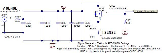
Figure 1 is an example of a power-supply output test setup where I monitored the response to a large step load on the output and also had the oscilloscope monitor the dynamic load current across a low-value resistor. I used a signal generator to drive the desired step load size with the desired rise and fall times and sensed voltage with a 50Ω cable attached to J502. The 50Ω R527 dampens any reflections on the cable. I used the tip-and-barrel approach to sense current across R500 with a 10x oscilloscope probe.

Figure 1: Test setup

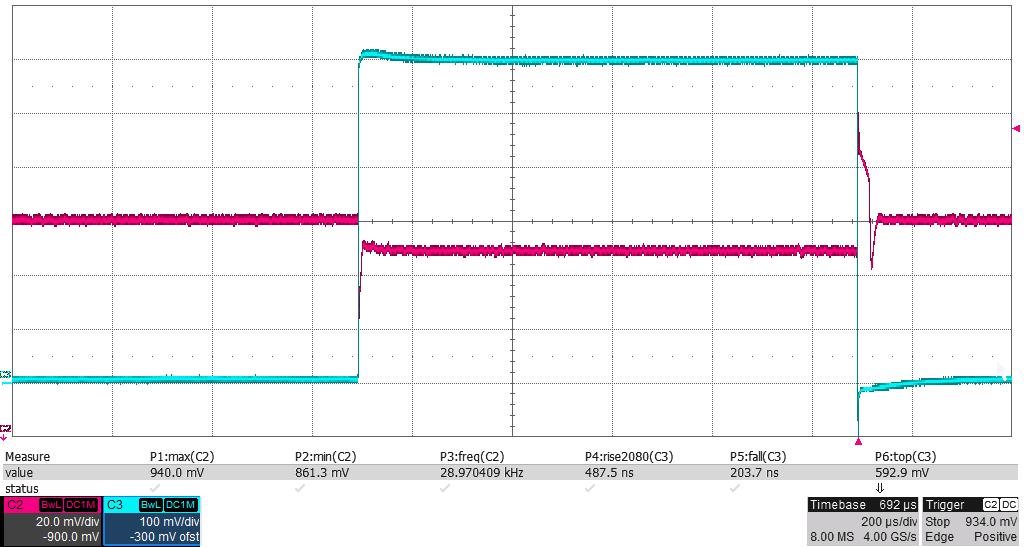
Figure 2 shows both the sensed voltage and sensed dynamic load current on the same oscilloscope when applying and removing a 59A pulse load.

The application requirements are that VOUT (the red trace on the oscilloscope/J502 in Figure 1) stays within a 855-945mV range under both load step and load dump. Dynamic current is measured across a 10mΩ resistor (R500 in Figure 1) tied to ground and is the green trace shown in Figure 2.

Figure 2: Step-load and load-dump response from 2A to 61A with dynamic current sense while connected to the oscilloscope

Based on Figure 2 and looking at the channel two red trace showing Vout, the voltage output drops to 861mV when applying the load step, then stabilizes at 889mV with the higher load. Upon removal (dump) of same added load, the voltage output peaks at 940mV before stabilizing at 900mV. Thus, the voltage output stays within the 855-945mV limits, and the test “passes.” Looking at the channel three green trace showing the voltage across the 10mΩ current sense resistor, the dynamic load goes from 0A to 593mV/10mΩ, or 59A and back to 0A.

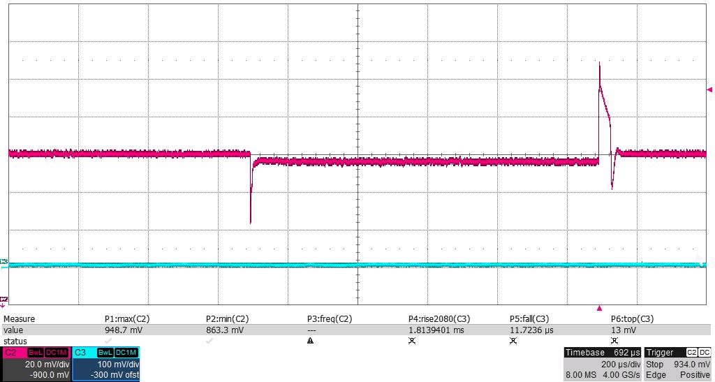
Disconnecting the current-sense probe from the oscilloscope shows a different voltage waveform on the output. See Figure 3.

Figure 3: Same dynamic response at VOUT with the current sense disconnected from the oscilloscope

Based on Figure 3 and looking at channel two red trace showing output voltage, the voltage output drops to 863mV when applying the load step, then stabilizes at 896mV with the higher load. Upon removal (dump) of the same added load, the voltage output peaks at 949mV before stabilizing at 900mV. Thus, the output goes above the 945mV limit and the test “fails.”

Off-site test experience

Testing with an off-board “load slammer” and trying to monitor both the output voltage on the main board and the dynamic load on the slammer made the dynamic response look very poor. When I removed the current-sense connection from the oscilloscope, I saw a good dynamic response. There, the current-monitor connection created a false fail.

If you are going to monitor both current and voltage on the same oscilloscope, you will need either an oscilloscope with fully isolated inputs or a dynamic load with sense resistor ground right at the voltage-ripple monitor. For the first option, you’ll also need two sets of differential probes with good input isolation.

Stay tuned for an upcoming blog highlighting a design with a dynamic load test interface which will allow monitoring both voltage and dynamic current at the same time without differential probes. 

Additional resources

What’s next for Advanced Driver Assistance Systems?

$
0
0

As the sector general manager of TI’s Advanced Driver Assistance Systems (ADAS) team, I’ve seen an incredible evolution in the role this technology plays in delivering an all-around safer, more comfortable and more informed driving experience.

At TI, our family of Systemon–Chip (SoC) ADAS products and the complete ecosystem of analog components we offer around it provide scalable and open solutions, common hardware and software architecture for a variety of applications including camera-based (front camera, rear and surround view systems, mirror replacement, driver monitoring) applications, as well as radar-based (blind spot warning and collision avoidance)  and sensor fusion systems.

Yet despite the array of systems we offer, one thing hasn’t changed – the driver. No matter how many new ADAS solutions we develop, human drivers are the one variable that can be hard to quantify.

That’s about to change in a big way, however. Ready or not, autonomous vehicles, fueled by an array of advanced sensor technologies and digital processing power are already in various stages of development.

According to research firm IHS Automotive, there will be 76 million various levels of autonomous vehicles on the road globally by 2035. The implications of having this many autonomous vehicles on the road will redefine the daily commute, and rewrite expectations of our customers and original equipment manufacturers (OEMs).

Making autonomy work

An array of new technology and solutions are the base to deliver a successful autonomous vehicle experience. The unprecedented levels of automation will require more sensors in order to perceive a complex driving environment. In turn, this will create far greater data volumes to be processed and distributed across networks in real-time, with the utmost reliability.

All of this will have to function seamlessly, under extreme environmental conditions. It’s clear to me that future of ADAS designs will need some key features to be successful.

First, size, efficiency and performance will continue to rule the day, just as they do now. Smaller, more efficient,yet powerful ADAS applications will only become more critical as autonomy drives up requirements for far greater amounts of data capture. Processing all of this data to make the correct decisions in real time is another hurdle, as is the  effort to get the data from the sensors to the processor.. And of course, the solution has to make financial sense in order to be commercially viable in everything from luxury to entry-level vehicles.

Rethinking the role of ADAS

Perhaps one way to address these challenges is to start thinking about ADAS as more than the sum of its parts. Right now, ADAS subsystems often work independently of each other. For example, adaptive cruise control doesn’t necessarily know what blind spot detection is doing.

What’s needed is a more holistic ADAS approach where all sensors across the automobile are part of a more connectedcollective, making smarter and more reliable decisions. At TI,we are  creating an ecosystem of products and solutions that are purpose built to support fast-changing needs of the automotive market today, and for future generations.. We’re also working closely with our customers to help lead the way in the inevitable evolution toward the day when autonomous vehicles are the norm, not the exception.

Clearly, ADAS is an exciting market space that is always changing. From comfort and safety, to fuel efficiency and connectivity, however, I think we’re at a particularly interesting time in the automotive world. Nothing less than the entire concept of individual transportation is changing, and I’m happy to be a part of this exciting transformation. 

Why enter the India Innovation Challenge? Let previous winners tell you

$
0
0

As the deadline for the India Innovation Challenge Design Contest (IICDC) 2016 is approaching, we wanted to help our participants benefit from the experiences of the last year’s contestants. And who better to speak to than Rakshit Ramesh, Karthikeshwar Varma & Anoop Kulkarni, winners of the 2015 TI IICDC? They came up with an idea to address a serious problem of road accidents in India and impressed the judges with their vision and the execution. (See their project)

 
1. What was your experience in IICDC 2015?

Rakshit: The highlight of the contest was receiving an award from Late Former President of India, Dr. APJ Abdul Kalam. Also, our project meant a lot to me because it was inspired by a real life incident. One of my neighbors had a road accident due to low visibility. We wanted to solve this by designing a radar system for cars. We had prior experience using TI controllers and integrated circuits (ICs) and we used TI’s website to find relevant components and technical information. Identifying the right components was the key, as once you are in the design cycle it is difficult to make changes.

2. How has TI helped you during the contest?

Anoop: We received technical support through workshops and a clear understanding of the contest from TI. During semifinals and finals we got to interact with TI employees who shared industry insights and other technical information, thereby helping us improve our designs.


3. How did the contest help you acquire new skillsets and make a mark in your career?

Karthikeshwar & Anoop: We learned a variety of new skills like…

    • Teamwork as electronics experiments often don’t go according to the plan.
    • Time and risk management as we had to juggle between our coursework and contest
    • Presentation skills as we needed to present our work to judges at every stage.

Rakshit: I learned the process of product development like how to design a circuit board for testability and ensure it is debuggable. Everywhere I go, I identify myself as a winner of the TIIC! (laughs). It’s a one of a kind contest where the competition is so fierce that winning it has definitely helped me get an edge over others. We are all working as research assistants in IISc Bangalore.

4. This year, the top 10 teams will be converted as start-ups. Your advice for the participants?

Rakshit: It’s a wonderful opportunity. When we won, we were looking for investors and a marketplace for our idea. You can create products, but it needs to be marketable. Undergraduates often lack managerial skills – this is where IIMB can play a crucial role. Funding from DST is also a huge advantage as it is like an official stamp of approval for student projects.

Karthikeshwar: Over a year, you have a chance to grow professionally as well as personally; by the end of the contest, you acquire technical and soft skills that are essential for being an engineer. I would highly recommend every engineering student to participate in the India Innovation Challenge.

If you have an innovative idea, a dream to create something new, and the ambition to make a difference, then we invite you to participate in the IICDC 2016. Enter the India TI Innovation Challenge design contest by September 30, 2016 for your chance to launch your own startup.

The fourth industrial revolution with Mesh

$
0
0

The third Industrial Revolution introduced electronics and information technology to automate the production process (e.g. robotics arms manufacture most of our products).

Today, we experience its fourth stage. This revolution is characterized mainly by fusion of technologies enabling inter-communication between different production line machines. We can see more and more smart solutions taking place in the traditional industry products such as:

  • Machine to machine (M2M) inter-communication allows utilizing the manufacture line process.
  • Smart helmets that can operate in one network and make the work environment much safer.
  • Using one network for an indoor location services platform.
  • Smart Grid infrastructure allowing a network of meters to read and send data over Wi-Fi®.

 The Texas Instruments (TI) WiLink™ 8 mesh solutions open many new opportunities for the industrial sector by enabling this M2M communication. Having all the machines communicating with each other, sharing information and reporting back data is a major step forward in the next industrial revolution.

The main advantage of using the mesh solution for the industry sector over standard Wi-Fi coverage is by lowering the infrastructure cost. With mesh, no need to deploy many routers over a large territory in order to have the required coverage. Each device can inter-communicate with all the devices around it. The mesh network also has the capability to self-healing, meaning even if one of the peers is dropped the network recovers. This is a secure, easy to deploy and always connected network.

When it comes to wireless connectivity, TI’s mesh solution makes all of it possible. What other applications might be possible with the Mesh network? Let us know in the comments below. 

Additional resources:

How level shifters enable the transition to low-voltage processors in industrial environments

$
0
0

Consumer, computing, personal electronics, enterprise networking, automotive and industrial use cases are moving rapidly toward lower-voltage processor and microcontroller technologies. The advantages of lower-voltage processor-based systems – higher levels of energy efficiency, longer battery life, improved thermal performance, reduced production costs and lower cost of ownership – are powerful incentives for system designers. Today, I am focusing on the benefits industrial system designers gain from moving to low voltage processors.

Given that industrial applications areas such as building automation, factory automation and smart grid by nature need to support higher-voltage peripheral devices such as connected sensors, actuators, field buses, motor-drive units and many other components operating at higher-voltage domains, choosing a lower-voltage processor-based design can become especially complicated. The major challenge that industrial system designers face when integrating higher-voltage components with lower-voltage processors is bridging the data interfaces between components that operate at different voltage levels. You cannot simply connect the data and control interfaces of devices on different voltage rails together and then expect them to interoperate.

Industrial system designers resolve voltage-level differences in data and control interfaces by level shifting (also known as level translating) the interfaces to common voltage levels so that the devices can interoperate as expected. System designers have historically used multiple discrete components such as transistors and resistors to implement level-shifting schemes within their applications. However, today’s modern designs are using integrated level-shifting solutions like integrated circuits (ICs), which provide a greater level of flexibility, scalability and robustness when compared to discrete implementations.

The value of integrated level-shifting solutions becomes very clear as the number of data lines that need to shift increases for a given implementation. For example, level shifting an 8- or 16-bit interface would require 20 to 50 discrete components compared to a single level-shifter IC. In addition, the discrete solutions would require a greater amount of engineering effort to manage component-to-component performance variability, such as a propagation delay over temperature and its associated impact on system timing. The large increase in component count, associated with discrete implementations, also increases the probability of system reliability issues. As industrial systems become more sophisticated, integrated level-shifting solutions are becoming an important component of a design engineer’s toolbox. Figure 1 offers a few examples of integrated level shifting.

 Figure 1: Example of step down and step up level translation

Integrated level-shifting solutions are available in a wide array of bit widths, data-rate ranges, current drive capabilities, package options and other application-specific functions. For example, TI’s portfolio of level-shifter devices contains several different types of functions to address almost any application requirement. Common level-shifter types include auto-direction-sensing level translators; bidirectional multi-voltage-level translators; dual-supply direction-controlled push-pull level translators; auto-direction-controlled push-pull level translators; and finally, application-specific level translators. Figure 2 shows some examples of the different level-shifter types.

Figure 2: Example of different level translator types

In the next installment of this two-part series, we will explore how to select the appropriate translator solution and rules of thumb for implementing level translators in industrial applications. In the meantime, to learn more about voltage-level translation, log in to leave a comment or visit voltage level translation portal.

Additional resources

Viewing all 4543 articles
Browse latest View live


<script src="https://jsc.adskeeper.com/r/s/rssing.com.1596347.js" async> </script>