Quantcast
Channel: TI E2E support forums
Viewing all 4543 articles
Browse latest View live

The difference between hysteretic-mode converters and traditional regulators

$
0
0

When designing a power circuit, many of the selections available on the market, such as traditional voltage and current-mode regulators, look similar. You know it will do a certain job - for example, step-down DC/DC conversion - but you may not know how the many choices compare to each other.

If you haven’t considered it before today, my recommendation is a hysteretic-mode converter.
Hysteretic-mode converters are branded in many different ways, including D-CAP™, D-CAP+™, D-CAP2™, D-CAP3™, constant-on-time, or DCS-Control.

When you’re deciding between the many choices, you probably do what I do; search online and find a comparison report, or find a site with reviews to see recommendations and complaints.

To help you in this effort, I authored a 3-part series of articles “Hysteretic-Mode Converters Demystified” aimed at comparing a hysteretic-mode step-down switching regulator with traditional voltage-mode and current-mode regulators. This series in Power Electronics Technology magazine is based on lots of measurement data behind the scenes (see example in Figure 1) and includes unbiased comparisons as much as possible. 

Figure 1. Screenshot of the many measurement plots I compiled for the comparison.

I kick off part 1 of the article series “Hysteretic-Mode Converters Demystified” by reviewing basic operation differences of hysteretic-mode, voltage-mode and current-mode converters. This part illustrates the fundamental differences and also points out similarity of converters.

In part 2 “Voltage and Current Mode Control,” I compare large signal load and line transient behavior. This section reviews the many technical plots pictured above to highlight the differences between control modes.

In part 3 “Regulator Stability,” I examine small signal behavior and stability.  This part reviews three different small signal measurements (Bode plot, output impedance and small signal load transient) so you can get good idea of how hysteretic-mode converters perform.

I hope you enjoy the article series and I look forward to answering any questions you may have. If you are a more visual learner, view the seven-part video series based on these articles “Fixed Frequency vs Constant On-Time Control of DC/DC Converters”.

Additional resources:


Eliminating noise from the factory floor

$
0
0
Industrial automation systems use microprocessors, digital signal processors (DSPs) and a network of sensors to control electromechanical processes. These components are highly sensitive, yet operate in environments filled with electrical noise caused...(read more)

RF sampling: analog-to-digital converter linearity sets sensitivity

$
0
0

In my previous post, I discussed details of third-order intermodulation (IM3) linearity parameters in active devices. Now let’s apply those techniques and parameters to a real RF-sampling receiver.

The key active components in the lineup are the low-noise amplifier (LNA) and the analog-to-digital converter (ADC). The receiver antenna is “looking at the world” (that is, the entire frequency spectrum). Interference signals picked up by the antenna create intermodulation distortion within the active devices of the receiver that may land within the band of interest. Once the distortion lands in-band, there is no opportunity to filter it out. Filtering the interference signal before it hits critical components is the first line of defense. The second line of defense is to ensure that the active components’ linearity performance is stout enough to handle the interference signals that get through the filtering.

Figure 1 is a block diagram of an RF-sampling transceiver operating in frequency duplex division (FDD) mode. Recall that in FDD mode, the transmitter and receiver operate simultaneously. The transmitter operates at very high powers, in the 10-100W range (40-50dBm). The diplexer filter passes the high-power transmitter signal to the antenna and isolates that signal from the receiver. The diplexer filter is a large cavity filter able to provide sharp selectivity and very low loss. It is also very expensive. One known interference signal is the bleedthrough of the transmitter signal through the filter to the receiver. If the transmitter operates at 40W (46dBm) and the cavity filter provides an impressive 95dB of selectivity, the interference signal at the receiver input is still -49dBm, which is fairly high.

Figure 1: RF-sampling transceiver block diagram

A myriad of other unpredictable sources of interference can impact the receiver: other mobile users close to your receiver, competing communication signals or other high-power transmitters. Having one of these sources at the proper frequency, combined with the transmitter bleedthrough, generates an intermodulation distortion product that falls within the band.

Let’s investigate an example to illustrate the situation. Figure 2 shows the spectrum of a receiver operating in the 1.96GHz UMTS telecom band. The transmit band is located only 60MHz above, centered at 2.14GHz. Some of the transmitter power will seep into the receiver. If a high-power interference signal hits the receiver at around 2.32GHz, then the low-side intermodulation product lands right inside the receiver band. The input filtering is the first line of defense, but it cannot completely eliminate all of the interference. The second line of defense is to ensure that the cascaded linearity performance of the receiver is good enough to pass sensitivity requirements in the presence of blockers.

Similar to the cascade analysis shown in my previous post about noise, adding input intercept point parameters to the lineup analysis shows how the combination of each device in the lineup contributes to overall system performance. Third-order input intercept point (IIP3) is the “yang” to noise figure’s “yin.” With noise figure, higher gain and less loss yield better noise performance. With IIP3, lower gain and more attenuation tend to yield better linearity performance. You must strike the proper balance within the lineup to ensure proper signal reception at the lowest sensitivity level and in the presence of blockers. 

Figure 2: IM3 distortion falling within the receiver band

Equation 1 calculates the cascaded two-tone IIP3 performance. The “i” element represents the current stage and the “i-1” stage represents the subsequent stage. The “Attn” terms represent any filter selectivity at the adjacent and alternate tone locations.

The 14-bit, 3-GSPS ADC32RF45 ADC is an excellent choice for communications systems. As previously discussed, it has a low-noise spectral density output. Just as important, it has high linearity performance. Figure 3 shows one example of a possible interference situation. Two tones are placed just outside the telecom receiver band. The tones create a third-order intermodulation product that lands within the receive band. The tones in this case represent a 10MHz-wide jammer signal just outside the desired receive band. The third-order intermodulation delta (IMD3) parameter reflects the relative power of one fundamental tone to one third-order intermodulation tone.  The IMD3 performance in this example is about -71dBc.

Figure 3: IMD3 performance with interference tones just outside the desired band

Figure 4 shows another interference scenario with transmit (TX) bleedthrough at 2.14GHz and jammer at 2.32GHz. The IMD3 performance is about -79dBc. The IIP3 performance calculated from the measured results referenced to a 50Ω system is used in the cascaded lineup analysis. Note that small changes in filtering and gain have a large impact on performance. This is due to the 3-to-1 ratio inherent in third-order intermodulation. Judicious use of attenuation or increased filtering in the proper place makes for a significant improvement in system performance.

Figure 4: IMD3 performance with transmit bleedthrough and blocker signal

Check back next month, when I will discuss how to use clock phase-noise measurements to analyze RF- sampling data converter performance. Be sure to sign in and subscribe to Analog Wire to get my next post delivered right to your email inbox.

Additional resources

How we’re charging up the future of electric and hybrid automobiles

$
0
0

Imagine a world where self-driven, zero-emission electric vehicles (EVs) communicate among themselves and with roadway infrastructure. Imagine cities filled with cars that can safely deliver passengers, and then direct themselves to parking spaces with inductive pads to quickly recharge until they are summoned again.

Fueled by a series of advances in automotive electronics now underway at Texas Instruments, this vision for the future of the automobile is rapidly becoming science fact instead of science fiction.

The growing influence of electronics in automobiles

From the electrification of vehicle engines to increased automation, safety, comfort and convenience, advanced electronics are the key factor enabling many of the improvements in automobiles.

At the engine level, auto manufacturers and customers are increasingly turning to various forms of EVs, hybrid-electric vehicles (HEVs), and electronically assisted combustion engines to improve gas mileage and lower emissions cost-effectively.

EVs will continue growing slowly but steadily in number, approaching five percent of overall auto sales worldwide by 2025, according to market analyst firm IHS Automotive. Hybrid electric and gasoline combustion motors in that same year will amount to some 22 million cars, about 20 percent of cars sold worldwide.

What’s driving the EV revolution?

Not only are EVs reducing fuel consumption and emissions – they are also helping manufacturers develop the supporting technologies needed for electrification, while giving consumers time to become accustomed to them. Governmental mandates as well as market demand will determine the pace of this transition.

Increasingly, integrated circuits (ICs) that sense conditions, drive actuators, convert signals, communicate among vehicle systems, and decide what to do—often without intervention by the driver—are key automotive components.

ICs that function in vehicles must operate under extreme conditions of voltage, current, temperature and vibration, and they must operate reliably to keep the equipment and occupants safe.

At TI, we offer a broad portfolio of innovative solutions that enable automakers to design and build more efficient, safer and more comfortable cars that are easier for their customers to operate.

As the revolution in transportation continues, new introductions in auto electronics are continuing to make cars more fuel-efficient, safer and convenient. Electrically assisted combustion engines, hybrids at various levels, and full EVs are all making a change in emissions that cut down on pollution locally and greenhouse gases globally.

Automated driving and EVs will change the operation of vehicles, especially in cities, bringing new business models that help provide low or zero emissions and customized transportation for millions.

I’m excited to be at TI, where we will continue to play an important role in bringing electronics to vehicles today while driving toward an automotive future that is safer, more convenient and environmentally friendly.

How does precision lead to automotive safety?

$
0
0

Semiconductor content keeps increasing in automobiles, thanks to the number of sensing technologies. In a span of ten years, the number of sensors has increased steadily across all sensor types. This trend is likely to continue, as more features, which were previously only offered in luxury vehicles or available for purchase after-market, become crucial and in some cases mandated by governing bodies.

Advanced driver-assistance system (ADAS) solutions are one of the fastest-growing automotive sectors; the sector is expected to grow by 10 percent from 2015 to 2020, according to a forecast by Strategy Analytics. Even designers of entry-level models now expect ADAS features. As a result, car manufacturers try to meet demand by implementing these features even in entry-level models.

The most popular ADAS applications consist of collision avoidance, lane-departure detection, park assist and adaptive cruise control. Depending on geographical area, some applications may be more desirable than others. For example, in densely populated regions, consumers are more likely to want collision warning in their cars, whereas drivers in mountainous areas may feel the need for dynamic lighting.

In cities like Shanghai, Moscow, Mumbai or Istanbul, drivers may want object detection with a high level of accuracy. In crowded cities like these, pedestrians, motorcycles and buses can emerge at any given moment. To assist the driver, the car must be able to respond quickly, based on an accurate measurement of the distance between the car and the object.

Object-detection applications usually require precision circuits, such as operational amplifiers (op amps), which serve as the fundamental building blocks of a signal chain or analog front end that control the rest of the circuitry in these driver assistance systems.

Precision devices, such as the OPA2320-Q1 op amp that has been used into many ADAS designs, provide a low offset voltage and wide bandwidth, which help eliminate system calibration. Because system calibration can involve complex algorithms or even a power-hungry DSP in some design configurations, designers can save on software costs and design time by using precision analog integrated circuits (ICs). 

While a low offset voltage is necessary to achieve overall system accuracy, the op amp’s wide bandwidth plays a crucial role for settling time. The op amp should settle within ½ LSB of the data converter it drives in order to maintain adequate signal acquisition and integrity.


Figure 1: Settling time of OPA2320-Q1 with ±2V input step at a gain of +1

If you’re designing automotive applications, be sure you’ve subscribed to the Behind the Wheel blog to receive more system-level advice and insight on trends.

Additional resources

How to fix your simulations when the macromodel’s voltage noise doesn’t match the datasheet

$
0
0

When responding to questions posted on TI E2E™ Community forums, we frequently run simulations using TINA-TI™ software, a SPICE-based simulation program. Since we are always in the process of updating our simulation models, we sometimes run across SPICE models that are old, outdated or incorrect when modeling performance parameters.

One recent example involves the voltage-noise density of the OPA2333 macromodel. Unfortunately, we found that the model’s voltage-noise density curve was less than that given in the data sheet. So in this blog post, I will show you how to verify an operational amplifier’s (op amp) voltage-noise density curve and correct it if necessary.

First, you need to know how to generate a voltage-noise density curve using TINA-TI software. In this example, I will use the OPA2333 macromodel and schematic shown in Figure 1.

Figure 1: TINA-TI test bench for voltage-noise density

The output noise in this configuration uses the op amp with no gain, filtering or other factors that would change the voltage noise over frequency.

To simulate the output noise, select Analysis > Noise Analysis, and tick the Output Noise check box shown in Figure 2.

Figure 2: How to find noise analysis for output noise


Figure 3: Simulated OPA2333 voltage noise


Figure 4: OPA2333 voltage noise according to the data sheet


You can add noise to the macromodel by inserting a voltage-noise source in the schematic.

To get the voltage-noise source, go to File > Open Examples. Select the Noise Sources folder and open the TINA Noise Sources.TSC file shown in Figure 5.

Figure 5: Finding the voltage-noise source and equivalent op amp noise model

Now, copy and paste the voltage-noise source from the noise-source schematic into the testing schematic and add it to the noninverting input, as shown in Figure 6.

Figure 6: Testing schematic for input-voltage noise with a voltage-noise source

Double-click on the noise source and select Enter Macro. A tab will open showing the netlist of the voltage source; see Figure 8.

Since the OPA333 is a chopper op amp and has no flicker noise, you do not want to add flicker noise to the voltage source. Find the parameters NLF and FLW and change them to 0 and 0.1, respectively. This sets the flicker noise to 0 nV/ √ Hz at 0.1Hz. You will also need to adjust the broadband noise so that the root sum square (RSS) noise is equal to the value you want. In the netlist, this value is represented by the parameter NVR.

In Figure 7, I solve for the desired broadband voltage. Figure 8 shows the updated parameters inside the netlist. 

Figure 7: Solving for the broadband voltage-noise value


Figure 8: Netlist of voltage-noise source

Running the noise analysis again (Figure 9), you can see that the voltage noise is now the same value shown in Figure 4.

Figure 9: Corrected op amp voltage noise

Note that this process only works when your macromodel’s voltage-noise density curve is less than that given in the data sheet because RSS noise can only be added. If your macromodel’s voltage-noise density curve is more than that given in the datasheet, the TI Precision Labs on-demand training series includes a short video on how to create your own accurate macromodel for noise simulations. You can find the video here*.

Remember, trust your SPICE models, but verify that they are correct. Simulations can take you far, but they need to simulate correctly to produce meaningful results.

Additional resources

*This requires a myTI log-in. 

Four design tips to obtain 2MHz switching frequency

$
0
0

Designers must meet many electromagnetic compatibility (EMC) requirements for automotive applications, and choosing the right switching frequency (fsw) for the power supply is important to meet these requirements. Most designers select an fsw outside the medium-wave AM broadcast band – typically 400kHz or 2MHz, where electromagnetic interference (EMI) must be limited. The 2MHz option is desirable for many reasons, so in this post, I’ll provide some key considerations when trying to operate at 2MHz using TI’s new TPS54116-Q1 DDR memory power solution as an example.

The first and most important consideration when operating at a 2MHz fsw is the minimum on-time of the converter. In a buck converter, when the high-side MOSFET turns on, it must stay on for a minimum on-time before it can turn off. With peak current-mode control, the minimum on-time is usually limited by the blanking time of the current-sense signal. The highest minimum on-time of a converter usually occurs at the minimum load condition and there are three reasons for this.

  1. There are DC drops in the circuit at heavier loads, increasing the operating on-time.

2. The rise time and fall time at the switching node. During the dead times (the time between when the low-side MOSFET turns off to when the high-side MOSFET turns on and between when the high-side MOSFET turns off and the low-side MOSFET turns on), the current through the inductor charges and discharges any parasitic capacitance at the switching node. At light loads there is less current in the inductor, so the capacitance charges and discharges more slowly, causing longer rise and fall times at the switching node. These longer rise and fall times cause the effective pulse width at the switching node to increase.

3. Low-to-high dead time. When the low-side MOSFET turns off and before the high-side MOSFET turns on again, the current through the inductor charges the voltage at the switching node until the body diode of the high-side MOSFET clamps the switching-node voltage. As a result, the switching node is high during the low-side MOSFET off-to-high-side MOSFET on dead time. Since the switching node is high during this time period, the low-to-high dead time adds to the effective minimum pulse width. In Figure 1, you can see that although the on-time is the same, the pulse width is larger.


Figure 1: Pulse-width at full load vs. no load

The second consideration when trying to operate at 2MHz is the minimum input voltage (VIN) to output voltage (VOUT) conversion ratio. This is related to the minimum on-time of the converter because this ratio sets the on-time at which the converter needs to operate. For example, if a converter has a minimum on-time of 100ns and operates at 2MHz, using Equation 1 the minimum conversion ratio (Dmin) it can support is 20%. If a given VIN-to-VOUT ratio requires an on-time less than the minimum on-time, most converters enter a pulse-skip mode to keep the output voltage regulated. When pulse-skipping, the fsw varies and can cause noise in frequencies where noise needs to be limited.

                            (1)

In automotive applications where the power supply connects to a battery, the on-time must support conversion from a typical VIN range of 6V to 18V. Using equation 2 with an 18V maximum input and 20% conversion ratio, the minimum output voltage is 3.6V. When directly connected to the battery, large voltage spikes can occur (such as during load dump) that exceed this typical range. Depending on the requirements of the application, the converter may or may not be allowed to pulse-skip during input voltage spikes.

                                 (2)


A regulator connected to a 3.3V or 5V rail can more easily operate at 2MHz. For example, the TPS54116-Q1 has a maximum minimum on-time of 125ns, so at 2MHz the minimum duty cycle is 25%. The minimum output voltage supportable from a 3.3V input is 0.825V; from a 5V rail it is 1.25V. A full analysis for the minimum output voltage in a given application should also include the tolerance on VIN and fsw.

The third consideration when trying to operate at 2MHz is AC loss in the inductor. AC loss increases with fsw so it needs to be considered when choosing an inductor for 2MHz. Some inductors use a core material designed for lower AC losses to give better efficiency at higher frequencies. Most inductor vendors provide a tool to estimate AC loss in their inductors.

The fourth consideration when trying to operate at 2MHz is the tradeoff between size and efficiency. When selecting the fsw for a DC/DC converter, you must make a trade-off between size and efficiency. The inductor size and some converter losses increase with fsw. Comparing 400 kHz to 2MHz specifically, a 2MHz design will use 5x smaller inductance but have a 5x larger switching loss. A 5x smaller inductance means a smaller inductor size.

The two main losses in a converter related to fsw are switching loss in the high-side MOSFET and dead-time losses. Equation 3 is a basic estimate of these loses, which you can use to further analyze the effect of increased loss with higher fsw. For example, with a 5V input, 4A load, 3ns rise time, 2ns fall time, 0.7V body-diode drop and 20ns dead time, the estimated power loss is 325 mW at 2MHz and 65mW at 400kHz.

   (3)

Extra power losses cause a higher operating junction temperature. Using equation 4 with RθJA = 35°C/W from the TPS54116-Q1EVM-830, the integrated circuit’s junction temperature will increase by only about 9°C. The thermal performance can vary with different PCB layouts.

  (4)

Just because the data sheet has 2MHz on the front page does not mean that 2MHz is achievable across all operating conditions. Switching at 2MHz has its advantages and disadvantages, and there’s always a trade-off between the size of your DC/DC converter solutions and efficiency. Order the TPS54116-Q1EVM-830 evaluation module and start your 2MHz design in WEBENCH®Power Designer now.

Why should you count squares?

$
0
0

When I studied electrical engineering at the university, math was extremely important. My math professor was so diligent that he would attend other classes to see if the lessons involved math that he needed to teach us to make our lives easier. More than once he changed his lesson plans to incorporate math topics from the other classes, so I was very grateful that he was so passionate.

When I became an application engineer for power supplies, I quickly learned that there are parasitics in all components. The formulas to calculate the best-fitting component became more and more complicated when including these parasitics. Sometimes a simplified formula or even a rule of thumb helped me get at least close to a result, enabling me to find the best-fitting available component through trial and error.

One issue where I could never use math, however, was when deciding about the best layout. I still don’t have a really good simulation tool that can predict exactly which layout is the best fit for the specific power supply I want to design. My dilemma gets even worse if the IC includes several converters, like LCD (Liquid Crystal Display) or OLED (Organic Light Emmiting Diode) display power products. The parasitics of a layout not shown in the schematic do influence the performance of a circuit and can even cause hazardous failures in a power supply. So it is important to do the layo=ut right the first time.

One parasitic effect to keep in mind when doing a layout is the trace or plane resistance. Here is a rule of thumb that I’ve learned to estimate it:count squares.

I learned about this rule the first time I laid out a power-supply design. I remember being somewhat puzzled because I could not believe that it could be so simple, but it is; I even can use math to show you that it’s true.

Equation 1 calculates the resistance of copper:

                            (1)

Figure 1 shows a piece of copper on top of a printed circuit board (PCB).

Figure 1: Copper piece carrying current in a power-supply design

Assume the current is flowing from left to right along l  and distributes evenly in area A. In this case, Equation 1 becomes Equation 2:

                            (2)

You can see now that the resistance of this piece of copper is independent of the dimension l  . So now the formula for resistance on a PCB changes to Equation 3:

                 (3)

Where r is the well-known specific copper resistance and the production specification of the PCB defines the thickness of the copper.

This means that regardless of how big l  is, the resistance stays the same. For a layout person this is really good to know, because if you want to make the resistance as small as possible, make it as wide and as short as possible.

You can determine the thickness of copper on a PCB from the requested production parameter (see Table 1) and estimate the resistance of a specific piece of copper in the layout by counting squares.


Table 1: Copper Thickness and resistance based on the production parameter Copper Weight
 

Assume your piece of wire looks like Figure 2.


Figure 2

Divide it into squares, as shown in Figure 3.


Figure 3


Say that you can fit 10 squares into your piece of wire, like in Figure 3. If you are using 1oz copper on your PCB, the resistance of this piece of wire is roughly 5mΩ. If a current of 1A is going through this piece of wire, the voltage drop from one end to the other end will be 5mV. Assuming a voltage of 1V on one end, the voltage on the other end is 0.5% smaller – and this is just one piece of wire. Double the width of your wire and you halve the resistance.

So even if it is relatively easy to calculate the parasitic resistance, using my eyes and estimating the number of squares that fit into the wire made it a lot easier for me. Let me know how this works for you in the comments below!Check out the LCD/OLED display bias solutions offered by TI and share your results in the LCD/OLED Display Bias Solutions forum on the TI E2E™ Community.


Engineer returns to African country he once fled to inspire village students, improve education

$
0
0

Innocent IrakozeThe arc of Innocent Irakoze’s life changed dramatically one morning when he stood outside a school for refugees in Tanzania and saw his name at the top of a list of students who had failed sixth grade.

He wept. And then he made a decision that changed his life.

“When I saw my name on that list, I developed a different mindset,” he said. “I decided right then that I would never fail again and that I would be the first in my class from then on.”

In addition to a newfound determination to succeed, the shock of failure that day later blossomed into passions for education and for helping others succeed.

Those passions came together in June when Innocent took an extended vacation from TI to visit his family in Africa for the first time in many years – and used $5,000 he had raised to deliver school supplies to about 3,000 elementary-age students in his village in northern Burundi. That initial donation has grown into a plan to support the educational dreams of Burundian students through a nonprofit organization he is establishing.

“Being in the school recently made me very emotional,” Innocent said. “Burundi is one of the poorest countries in the world. Twenty-something years ago, I was sitting where those kids were sitting. A lot of those kids don’t have shoes. A lot of them don’t eat before they go to school or after they go home. I wanted to show them that somebody cares about their education and that education can take them far.”

(Please visit the site to view this video)

Almost a decade after he came to the United States, education has carried Innocent far. Today – after earning a high school degree, an associate’s degree and a bachelor’s degree in electrical engineering – he works at our company as a product marketing engineer in Dallas. He hopes to continue his education with a master’s degree in business administration.

“Innocent’s story is like a movie or a book, but it’s real life” said Sergio Perez-Ruiz, a friend and colleague. “Some people went through a lot to get where they are. His story about refugee camps, war and not knowing whether he would make it to the next day makes me grateful for where I am. Innocent’s path was rocky, but it shows that if you really want something you can make it happen.”

Refugees on the run

Most of Innocent’s life has been hard by any measure. Ethnic fighting and fear marked his early years, and he spent most of them as a refugee.

A coup d’etat sparked tribal brutality in Burundi the year he was born, 1987, and his family fled as refugees to the neighboring Democratic Republic of Congo, hardly a bastion of safety itself. Innocent’s family moved back and forth between refugee camps and their home for the next decade, avoiding rebel groups during a series of deadly ethnic conflicts in Burundi and eastern Congo.

Innocent (background) and several Burundian children at a village school

One of his earliest memories is of fleeing across the Rusizi River from Burundi to Congo in 1991. The nearest bridge was far away, so his parents made a crude raft by tying four banana tree logs together. His mother was pregnant with his younger brother, and Innocent rode in a sling on her back.

The massacres began again in 1993, when the East Africa nation’s president was assassinated. Estimates put the death toll in the country at about 300,000 in subsequent years. The next president was killed in 1994, when rebels shot down the plane carrying him and the president of Rwanda. Another coup d’etat followed in 1996, and two years later much of the nation’s population fled to refugee camps.

“We didn’t have any place to go,” Innocent said. “If we stayed in Congo, we were going to die. If we went to Burundi, we had the same chance of dying. So my dad took a chance and we went to Burundi. Things were bad. At one point I got lost for a few days and my parents thought I was dead. A lot of people were shot to death, but no one in my family was shot.”

During a period of relative calm, Innocent attended first and second grade in the bare-bones school in his home village – and it was there that he returned with school supplies in June. But he spent the next few years attending schools as a refugee in Congo.

Redefining his life

A turning point came in August 2001. Innocent had been living with an aunt and attending school in Congo. During a school break, he visited his parents in Burundi.

Violence in eastern Congo was on the rise again – rebels brought death with them from their mountain hideouts into the village where he had been living with his aunt – and his parents convinced him that he would have more opportunities and be safer living near his older brother in a refugee camp in Tanzania.

His sister accompanied him on a long bus ride to southern Burundi, and they walked across the border together.

 Burundian children at the village school Innocent once attended

It was at that camp that he took a standardized test required to advance from sixth to seventh grade. Although he was a good student and spoke Swahili, French and his native language, Kirundi, the school he attended in Congo didn’t teach him to read or write in Kirundi.

Because he failed Kirundi and other areas of the standardized test, he was forced to repeat sixth grade.

“I took failing the test as a challenge,” he said. “I decided that I would be first in every class after that, and I was first in every class until I came to the U.S. Achieving that goal was a huge accomplishment. I was able to redefine my life, redefine what I wanted to do. I was able to conquer. That year taught me a lot about myself and made me want to have a better life. It gave me the drive and ambition to work hard and get where I want to go.”

Drive and intelligence

Life in the refugee camp was difficult. Innocent lived alone in a tent near his older brother’s tent. The United Nations provided enough food staples – typically corn, flour, beans and oil − for one meal a day.

“I still remember those dark days when hunger was my friend,” he said.

To earn money to buy salt, clothes, sandals and even a bicycle to help him get to school in the settlement, Innocent raised chickens in a small plot next to his tent.

  Burundian children at the village school Innocent once attended

At the refugee school, students sat on wooden benches and took notes from the blackboard. The U.N. gave each student one notebook each year, and all the material from classes in math, physics, biology, economics, history, geography and civics had to fit in that notebook. Teachers had the only textbooks, and sometimes they had to share.

Because his parents weren’t living in the camp, Innocent was considered an orphan. Orphans could attend an after-school program that provided English lessons. His drive and intelligence caught the attention of a missionary, who helped Innocent and his brother apply for a refugee resettlement program. U.S. Immigration approved both of them for resettlement.

So when Innocent was 20, he sold his last chicken and boarded an airplane for the first time in his life. His destination: Phoenix.

Getting educated

In Arizona, culture shock set in. The food was strange. He had never seen so many cars. Grocery stores were a new experience. The amount of food that Americans ate astounded him.

But the determination that Innocent learned after failing sixth grade kicked in. He landed a job cleaning floors and restrooms at a hotel near the Phoenix airport. Because he had begun to learn English in the refugee camp, he translated for other Burundians who also worked as housekeepers. Five months later, he was named employee of the month.

QuoteThe hotel’s human-resources manager told him about a trade school where he could earn his high-school diploma, a path he chose instead of getting a GED. He had never used a computer, so he focused on classwork that taught him computer and typing skills. The manager promoted him to supervisor when he graduated.

One day, to help with his school work, the manager gave him a TI-83 graphing calculator from the lost and found. That calculator was his introduction to our company, and he still uses it.

Working full time and taking a full-time class load, he then earned an associate’s degree from a community college and a bachelor’s degree in electrical engineering from Arizona State University.

“Even as a child and while living in refugee camps, I always liked to take things apart,” Innocent said. “I liked to learn how things work, and engineering was something that I always wanted to do. My parents and my brother wanted me to do something in the medical field, but my passion was for engineering. They didn’t know what engineering was, so originally they were not happy with my choice.”

As college graduation approached, he attended an ASU job fair looking for an internship. A manager on our recruiting team encouraged him to apply for a job as a technical sales associate. Innocent researched our company, learned about our technology leadership, applied and got the job.

“This is where I want to be,” he told himself.

Dreaming of home

As Innocent settled into his new career, he held on to a dream of visiting his family in Burundi.

“I missed my family growing up, and one of my goals was to get closer to them,” he said. “They didn’t know me. They just knew that I was in America, but they didn’t even know what I looked like.”

  Innocent and Burundian children at the village school he once attended

He began saving money, but he wanted the trip to count for more than a visit with family.

“I’m a Christian, so I began praying about what I could do to help,” he said. “The way to help was education. Educational opportunity was what I lacked growing up. I want to use my story to help others, bring awareness to a bad situation and get people to think about how they can help change other people’s lives. I’ve gotten a great education and have a great job, and I want to use it to help other people.”

“Innocent has a vision and a mindset not just to be successful, but to help others become successful,” said Pasteur Bagenzi, a software engineer originally from Burundi who mentored him in Phoenix. “He’s determined.”

As the time for his trip approached, Innocent launched an online fund-raiser and raised $5,000 to buy school supplies for students in his village.

So in June, after a year in our technical sales associate program and before starting a new job as a product marketing engineer, Innocent boarded a plane for the long trip home.

Emotional reunion

Innocent and his parentsInnocent’s parents had traveled from their remote village, and they met him at the airport in the nation’s capital, Bujumbura, with the extended family.

It was an emotional reunion.

“I jumped on my dad and started hugging him. I hugged my mom. My mom and I stayed together for almost five minutes, just hugging. She was crying. I was crying. I hugged every single one of them with tears in my eyes. It was glorifying to see my family after all these years of just hearing their voice on the phone, but not seeing them. It’s something I’m very grateful for.”

Innocent rented a four-bedroom home in the capital where the extended family stayed, and they didn’t get much sleep for the next few days as they got reacquainted.

“Something I’ve missed all these years was being able to wake up and have my parents there in the morning and to have breakfast together,” he said. “I took a lot of pictures just sitting next to my mom and dad. I wanted to have those mother-and-son and father-and-son moments so we could bond again. I wanted to be their son.”

Distributing school supplies

But then he got to work. Using the $5,000 he raised, Innocent filled an SUV with enough notebooks, pens and pencils for students in the village school where he attended first and second grade. In addition, he bought boxes that contained basic math supplies for fifth and sixth graders. Sixth-graders who don’t have a mathematics box have to borrow from friends or leave school.

  Burundian children at the village school Innocent once attended

Innocent and his brothers spent a day distributing the school supplies class-to-class. He spoke to each class about the importance of education.

The school is rustic. Electricity is available, but nothing in the school uses electricity. There are no computers or copy machines. There’s no air conditioning.

“The principal says electricity is there just for decoration,” Innocent said.

Only the teachers have textbooks, so they write lessons on blackboards and students copy the material into notebooks. The cement floor is in such disrepair that the dirt underneath is exposed in some places. Many of the benches are broken. Most classrooms have more than 50 students.

“The schools in Burundi are way, way different than they are in America,” he said. “Not every kid goes to the next grade. If you don’t have high enough scores, they fail you. Students don’t have books and even teachers don’t have all the material they need. That’s how I went to school, but today, it’s hard for me to take in.”

Impact on others

Innocent (far right, bottom row) volunteering in DallasInnocent’s drive, compassion and positive attitude have an impact on those around him. In addition to his work in Burundi, he regularly volunteers with fellow TIers in the Dallas area.

“His whole story shows his resilience,” said Casey O’Grady, a friend and colleague. “He’s been through so much in his life, and it’s made him a strong person. It’s also given him a compassionate heart. He always wants to help people and is very generous. He appreciates life.”

“His story and then his determination to take school supplies to the school he attended as a child makes me respect him,” Sergio said. “I’m proud to have him as a friend.”

Head back to school with SimpleLink™ Academy

$
0
0

We say that using our parts should be easy, but the reality is that each new generation of wireless chipsets are increasingly feature-rich and thus somewhat goes against the goal of a simple RF solution. With the latest generation of SimpleLink™ devices such as CC2640 and CC1310 wireless microcontrollers (MCUs), this is even more so as they feature multiple MCU cores, support multiple physical RF standards and novel peripherals which have the potential to both save power and increase functionality of an end product.  How is that supposed to be simple?

Introducing SimpleLink Academy. The academy currently consist of a single software download which installs on top of Code Composer Studio™ integrated development environment (IDE), in addition to select videos which either explain basic concepts or walk you through one of the academy labs. Each lab contains pre-requisites with materials you should read or complete before the course, required software downloads and hardware, like the SimpleLink™ multi-standard CC2650 LaunchPad™ development kit, the SimpleLink SensorTag demo kit or the SimpleLink Bluetooth® low energy CC2650 module BoosterPack™ plug-in module.  The lab is then divided into tasks and includes knowledge quizzes at the end of the sections. The goal of each lab is that you learn the basic concepts at your own pace and hopefully have some fun along the way! The SimpleLink Academy labs are the result of iterations of live trainings given by our field applications team, so the trainings are made by engineers for engineers. We hope you enjoy them: www.ti.com/simplelinkacademy.


Image 1: Example of what you will see in SimpleLink Academy

Initially we have released academy labs on following topics:

  • RTOS concepts
  • Bluetooth low energy fundamentals
  • How to create your custom Bluetooth low energy profile
  • How to use the simple Bluetooth 4.2 network processor
  • How to use TI RTOS to send and receive basic RF packets with SimpleLink Sub-1 GHz CC1310 wireless MCU
  • How to build a star topology wireless sensor network with TI-RTOS
  • How to use serial AT commands to send and receive proprietary RF data
  • How to read serial data from a light sensor with sensor controller

More topics will be coming in the coming months as we have new labs to present. Also, feel free to request topics in the comment field of this blog!

From the TI Wireless Connectivity field applications team

Overview and download of SimpleLink Academy is found here.

USB Type-C: charging a new world

$
0
0

USB Type-C™ is upon us, representing the most significant change to USB that most consumers will notice to date. On top of a new reversible connector, the maximum power has increased to 15W. Higher wattage makes it difficult to design power adapters that meet the required efficiency and standby power standards while maintaining the small form factor that customers expect. But it is not impossible, since new flyback controllers such as the UCC28704, which TI released earlier this year, further improve performance and include many advanced features for USB Type-C chargers.

CCUV

All short-circuit protection is not equal. While most controllers protect against hard short-circuit events, where the output current attempts to run far away from the set limit, they do not protect against soft short-circuit failures. When dust or other foreign objects get into the small USB connector and short across the power leads, the connector bypassing current charging path, so-called the soft short-circuit occurs, causing the converter to operate in faulty pathed over-load current that overheats then damages the USB connector in soft short-circuit. Constant Current Output Under Voltage (CCUV) shutdown provides soft short-circuit fault detection and protection to prevent damaging the USB connector. CCUV operation and characteristics are illustrated in Figures 1 and 2.

Figure 1: Soft-short protection


Figure 2: Output V -1 Curves

Efficiency boost

The Department of Energy (DoE) Level VI (mandated) and European Union Code of Conduct (CoC) V5 Tier 2 standards set up the efficiency and standby power consumption levels for USB Type-C chargers.

To meet and exceed these standards, the UCC28704 has these enhancements:

  • An increased maximum demagnetizing time ratio (Dmag) to 0.475. This increase mainly helps reduce secondary-side peak current and RMS current for the same rated output current to boost efficiency. This helps to achieve higher efficiency at heavy (75%) and full (100%) loads.
  • Two techniques boost efficiency at 10%, 25% and 50% loads:
    • Enabling light to medium load-switching frequency at about 25kHz to reduce switching losses while avoiding audible noise.
    • The introduction of a “wait” state to shut off internal unused circuits, thus reducing the device’s bias energy at light to medium loads.

As Table 1 shows, the UCC28704 in TI Designs Universal AC Input to 5V 3A Output Reference Design DOE VI and CoC V5 Tier 2 2016 Compliant (PMP15002) can meet these standards with a 150mΩ cable, while passing both conducted and radiated electromagnetic interference (EMI) while not sacrificing size or cost. These benefits are not limited to 15W, and as TI Designs Universal AC Input to 5V 2A Output Reference Design CoC Tier 2 2016 Compliant (PMP11612) shows, the UCC28704 can achieve the same high performance at 10W as well. By enabling such high efficiency, the latter reference design meets DoE Level VI and CoC V5 Tier 2 efficiency with a diode on the output, enabling a very low-cost solution, which reducing  the cost from where an SR MOSFET with driver device has to be used in alternative solutions.


Table 1: TI’s PMP11612 and PMP15002 reference designs exceed mandated DoE and CoC levels (efficiency is the average value of four-point efficiency at 25%, 50%, 75% and 100% loads)

Besides the reference designs, other design tools available on the UCC28704 product page include a SPICE model, WEBENCH® Designer calculator, Excel calculator, MathCAD calculator, UCC28704EVM-724 evaluation module and a user’s guide.

The other motors in electric vehicle systems (part 1)

$
0
0

When you hear EV – electric vehicles – you may immediately think of a the energy barreling down the highway. But in actuality electric vehicles span a huge range of products.  EVs are any transportation device whose propulsion system is driven by an electric motor (a mixed electric / internal combustion system would be termed a hybrid electric), but a broader definition of the term can even expand to the electrification (use of electric motors to replace hydraulic or belt driven systems) in both electric and non-electric propulsion systems.  And this electrification often leads to the need for other power conversion sub-systems; battery management, battery charging (on-vehicle or off-board stations), regeneration/recuperation charging, DC-DC conversion and DC-AC inversion.

For this discussion we want to focus on the motor control sub-systems.  Again, your first thought probably goes to the amazing multi-kilowatt AC (asynchronous induction or permanent magnet synchronous) propulsion (traction) motors which are the power plant (and internal combustion replacement or supplement) for large cars, buses and fleet vehicles.  These traction motors – even when used in something smaller like a small electric cart - create the torque required to move the vehicle. 

Most propulsion systems require very smooth control from zero and during very low speed operation and are often integral to the overall operation of the product. For this reason rotor sensors are almost always used.  In small personal transport devices these might be low cost magnetic hall sensors while in larger highway bound applications they may use resolvers.  Resolvers are an analog absolute position sensor known for their overall robustness and compact footprint.   Resolver sensors are stimulated by a sinusoidal carrier input and the absolute position of the rotor is encoded onto a pair of amplitude modulated sinusoidal outputs.  These outputs can then be captured and decoded to produce a digital version of the absolute rotor angle that can be used by the digital motor controller.  One popular method of implementing a resolver interface is by use of a stand-alone resolver to digital converter (like TI’s PGA411-Q1).  Another method is to integrate - through use of software and programmable peripherals - the key excitation and analog to digital decode into the motor controller itself with just some simple external circuits required for interface.  This is a unique capability offered on our Delfino™ F2837x and Piccolo™ F2807x microcontrollers (MCUs).

While these propulsion motors are great, they also are the star of the show when it comes to EV.  So the focus of the rest of this blog is on the bevy of other electric motors that must be controlled. 

Most of these other motors are low voltage and low to medium current which are perfect fits for TI motor control and drive technology. 

Auxiliary motors refer to those used to run auxiliary functions which historically have been driven off of a belt (energy from the internal combustion engine) or hydraulic system.  Air conditioning compressors, water / oil / cooling fluid pumps, fans, blowers, turbos, closures and even various tools (lifts, grips, etc. on farm equipment, forklifts, et al.) that now need to run from an electric motor. Most of these applications are quite similar in nature with a low voltage bus (12, 24, or 48-V most common) and low to medium current (<5A to 50A). The motor is used to control variable speeds or torques under varying loads.  While some may still use hall sensors for commutation for historical reasons, almost all are in application use cases (higher speeds) which can be done without a sensor if the developer has the proper hardware and software expertise.

There are two related trends in this market which are interesting to note. The first is that many traditional suppliers for these types of sub-systems have been experts in the belt driven or hydraulic versions - or even in the motors themselves - but not necessarily in electronic motor controls!  The second is that many EV customers who have been buying motors and motor controllers for these auxiliary systems – especially if their focus is on the propulsion system - are investigating if it is viable and economically profitable to bring the designs of these auxiliary control sub-systems in-house.  This is leading to a shift in the market: EV customers evaluating if they can do the designs themselves; existing suppliers looking for the latest control technology to keep their motor plus control business; and motor control suppliers from adjacent industries (appliance and industrial) looking to expand their customer base by becoming new suppliers or by providing design expertise.  The desires of all three are the same: rapidly evaluate then develop low voltage, high performance, high efficiency, sensorless motor control systems for a variety of possibly changing motors being applied in a variety of EV applications.

In the next installment we will discuss in more detail the control of these other motors.

To learn more about EV and motor control visit the below links:

How active and passive cell balancing works

$
0
0

In a Power Systems Design article, “Active and passive balancing for battery management systems (North America > December 2015 > Page 21),” Stefano Zanella described how a multicell system becomes unbalanced. In this post, I would like to explore how batteries become unusable if they’re not balanced and expand a bit on the effects of battery-capacity mismatch. I will focus on automotive lithium-ion (Li-ion) batteries, but in general these principles apply to all batteries.

Multicell batteries are often built as an array of cells, in series and or in parallel. A higher number of cells in series will lead to higher battery-pack voltages, while more cells in parallel will lead to higher overall battery capacity (expressed as ampere-hour rating, or Ahrs). The battery capacity will then dictate the number of cells in parallel, by the capacity being equal to the number of cells in parallel times the cell capacity required for the system to run. Automotive vehicles tend to use 96 Li-ion cells in series and 24 cells in parallel, depending on cell type. For instance, an electric vehicle with a range of 100 miles will need a battery from 20-30kWh, depending on the weight of the vehicle, the anticipated usage profile and the efficiency of the various systems in the car. Several aspects of the system will dictate the battery-pack voltage, including the overall size and type of the electric motor, cable size, and isolation requirements.

Multicell batteries charge by supplying current to the positive terminal of the cell on top of the stack. (Assume that the battery comprises n cells in series.) In other words, the cells of the battery do not charge individually. If you read Stefano’s article, you already know that at the end of a charge, the amount of charge left in each cell is different; and as you repeatedly charge and discharge the battery (in the absence of balancing), this difference increases. This animation below shows this process.

Figure 1: How active and passive cell balancing works

If you imagine the two cells in Figure 1 as identical containers of charge, driving an electric vehicle will result in extracting energy from the battery, which will deplete those containers. Charging an electric vehicle injects charge into the battery, thereby filling those containers. Not all cells are identical to one another, nor do they age evenly; therefore, the weaker cells will charge and discharge at a slightly different rate. The voltage level of each cell will slowly rise and fall as the cells charge and discharge, respectively.

Let’s start from a full battery. All of the energy (usable energy) contained in the cells can power a car. To not overdischarge the cells (because overdischarging reduces cell lifetimes and can impact safety), when the first cell reaches the undervoltage threshold (plus a safety margin that often depends on the protector), discharging must stop. To not overcharge Li-ion cells, when the first cell reaches the overvoltage threshold, charging must stop. The cells that lag, however, are not fully charged yet, leaving some energy in the battery that cannot be used for driving because, again, when the first cell is full, charging must stop.

In other words, after the first charge/discharge cycle, some energy is stranded in the pack. It can never be used to power the car.

As the battery charges and discharges over and over, the stranded energy increases, thus decreasing the usable energy. Plus, the loss of usable energy is twice the stranded energy because the stranded energy isn’t usable and an equivalent amount of charge cannot be injected into the other cell.

After enough charge and discharge cycles, the usable energy starts to approach zero. How do you avoid this problem? Balancing! You can achieve cell balancing by dissipating the stranded energy onto a resistor, regaining the ability to top off the cells and reach full charge.

As long as all cells have the same capacity, complete balancing is not necessary at the end of each and every charge cycle – because the effects of charge imbalance are fully reversible. I have seen a case during battery electronics development where the passive-balancing portion of a battery was not implemented until after a number of charge/discharge cycles. When the balancing system was ready, the usable energy had diminished by more than 25%. However, after balancing all of the cells, the pack could be fully charged with only a minimal loss of usable energy.

You should choose the amount of balancing current based on the application and thermal considerations. For example, in a 24kWh system (96 cells in series), assuming that the cells have less than a 1% charge-time difference at their end of life (differences in charge times increase over time), a 66Ah system will need to compensate for 660mAh. With a balancing current of 200mA, you could balance this system in 3.3 hours, but it would take twice as much time to balance with a 100mA current.

Application

# cells in a series

TI monitoring and protection parts

Laptop/tablet

2-4

bq40z50-R1, bq2947

Power tools and garden tools

3-10

bq76930, bq76920, bq76925

Ebike

7-16

bq76930,bq76940, bq76Pl455A-Q1, bq78350-R1

EV/HEV/PHEV

60-96

bq76Pl455A-Q1, bq76PL536A-Q1

Micro-hybrid

4-6

bq76PL536A-Q1

Mild-hybrid

12-16

bq76PL455A-Q1

eCall

1-2

bq76PL455A-Q1, EMB1428Q, EMB1499Q

Telecom, UPS, ESS

10-16

bq76940, bq76PL455A-Q1, bq78350-R1


Table 1: Application specific monitoring and protection devices 

If you’re looking to start balancing your battery’s cells, Table 1 matches the perfect monitoring and protection device with your application. If your application is not included in this table or you have questions about your current design, connect with a TI battery expert on the TI E2E battery management forum.  

Additional resources:

Bursting barriers: Testing in the final frontier

How motor drivers aid in an automobile’s “limp-home” mode

$
0
0

Have you ever had the check engine light come on while you are driving and your vehicle’s operation is limited? This can happen when there is an issue with the transmission; to protect itself, the vehicle might stay in first gear. Or it can happen when a piston is not firing, the vehicle is overheating or the tire pressure is low. Typically your vehicle will give you some indication in the dashboard, as seen in Figure 1.

Figure 1: Cluster Vehicle Diagnostics  

A vehicle’s limited operation after a system-level fault is called “limp-home” mode. Limp-home mode is a secondary programming feature embedded in the vehicle’s transmission and engine-management computers. These computers monitor and control hundreds of system-level features constantly. When a certain component senses a fault, the computers begin operating that component in a range safe enough to stay below the limits of the fault.

One benefit of engine and transmission systems moving toward electric motors for many actuation needs is that the electric motor can be controlled by the electric control system with more intelligence to support limp-home mode, whereas previously belt-driven actuators constantly ran off of the belt and had no fine control. A good example is the water pump, as seen in Figure 2, which is pivotal in cooling the engine. If there is damage to the electronics driving the water pump, then it is better to drive with much less torque and speed until the pump can be repaired. Obviously, the vehicle won’t be able to go as fast, but it will also not need as much coolant.

Figure 2: Electric Water Pump

The DRV8305-Q1 offers limp-home mode support by allowing on-the-fly configurability while driving a brushless DC motor. In the water-pump example, if one of the power MOSFETs driving the motor has an overcurrent situation, the DRV8305-Q1 uses flags/warnings through the serial peripheral interface (SPI) port instead of shutting down the driver so that control transfers to the microcontrollers (MCUs). Similarly, implementing slew rate/gate drive current control (IDRIVE) during motor-drive operation reduces switching losses for an overheating system; the side effect of this is reduced motor torque.

As vehicle suppliers push more towards safe and intelligent operating components, it is important for system designers to use the smartest devices. What is your experience designing with brushless DC gate drivers? Sign in and comment below.

Additional resources


Don't miss out on the Sitara™ processors tool sale

$
0
0

Fall into the season with our 50 percent off sale! Check out which products we are discounting for a limited time. Happy shopping!

 AM335x processor starter kit: The Sitara™ AM335x processor Starter Kit (EVM-SK) provides a stable and affordable platform to quickly start evaluation of AM335x processors based on the ARM® Cortex®-A8 core and accelerate development for smart appliance, industrial and networking applications. It is a low-cost development platform that is integrated with options such as Dual Gigabit Ethernet, DDR3 and LCD touch screen. Order now(ENTER CODE AM335SK_50OFF in the TI store)

AM335x processor Evaluation Module (EVM): The AM335x processor EVM enables you to immediately start evaluating the Sitara AM335x processor family (AM3351, AM3352, AM3354, AM3356, AM3358) and begin building applications such as portable navigation, portable gaming, home/building automation and others. Order now(ENTER CODE 3358EVM_50OFF  in the TI store)

Power Tips: Where to connect frequency analyzer reference leads for Bode plot measurement – Part 1

$
0
0

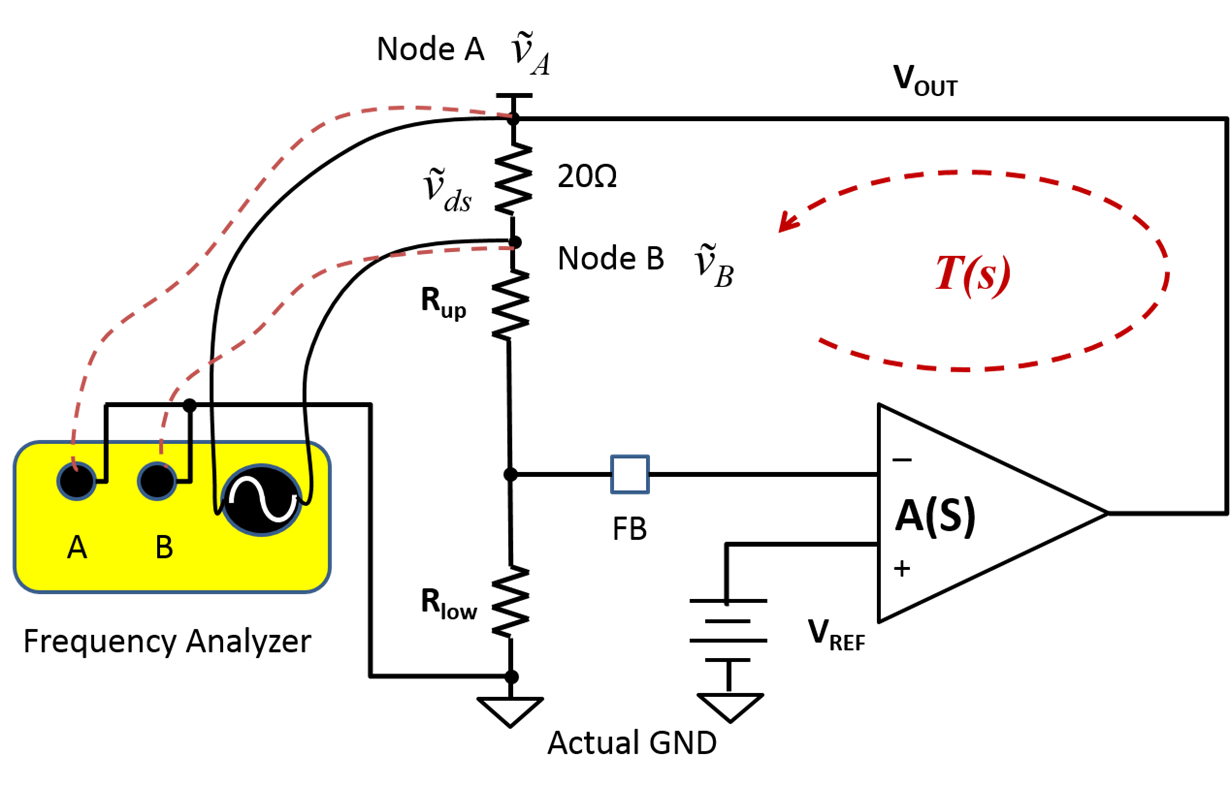
Whenever a system incorporates a negative feedback loop, the loop gain, T, becomes an important performance parameter to measure and optimize for stability, output regulation and transient-response performance. Voltage injection is a widely adopted method for measuring T. Figure 1 shows a typical voltage-injection T measurement setup. The feedback path is cut off between VOUT and Rup. A disturbance voltage is inserted. All signals refer to ground.

Figure 1: Typical T measurement setup

Equation 1 measures T as:

                           (1)                 


Signal receivers A and B have two leads which provide a reference point for signals A and B, respectively. Figure 2 shows the leads.

Figure 2: Probes of receivers A and B with their reference leads

In most cases, these leads connect to ground, and because of that, they are called GND leads. But is that always the case? To answer that question, I will demonstrate an example using the LM4041-N, a precision shunt voltage reference. Figure 3 shows a typical application circuit for the LM4041-N.

Figure 3: LM4041-N typical application circuit

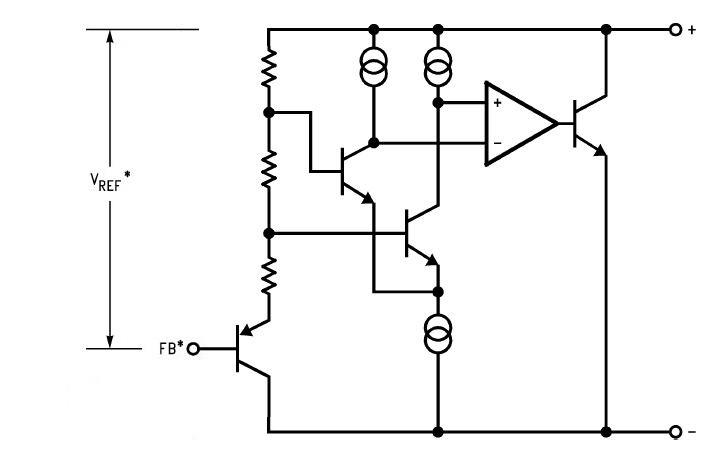
The LM4041-N keeps the voltage across VO to the FB pin at 1.24V, as Figure 4 shows. The resistor divider sets the output DC voltage. RS provides current for the LM4041-N and load.

Figure 4: LM4041-N block diagram

To generate a 2.5V reference from a 12V bus, I used these components:

  • R1 = 10kΩ.
  • R2 = 10kΩ.
  • RS = 10kΩ.
  • Co = 0.22µF.

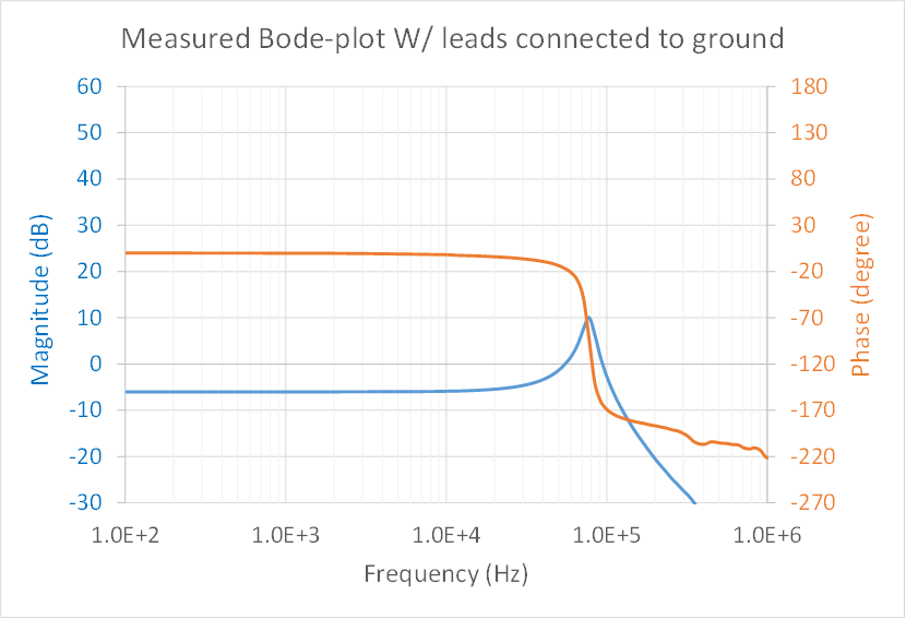
Figure 5 shows the Bode plot measurement result using the setup shown in Figure 1. The result does not correspond to tight DC regulation, as I expected. Nor does it provide a direct indication of stability.

Figure 5: Measured Bode plot with reference leads connected to ground

I derived the AC small-signal models referring to ground. Figure 6 shows the model.

Figure 6: Small-signal model referring to ground

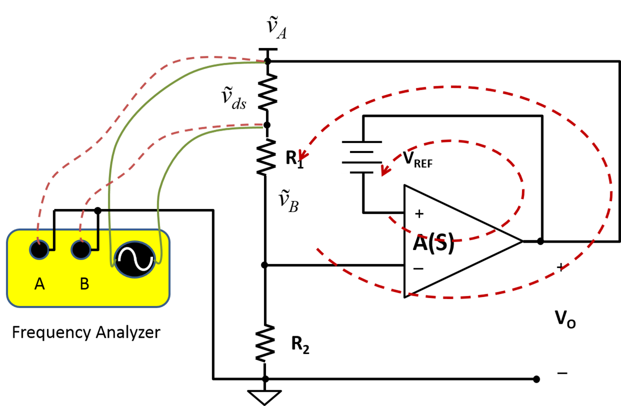
 With the reference leads connected to ground, the break point between Vo and R1 only cutting off part of the feedback path. I examined the LM4041-N block diagram. The positive input of the gain stage connects to Vo from the AC perspective. By moving the reference leads to Vo, I now can break the feedback loop completely between R2 and ground. At this break point, looking backward is the regulator output, RS and Co in parallel. R2 is the impedance looking forward. For most frequencies, the impedance of Co is much smaller than R2. Figure 7 shows the small-signal model referring to Vo.

Figure 7: Small-signal model referring to the output

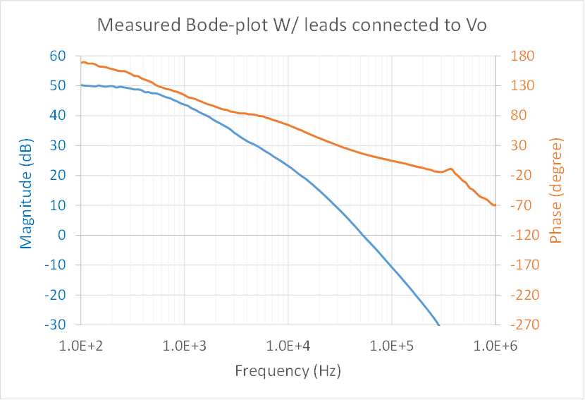
Figure 8 shows the measurement results using the setup shown in Figure 7.

Figure 8: Measured Bode plot with reference leads connected to Vo

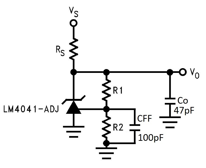
The result shown in Figure 8 indicates that the stability needs improving. I reduced the output capacitor from 0.22µF to 47nF and added a phase-boosting capacitor in parallel to R2, as shown in Figure 9.

Figure 9: Final schematic of LM4041-N as a 2.5V voltage reference

Figure 10 shows the improvement with the reduced Co and phase-boost capacitor, Cff. With the changes, phase margin has increased from 16 degree to 45 degree.


Figure 10: Measured Bode plot with a different Co and Cff

You can use the LM4041-N to show how to find a point to connect the reference leads of a frequency analyzer for Bode plot measurement. First, develop an AC small-signal model. Then, identify a reference point so you can find a break point to meet both of these requirements:

  • All feedback paths are cut off at the break point.
  • The impedance of the break point looking backward is much smaller than the impedance looking forward.

Additional resources

The pioneering work that led to the DMD

$
0
0
I started working at Texas Instruments in the late-1980s, a time after Dr. Larry Hornbeck invented the digital micromirror device (DMD) in 1987. The overall development of microelectromechanical systems (MEMS) upon which DLP ® chips are based was...(read more)

Is integrated GaN changing the conventional wisdom?

$
0
0

As a power electronics engineer, there is a saying that no success is made without the lessons learned from power devices blowing up. This seemed true during my years of experience debugging switched-mode power supplies with silicon-based MOSFETs. It is through trial and error and the study of device failures that you learn how to design a converter that works reliably.

In the early stages of gallium nitride (GaN) power FETs, failures were common. More stringent gate-loop design requirements, much higher dv/dt and the effect of common-source inductance all made the circuit much more sensitive to parasitics and noise. When TI’s first 600V GaN power stage samples came out, I marveled at the product’s robustness and the effectiveness of its self-protection functions. Even though the power stage had been validated through rigorous testing, my previous experience with silicon parts left me curious of its robustness under actual usage. More importantly, will these functions change the conventional wisdom of circuit prototyping and debugging ?

In a recent design of an interleaved converter, I used two TI half-bridge LMG3410-HB-EVM evaluation modules (EVMs) with some basic DC bus design, controlled by a UCD3138 digital pulse-width modulation (PWM) controller. When the two interleaved half bridges worked together, I saw that the PWM signal was repeatedly affected by high dv/dt (100V/ns), causing shoot-through across the FETs at 480V and triggering the integrated overcurrent protection (Figure 1).

Unlike the majority of FETs – which would fail in this situation – the LMG3410 integrated power stage enabled me to repeat the fault condition without damage, and to debug to the root cause quickly. This would have been very painstaking and possibly unsafe to do with traditional parts.

Figure 1: Self-shutdown of the power stage following a shoot-though event (blue: upper-FET PWM; yellow: lower-FET PWM; green: inductor current)

By varying the slew rate through RDRV, I found that 50V/ns or 100V/ns with single-phase operation had robust operation, while 100V/ns with two-phase operation did not. The root causes were contamination from common-mode (CM) noise and a nonoptimized layout of the controller’s peripheral circuits, resulting in a clock-synchronization mismatch across different PWM channels (Figure 2).

Figure 2: PWM out-of-sync leads to inductor current surge (blue: upper-FET PWM; yellow: lower-FET PWM; green: inductor current; red: fault-signal triggering)

TI’s ISO7831 digital signal isolator provides an adequately high CM transient immunity (CMTI) rate (>100V/ns), but the isolated power supply (which usually has much higher CM capacitance) would easily couple noise from the switching-node voltage to the control-side ground at high dv/dt (Figure 3). With multiple phases operating simultaneously, more CM noise would be injected into the control side.

Power-supply designers sometimes overlook this issue, since silicon devices and some GaN FETs with external drivers will not achieve such a high slew rate. I successfully resolved the issue by adding extra CM chokes on the upper FET’s isolated power supply and improving the decoupling loop of the digital controller, which reduced ground bouncing and noise coupling at the controller. Thanks to LMG3410’s integrated protection functions, I didn’t experience a single catastrophic failure during the whole debugging experience, despite repeated CM noise-induced faults.

Figure 3: CM capacitance across isolated power supply and digital isolator

Besides overcurrent faults, overtemperature events are common occurrences in power converters. Although an experienced engineer has good thermal design skills, keeping the device junction cool is still challenging, and there is not much margin for error. Over time, events such as fan failures or heatsink deterioration can cause catastrophic failures. Fortunately, the LMG3410 has integrated overtemperature protection, and it came to my rescue when my fan’s power supply got turned off accidentally. The thermal trip point is set at 165°C, allowing enough margin for brief temperature excursions but preventing the device from suffering permanent damage due to cooling-related system failures.

While GaN brings advantages in system efficiency, size and cooling, its high switching speed and frequency also present increasing challenges. The protection and other integrated functions of TI GaN products are changing the conventional wisdom of using discrete Si MOSFETs for us to learn about the intricacies of high-speed switching-converter designs. These products not only protect the device against permanent damage as we debug our new designs, but also improve robustness by preventing gate overstress under long-term operation, since an integrated driver design reduces gate ringing.

The world has seen tremendous scaling of electronics and improvement of system density with Moore’s law. This trend is now coming to power electronics, thanks to the development of GaN technology and the introduction of easy-to-use GaN power stages like the LMG3410 with self-protection features. 

Get to know TI’s GaN solutions.

Additional Resources:

Learn more about GaN reliability: 

What is the USB Type-C and Power Delivery minidock and what does it do?

$
0
0

Recently, you may have seen a new TI reference design using the TPS65982 and TPS65986 as a USB Type-C™ and USB Power Delivery (PD) port controller called a “minidock.” When I first heard about the design, I thought, what is this thing, how is it different than a regular dock, and how should I use it? In this post, I’ll attempt to answer these questions.

Aside from being more compact than a traditional dock, the minidock is also completely functional when bus-powered – that is, when the USB Type-C cable is connected from a laptop to the minidock but the minidock is not plugged in to the wall. This new feature may seem trivial, but take a walk around your home or office and see how many USB docks and hubs you have plugged in to the wall. I counted three in my office and five at home, and my bus-powered eight-channel USB hub can only provide power to one or two ports before needing to be tied down to a wall outlet.

Bus-powered accessories that you carry around – usually video adapters to convert from mini DisplayPort™ to HDMI or VGA – are called dongles, right? And that’s what a minidock is: think of it as a slightly large high-functioning dongle or a very small docking station.

Before I continue, I should mention that there are three USB Type-C ports on the minidock and that none of them are identical – but that’s OK because we did it on purpose. Here at TI, we are very excited that the USB Type-C connector has the potential to revolutionize the way we think about power, data and video ports for our common mobile electronics. But as with any new technology, it will generate some confusion and frustration until we understand it better. The soon-to-be-famous maxim “not all USB Type-C ports are created equal” is all too true, and you should keep this in mind when evaluating trade-offs as a designer and curbing expectations as a consumer. Randomly plugging a cable into every port could lead to dramatic disappointment.

Let’s take a look at the ideal setup for testing the intended features of the minidock to get the most out of this exciting new technology and its associated reference design.

Figure 1: Minidock with Ideal Connections to other Personal Electronics

When the minidock is enclosed in a market-ready casing with labels, it starts to make more sense. The ports that face forward are those that you need to plug in or unplug frequently to connect your laptop, USB thumb drive, mobile hard drive or headphones. The ports hidden on the back can remain connected without the minidock, such as the HDMI or mini-DisplayPort connection to your monitor, or the USB Type-C or barrel jack power supply to charge your battery. Just remember that when you need a video adapter to present to your boss in a meeting, you can pick up the minidock and run off without lugging around a clunky power supply.

Figure 2 is a block diagram of the minidock, with functional blocks repositioned based on their physical location on the printed-circuit board PCB. It is easy to see how to correctly connect (and how not to connect) the minidock: to get video and USB 2.0/3.1 data to and from a laptop, connect the minidock at the front-right USB Type-C port. To charge your laptop, plug the charger into the back USB Type-C port. Only an upstream-facing port (UFP) device such as a flash drive or mobile hard drive can plug into the front-middle USB Type-C port.

Figure 2: Revised Minidock Block Diagram Based on Physical Location of ICs

Although the reference design takes advantage of the available capabilities of the USB Type-C and USB PD standards (while showcasing the many integrated circuits ICs that TI has to offer in this market), because USB Type-C is so versatile there are limitless variations of how to design a product similar to the minidock. Those design ideas will have to wait until future blog posts because I’m late to an important meeting. I’m taking my minidock with me.

Additional resources:


Viewing all 4543 articles
Browse latest View live


<script src="https://jsc.adskeeper.com/r/s/rssing.com.1596347.js" async> </script>