Quantcast
Channel: TI E2E support forums
Viewing all 4543 articles
Browse latest View live

One to Watch: Dietmar Walther says 'learning from failures is essential'

$
0
0

In our ongoing series, ‘One to Watch,’ we profile the movers and shakers at TI who are making a difference through innovation or citizenship.

Dietmar Walther, technical engineerGerman engineer Dietmar Walther pushes boundaries every day; he doesn’t believe in setbacks or constraints.

“My motto is, ‘learning from failures is essential,’” he admits.

Finding out how things work is what inspires and drives Dietmar. This puts him in good company with decorated innovator Thomas Edison who famously said, “I have not failed. I have successfully discovered 1,000 ways to NOT make a light bulb."

Dietmar was in high school when he first saw how PCs connected using RS-232 cables would quickly pave the way for devices with wireless connectivity.

“Within five or six years, the world completely changed,” he said. “This triggered my fascination to find out how things work, which led to why I became an engineer.”

The delight that people have when they use technology drives Dietmar to continually develop his understanding of technical issues and challenges.

“Innovation is a very, very important thing,” he said. “TI is a strong driver for this. If you innovate in a very creative way, which really helps to solve certain issues in daily life, I think it correlates to good business.”

Dietmar particularly enjoys the variety and unpredictability of his work. “I honestly never know when I come to work in the morning what’s going to happen,” he said. “It never gets boring, and I learn each day.”

Cutting down on the noise

Dietmar Walther, technical engineerTechnically, Dietmar’s daily work involves layout and design analysis, as well as lab and production testing and measurement. But it is his work to advance the understanding of how external electromagnetic interference (EMI) can disturb the operation of devices that established his reputation within our company and helped lead to his election to the TI Tech Ladder as a member of the group technical staff.

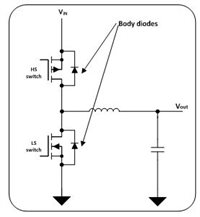
For example, think about when your radio speaker and smartphone are placed too closely together – sometimes this negatively affects operation of one or both devices – making the sound of each fade in and out and buzz or vibrate. This effect is what happens when EMI, also called radio frequency interference (RFI) or “noise” interferes.  Technically, EMI is defined as the disruption of one electronic device by another electronic device when they are in the vicinity of each other and electromagnetic fields or radio frequencies collide. 

One of the biggest achievements for Dietmar was creating a methodology to characterize the electromagnetic sensitivity of electronic devices. This methodology – Fast Transient Characterization – proved invaluable in tackling problems facing customer product design all the way down to the chip level. 

Prior to this new characterization, engineers were looking at the issue of physical damage, reset, or hang-ups from electrostatic discharge (ESD) – the sudden flow of electricity between two electrically charged objects – but only from an overall printed circuit board (PCB) inside an electronic device. However it was Dietmar who pointed out effects on the actual silicon (or chip) on the PCB during a system-level ESD strike.

“Chip designers and developers previously said they couldn’t solve application issues, but this methodology proves that chip design can be influential,” he said. “It means we’re now solving application problems that we couldn’t before.”

A large number of TI MSP microcontrollers (MCUs) benefit from Dietmar’s research. In fact, it also enabled TI customers to pass tests mandatory for electronic devices certification in Europe, helping save a lot of time and money in development.

Not only did Dietmar solve a variety of customer issues with this one technical characterization process, but he helped to make TI products more robust and more competitive. The unyielding desire to learn – not discouraged by failure —and hard work paved his way to success.

“To Dietmar, learning means doing, and vice versa,” explains Dominik Giewald, his product line manager. “He always tries to harmonize theory and practical applications and to evolve both.”

Multiplying knowledge

“With his high level of personal engagement, enthusiasm and technical leadership, Dietmar is able to learn on an individual level but to also achieve a TI-wide learning success that has a direct impact on our microchips’ resilience,” Dominik said. “To Dietmar, learning doesn’t mean only learning for himself but also sharing, so new innovation can have a broad effect and thus increase the beneficial effect for TI.”

Dietmar places strong emphasis on multiplying the knowledge he has acquired during his decade at TI. He learned a lot from more experienced colleagues and would like to pass his knowledge on to future TIers, including interns and university students whom he mentors.

“If you do not share your knowledge, people have to learn things the hard way,” he says. “You may find 1,000 ways to not invent the lightbulb, but sharing your discovery with others and the path that brought you there will keep them from doing the same 1,000 futile attempts.” 


Build a sub-20W CISPR25 Class 5 power design for automotive infotainment processors

$
0
0

In a world of always-on experiences, drivers and passengers are looking to access real-time information about traffic conditions and potential hazards via traditional radio or human machine interface (HMI) systems.  At the same time, drivers and passengers want to use connected devices like GPSs, smartphones and tablets without interference.  Thus, it is important that these devices are not affected by electromagnetic interference (EMI), which occurs when placing a large amount of electrical and electronic systems in a confined space.

EMI compliance is an important topic for many major automotive manufacturers trying to build the newest systems for cars. Requirements are stringent and manufacturers must comply with standards like CISPR 25 Class 5 and in many cases if the standard is not met, then the system cannot be sold.

The level of EMI measurement in a system is subject to an engineer’s attention mostly in the later stages of design and validation. In many cases, the engineer discovers EMI problems when the board is assembled, after all components are chosen and validated separately. At this point it is very difficult to identify the exact source of EMI since the number of switching regulators has grown exponentially in today’s advanced automotive systems. For this reason, EMI test results utilizing a reference design board is useful for the engineer to get firsthand knowledge how the different parts work with each other once assembled together on the PCB board.   

To guard against EMI problems later in the design of an automotive infotainment system for example, TI has developed the 17W System-Level Power Reference Design for Automotive Infotainment Processor Power.  This off-battery system is optimized to withstand Comité International Spécial des Perturbations Radioélectriques (CISPR) 25 Class 5 EMI limits for powering automotive processors used in infotainment and cluster systems. The typical power architecture for an automotive infotainment processor is shown in Figure 1.

There are four major blocks in the reference design:

  • The LM74610-Q1 smart diode has built in, front-end protection to withstand positive and negative pulses (International Organization for Standardization [ISO] 7630), reverse battery protection, a battery disconnect switch and overvoltage protection (OVP).
  • A common-mode and differential filter suppresses conducted EMI.
  • The LM53635-Q1 2.1MHz, fully synchronous, 3.5A DC/DC converter converts the battery voltage to a 5V rail. This device is available in an automotive-qualified flip-chip on-lead (FCOL) package with wettable flanks to minimize switch-node ringing. This DC/DC converter has low EMI characteristics using a spread-spectrum option.
  • Downstream point-of-load (POL) buck converters, such as TI’s TPS57112-Q1, TPS57114-Q1 and LM26420-Q1, provide low input voltage rails for processing power. Ferrite beads are used to remove high frequency noise on downstream power rails.

Figure 1: Typical power architecture for an automotive infotainment processor

The reference design has been tested and successfully passed CISPR 25 Class 5 conducted EMI limits.

Figure 2 shows test results for up to 30MHz of conducted emissions – peak and average detection – using all of the DC/DC switching regulators with a full load.


Figure 2: Conducted EMI results with frequency range below 30MHz

Figure 3 shows the test results for 30MHz to 108MHz of conducted emissions with the same conditions.

Figure 3: Conducted EMI results with frequency range between 30MHz and 108MHz

A reference design is a useful tool for an engineer to review EMI results and identify possible interference problems early in the design cycle. Measuring conducted EMI on a reference design board can help to identify noise trends and early compliance issues that might not appear until the final product design. Download the 17W System-Level Power Reference Design for Automotive Infotainment Processor Power reference design or get more information on TI’s power products for automotive applications.

Buck-boost regulator benefits automotive conducted immunity

$
0
0

An automotive battery’s steady-state voltage ranges from 9V to 16V depending on its state of charge, ambient temperature and alternator operating condition. However, the battery power bus is also subject to a wide range of dynamic disturbances, including start-stop, cold crank and load-dump transients.

Each automotive manufacturer has a unique and extensive conducted immunity test suite in addition to the standardized pulse waveforms given by industry standards such as International Organization for Standardization (ISO) 7637 and ISO 16750. Table 1 identifies several undervoltage and overvoltage automotive transient profiles.

 Table 1: Automotive battery continuous and transient conducted disturbances with related test levels

 Alternator-induced noise

One particularly troublesome source of noise within the audio frequency range is an automotive alternator causing a residual alternating current on its output, leading to alternator “whine” and supply modulation issues. ISO 16750-2 section 4.4, mentioned in Table 1, describes a ripple voltage on the alternator’s output in the frequency range of 50Hz to 25kHz, with a peak-to-peak amplitude (VPP) of 1V, 2V and 4V depending on the test pulse severity level. See Figure 1.

 Figure 1: An ISO 16750-2 superimposed alternating voltage test (a); a log frequency sweep profile from 50Hz to 25kHz over a two-minute sweep duration (b)

In many vehicles, a centralized passive-circuit-protection network consisting of a low-pass inductor-capacitor (LC) filter and transient voltage suppressor (TVS) diode is used as a first line of defense for transient disturbance rejection. Automotive electronics located downstream from the protection network are then rated to survive transients up to 40V without damage. However, the required cutoff frequency of the LC filter to attenuate low-frequency disturbances makes the filter inductor and electrolytic capacitor quite large. What’s required is an active power stage that eliminates the bulky passive filter components and provides a compact and cost-effective solution for tight voltage regulation and transient rejection.

Four-switch synchronous buck-boost regulator

The benefit of a wide VIN buck-boost regulator solution lies in its high power-supply rejection ratio (PSRR), offering excellent transient dynamics to attenuate input voltage transients. With that in mind, I recently wrote an article, “Automotive front-end buck-boost regulator actively filters voltage disturbances,” that describes a high density solution for automotive applications.

Figure 2 shows the schematic of a four-switch buck-boost regulator designed to output a tightly regulated 12V rail. This solution is ideal for critical automotive functions including drive trains, fuel systems, and body and safety subsystems where loads must remain powered without glitches during even the most severe battery-voltage transients. This easy-to-use design tool streamlines regulator design and implementation for faster design-in and time to market.

Figure 2: Four-switch synchronous buck-boost solution with a wide VIN range of 3V to 36V

Figure 3a shows the buck-boost regulator’s output voltage waveform when a DC input of 9V has a superimposed sinusoidal ripple with a peak-to-peak amplitude of 1V and a frequency of 1kHz. The input ripple is attenuated by approximately 40dB. Figure 3b shows the output voltage during a cold-crank transient down to 3V for 20ms using an automotive cold-crank simulator. The four-switch buck-boost converter regulates seamlessly through the cold-crank profile.


Figure 3: Measured four-switch buck-boost converter: ripple rejection at a 9V DC input (a); cold-crank performance (b)

Summary

With its high PSRR, high efficiency and low overall bill-of-materials cost, a four-switch synchronous buck-boost like TI’s LM5175-Q1 current-mode controller offers a useful solution for mitigating transient disturbances in automotive applications. This buck-boost controller is automotive qualified to facilitate its integration into vehicular 12V single-battery and 24V dual-battery systems.

Additional resources:

Waveform audit: rabbit ears

$
0
0

What does an interning doctor diagnose if he sees symptoms he has never read about in a medical handbook? A similar question can be asked of an integrated circuit (IC) validation engineer early in his career. Indeed, like a doctor, a validation engineer is assigned to evaluate the “state of health” of an IC and to make the correct “diagnosis,” which sometimes requires a deep understanding of the device “anatomy,” combined with practical experience.

A physician may begin an examination by monitoring the patient’s heartbeat. A validation engineer of a switched-mode DC/DC converter also monitors heartbeats: the switching node. But what if the switching waveform does not look like what most textbooks show? Does that indicate some kind of device “disease,” or can the engineer interpret the state as normal?

Another Waveform Audit blog "My boost converter has an off-ramp!" already explained one surprising behavior of a switching node, so in this post I will talk about “rabbit ears” – a “symptom” occurring as small bumps during switch-node toggling.

Consider a synchronous buck converter (Figure 1) operating in continuous conduction mode. At t1 (Figure 2), the low-side switch turns off and the high-side switch turns on. From t1 to t2, the high-side switch is on and Vsw is equal to VIN (neglecting RDS(on) losses). During this time, the inductor current is increasing. At t2, the high-side switch turns off, the low-side switch turns on and the inductor current starts to flow through it. From t2 to t3, the low-side switch is on, Vsw is equal to GND (neglecting RDS(on) losses). During this time, the inductor current is decreasing. At t3, the cycle starts again.

You can find typical waveform diagrams of the switching pin and inductor current shown in Figure 2 in most literature. If you go to the lab and take measurements, however, you will see that the oscilloscope picture (Figure 3) can look a bit different – it can show “rabbit ears” on the switching node at switching moments. What causes this?

Figure 1: Simplified diagram of a synchronous buck converter


Figure 2: Waveform diagrams of the inductor current (IL) and the switching node (Vsw) of a buck converter operating in continuous conduction mode


Figure 3: Oscilloscope picture of the inductor current and switching node with rabbit ears

The secret is that the simple model shown in Figure 2 does not take into account the switching dynamics. In reality, the transition between switching phases is not instantaneous. Several nanoseconds are required to turn the transistors of the output stage on and off. To avoid cross-conduction between the switches, one should open before another starts to close. The time when both transistors are off (open) is called “dead time.”

Where does the current flow when both switches are off? In fact, metal-oxide semiconductor field-effect transistors (MOSFETs) have a parasitic body diode between the drain and the source (Figure 4), so during dead time the inductor current flows through the body diode of one of the switches. Within this time, the amplitude of the switching node increases by a value approximately equal to the diode’s forward voltage drop. This increase in amplitude shows up in the switch-node waveform as a rabbit ear.

Figure 4: Simplified diagram of the output stage and output filter of a synchronous buck converter

The position of rabbit ears depends on the direction of inductor current at the moment of switching. In most applications, a buck converter sources the current. But there are applications where a buck converter should be able to sink current as well. For example, the TPS65175, a fully programmable liquid crystal display (LCD) bias IC, integrates an HVDD buck converter that can both sink and source current.

Table 1 summarizes five cases of different positions of rabbit ears for synchronous buck converters.

Table 1: Different positions of rabbit ears for the synchronous buck converter depending on the inductor current direction  


Figure 5: Conduction of the high-side body diode (a); conduction of the low-side body diode (b)

If switching nodes were heartbeats and validation engineers were physicians, they would diagnose the presence of rabbit ears as normal. Rabbit ears do lead to a slight efficiency reduction, as some energy is lost during body diode conduction. The challenge then becomes how to optimize the switching time for switched-mode DC/DC converters.

One last thing – do not mix up rabbit ears with the ringing effect described in the Analog Applications Journal article, “Controlling switch-node ringing in synchronous buck converters,” or with the switching spikes caused by bad probe techniques.

Additional resources:


How to balance efficiency and settling time with highly integrated DACs

$
0
0

In my first post, I talked about the need for modular, flexible and smart design in analog output modules and explored methods for improving efficiency in a typical high-side voltage-to-current converter used to drive 4-20mA outputs. Figure 1 shows an implementation that involves a buck/boost converter in a simple feedback network to supply just the necessary power to the load. While this implementation makes 4-20mA generation highly efficient and thermally optimized, it comes with a reduced settling time. So in this post, I will explore how to balance efficiency without sacrificing settling time.

Figure 1: High-side voltage-to-current converter with a buck/boost converter

As an example, let’s assume a load of 1kΩ. If the digital-to-analog converter (DAC) code changes from a 4mA output to a full-scale 24mA output, the buck/boost converter will boost from approximately 7V to 27V, as the system is fully adaptive. Since the buck/boost converter needs to charge the large storage capacitor, the settling time of the system could be as large as a couple of milliseconds, as shown in Figure 2. In such a fully adaptive system, the settling time is completely dominated by the buck/boost converter. However, some systems need to have a relatively faster settling time while still meeting efficiency requirements.

Figure 2: Settling time for a fully adaptive system

You can meet this goal using TI’s DAC8775, a quad-channel 16-bit 4-20mA DAC with adaptive power management. This DAC integrates an analog-to-digital converter (ADC) to sense the load and set the buck/boost converter to a fixed value.

The block labeled “Auto Learn” in Figure 3 is a high-level representation of this system. Based on the ADC’s calculation, the buck/boost converter clamps to a fixed value, which satisfies compliance for a full-scale output current at a given load. Once the DAC code written exceeds quarter scale, auto-learn mode kicks in, starts calculating the load in the background, and sends the information to the buck/boost converter to adjust its value. This results in the buck/boost converter clamping the supply to the value needed to support the maximum current for the given load. The settling time of the system then becomes dominated by the DAC which is typically more than an order of magnitude faster than the buck/boost settling. 

Figure 3: The DAC8775’s integrated ADC senses the load

Back to our example 1kΩ load: once enabled, auto learn will calculate the load as 1kΩ and set the buck/boost converter to 27V. This achieves the maximum power saving without sacrificing settling time. As you can see in Figure 4, after the buck/boost output settles, all of the consecutive DAC code updates settle within 10µs. This is a significant improvement in settling time.

Figure 4: Setting time with auto-learn mode


Another advantage of such an implementation is that it makes modules more flexible. System designers don’t need to spend engineering time to optimize modules for different loads. This implementation enables the system to “learn” the load automatically and adjust the configuration as necessary. In addition, because auto-learn mode runs in the background, it saves costs during installation.

We will continue to cover topics around trends in factory automation in subsequent blogs. Until then, learn more by checking out TI’s broad precision DAC portfolio or the DAC8775.To get posts like this delivered to your inbox, sign in and subscribe to Precision Hub.

Additional resources

How to build a wireless controller

$
0
0
Digital Systems Teaching and Research (DSTR) Robot Controller Tutorial Students at Texas A&M University have developed the DSTR Robot – a small form factor robotic platform – in the University’s Mobile Integrated Solutions Laboratory...(read more)

Increasing battery life in IoT devices

$
0
0
Wireless sensors are gaining popularity with the installation of more smart devices in homes and buildings. Battery-powered wireless devices enable very easy installation almost anywhere, but changing batteries frequently is not ideal from an ease-of...(read more)

The secret to moving faster with Bluetooth® 5

$
0
0

As the speed increases with Bluetooth® 5, don’t you want to move quickly too? Now it’s easy to pick up the pace with the first fully qualified Bluetooth 5 protocol stack for single-mode Bluetooth low energy applications from TI, supporting high-speed mode.

Bluetooth 5 is groundbreaking. The new high-speed mode allows data transfers up to 2Mbps, twice the speed of Bluetooth 4.2 and five times the speed of Bluetooth 4.0, without increasing power consumption. And in addition to faster speeds, this mode offers significant improvements for energy efficiency and wireless coexistence with reduced radio communication time. Lastly, Bluetooth 5 enables unparalleled flexibility for you to adjust speed and range based on application needs, capitalizing on the high-speed or long-range modes respectively.

Because data transfers are now possible at 2Mbps, you can develop applications using voice, audio, imaging, and data logging that were not previously an option using Bluetooth low energy. With high-speed mode, existing applications will deliver faster responses, richer engagement and longer battery life. Not to mention, Bluetooth 5 enables faster, reliable firmware updates.

The SimpleLink™ Bluetooth low energy CC2640R2F wireless microcontroller (MCU)– which is already in mass production – is the tiniest Bluetooth 5 solution (see Figure 1) with fierce radio-frequency (RF) performance optimized for Internet of Things (IoT) end nodes. The CC2640R2F device is also ideal for industrial applications since it can be easily added to an existing host MCU as a network processor to ensure system design flexibility.

Figure 1: Package sizes for the CC2640R2F wireless MCU

Developers interested in trying out the extended range can also test drive the Bluetooth 5 coded physical layers (PHYs) (the long-range mode) using two CC2640R2F LaunchPad™ development kits (kit shown in Figure 2) to measure the achievable distance of this mode.

Figure 2:CC2640R2F LaunchPad development kit

The real secret to moving faster with Bluetooth 5 is getting started today. Whether you are designing a connected medical device, smart meter or motor condition monitor, Bluetooth 5 enables you to double your speed. With TI’s fully qualified Bluetooth 5 protocol stack, you can rapidly start development today and have more time to innovate.

Get started by downloading the industry’s first fully qualified Bluetooth 5 protocol stack (BLE5-Stack)!

Additional resources:


Smart sensing with ultra-low-power MCUs – part 4: Holter monitor

$
0
0
In the fourth installment of this six-part smart sensing series , I would like to discuss the operating principle and implementation of the Holter monitor. An electrocardiogram (ECG) graphically records the electrical activity of the heart and recognized...(read more)

Achieving higher-accuracy battery fuel-gauge performance in ultra-low-power systems

$
0
0
Whether designing ultra-low-power portable handheld devices or remote wireless battery-powered sensor nodes, the need to accurately measure, predict and report battery state-of-charge, battery health and remaining device operating time is becoming increasingly...(read more)

Is PMBus still useful without telemetry?

$
0
0

PMBus is an Inter-Integrated Circuit (I2C)-based communication standard/interface for power-supply management. Many point-of-load (POL) converters on the market today are built with the PMBus interface, which enables digital communication between converters and their hosts. The host can be any microcontroller, microprocessor, computer, board-management controller, automatic test equipment or application-specific integrated circuit/field-programmable gate array. There are four general types of communication between the converter and host: command, control, sequence and monitor. A PMBus device can support any combinations of the above communication types.

To know which PMBus device to choose for a particular application depends on the application environment and price point. Generally, PMBus devices designed to provide monitoring functions such as input voltage, input current, output voltage, output current and die temperature have significantly higher silicon and design costs because of the addition of a precision analog-to-digital converter circuit design.

The monitoring capability through PMBus is generally referred to as “telemetry.” Figure 1 shows a graphical user interface (GUI) generated by TI’s Fusion Digital Power™ designer software. The GUI displays three telemetries: output voltage, output current and temperature.

Telemetry is also very useful in systems where data analysis and system characterization are essential. In high-reliability systems where live performance monitoring and failure analysis are absolute musts, the right kind of telemetry can provide great value.

Figure 1: TI Fusion Digital Power GUI for live telemetry reading

Even though telemetry is a very useful feature in a PMBus device, not every system or application has the right environment or the need to take advantage of the feature, especially since PMBus devices with telemetry normally cost more than devices without telemetry. But the value and benefit of PMBus is so compelling that even without telemetry, it is still worth your consideration.

One of the major benefits of PMBus is the cost savings that it brings to the overall system bill of materials (BOM). Integrating the PMBus interface into the POL converter eliminates external pin-strapping components that analog designs need to program converter configurations such as switching frequency, current limit, under voltage lockout, soft-start time, power good delay and voltage margining/tracking components.

Figure 2 shows the waveform of adaptive voltage scaling behavior by using the TPS549D22, a 40A PMBus synchronous step-down converter. A voltage identification digital (VID) chip like the TI LM10011– with several resistors to support the identical voltage scaling functionalities – is necessary to support the series of digital events shown in Figure 2. The PMBus benefit includes not only BOM cost optimization, but also the printed circuit board area reduction achieved by fewer components and routing traces.

Figure 2: TPS549D22 digital events driven by a 1MHz PMBus device

TI offers several unique high performance and high current converter families. Figure 3 summarizes TI’s PMBus and multi-chip module (MCM) converter products, including the TPS549D22, which is the highest current rated (40A) synchronous buck converter with PMBus, albeit without telemetry. Figure 4 shows the detailed PMBus command sets for the TPS549D22

Figure 3: PMBus converter selection at a glance


Figure 4: Total PMBus command sets supported by the TPS549D22

Today, PMBus is widely adopted as an effective communication means between the load and its power supply source during design, production test and every day in-system usage. Choosing the right PMBus feature for the power supply application becomes increasingly critical due to multiple considerations contributing to the success of the overall design, including functionality, performance and cost. PMBus without telemetry is still useful when it comes to configuring and controlling all the power sources, and the high integration simplifies design.

For more information on designing with PMBus, read the Power House blogs “PMBus benefits in multi-rail systems,” and “Save PCB space and overcome point-of-load design complexity with PMBus modules.”


What floats your boat? Exploring linear regulators in medical ultrasound

$
0
0
Let’s say that you are working on an ultrasound system . You require a clean ±100V supply to power the ultrasound transmitter, so you need a linear regulator (LDO). How do you tackle this requirement? You could look for a device from...(read more)

Bringing new intelligence to industrial applications with mmWave sensors

$
0
0
From position and proximity to level and light, sensing solutions provide a means to sense, digitize and process the world around us. Application-specific problems have given rise to a multitude of different sensing technologies that enable systems to...(read more)

Giving cars advanced vision through TI mmWave sensors

$
0
0

Advanced driver assistance systems (ADAS) have rapidly evolved over the last five years, from comfort functions, such as adaptive cruise control (ACC), to safety-enhancing functions such as emergency braking and newer applications like pedestrian detection and 360-degree sensing.  Previous millimeter wave (mmWave) sensors which enabled these applications were all discrete, with the transmitters, receivers and the processing components as separate units. This made the design process of the mmWave sensor complex and the solution big and bulky.

By bucking the trend of traditional silicon germanium- (SiGe) based sensor technology, TI’s RFCMOS-based radar sensors bring in a high level of digital and analog integration to enable high output power, low power consumption (50 percent less compared to existing solutions in market) and low-phase noise, in turn resulting in accurate and ultra-high resolution sensing enabling a safer and advanced driving experience.

With three devices in TI’s mmWave sensors portfolio, AWR1243, AWR1443 and AWR1642 sensors, developers can choose the right range and level of sensitivity for their design needs.  

The AWR1x sensors work on frequency modulated continuous waveform (FMCW) technique in the 76 – 81 GHz band and have the following features:

  • Closedloop phase locked loop (PLL) enables linear and highly precise chirps which helps with increased range accuracy.
  • Ability to sweep the complete 4 GHz chirp bandwidth, which enables detection of objects spaced less than 5 cm apart.
  • A complex receiver architecture that enables jamming or interference detection in a dense sensor environment.
  • An intelligent self-monitoring system that self-calibrates across voltages and temperatures.

Long- and mid-range sensing applications

Imagine driving at a high speed on a highway with automatic cruise control. If any obstacles were to appear in the vicinity of your car at a certain distance or curvature, the mmWave sensor can help detect this obstacle in a matter of milliseconds (ms). The central intelligent system will then alert the driver within 100 ms to take the necessary action to help alert the driver of possible danger.

The AWR1243 mmWave device, as displayed in Figure 1, is a radar front-end sensor with three transmitter and four receiver antennas targeted toward long and mid-range radar applications like ACC and automatic emergency braking (AEB) which are required for autonomous driving. It comes with the camera serial interface-2 (CSI-2)/low-voltage differential signaling (LVDS), I2C and serial peripheral interface (SPI). The monolithic mmWave integrated circuit (MMIC) comes with an inbuilt calibration and monitoring engine and is coupled with an external processor such as the TI TDA3 processor. Cascading multiple AWR1243 sensors can easily achieve farther range and better angular resolution in an application such as imaging radar for automated highway driving.

Figure 1: AWR1243 mmWave transceiver, the range and field of view capability

Short-range applications

According to the Eno Center for Transportation, about 90 percent of car accidents are due to human error; many of the accidents caused by driver distraction. Cameras, 24 GHz radar and ultrasonic sensors exist on the market to help address these problems, but the products may not be the best fit.  This is where TI’s 77 GHz single-chip digital signal processor (DSP) integrated solution can make a difference. Our mmWave sensors can work under any environmental condition like day, night, snow, rain, fog and dust and provide highly accurate measurements in a small form factor with low-power consumption.

The TI AWR1642 sensor offers the below features compared to a 24 GHz sensor:

  • 33 percent smaller form factor
  • 50 percent less power consumption
  • 10x more range accuracy
  • Cost-optimized bill of materials (BOM)

The AWR1642 is a high-end, single-chip mmWave sensor, as show in Figure 2, with two transmitter and four receiver antennas targeted toward short-range and ultra-short-range applications like blind-spot detection, lane-change assistance, cross-traffic alert and stop and go. It comes with CAN, CAN flexible data rate (CAN FD) and SPI interfaces, as well as 1.5 MB of on-chip RAM. An ARM® Cortex®-R4F and TI C674x DSP handle data processing

The presence of a hardware-in-loop (HIL) interface enables feeding of raw analog-to-digital converter (ADC) data collected in the field back to the sensor, which enables the analysis of the data path and algorithmic development. A crypto accelerator encrypts object/raw data sent to the engine control unit (ECU) through the CAN/CAN FD interface.

The ARM Cortex-R4F can run automotive open systems architecture (AUTOSAR), clustering and tracking algorithms. For signal processing-intensive applications like Fast Fourier Transform (FFT) and object detection, the C674x DSP can perform both fixed- and floating-point operations.

Figure 2: AWR1642 single chip sensor and its range, field of view capability

Ultra-short range applications
Proximity sensing applications, such as parking assistance, occupancy detection, car door/trunk openers and simple gesture movements, are becoming important implementations in current and future vehicle designs.

The AWR1443 is a 77 to 81 GHz highly integrated radar device that can be used in such applications. The AWR1443 device, show in Figure 3 below, includes the entire mmWave RF and analog-based band signal chain for three transmitters and four receivers, as well as a customer programmable ARM Cortex R4F with 0.5 MB of on-chip memory to enable autonomous operation of the front end.
 
Figure 3: AWR1443 single chip sensor 
Get started today
To get started developing your radar solution, TI provides evaluation modules (EVM) for all the three devices (AWR1243,AWR1443, AWR1642), reference schematics, layout and BOM which will enable you to build your own board in a short time.
Additionally, TI provides mmWaveSDK, a software development kit which comprises of device drivers, an operating system (OS) abstraction layer, libraries of reference algorithms, firmware, APIs, utilities and demo examples. The libraries facilitate control and monitoring of RF front-end subsystems, while the drivers provide external communications through standard peripherals. The mmWaveStudio tool helps the developer to configure the RF front end at the system level parameters like chirp and profile configurations, start and end frequencies and much more and analyze the RF performance.

By leveraging TI’s software and system development kit (SDK) developers can evaluate and enable a sensor project in less than 30 minutes.

Learn more about the most precise mmWave sensor on the market today:

New mmWave sensors offer unprecedented accuracy for automotive, industrial applications

$
0
0

New mmWave sensors offer unprecedented precision for automotive, industrial applications

The world is changing. You can see it on the roads, in buildings and in cities.

Meeting that change is a new family of highly accurate, single-chip millimeter-wave (mmWave) sensors enabling applications ranging from automotive radar to industrial automation. These precision sensors give designers a platform to bring new levels of intelligence, safety and autonomy to automobiles, buildings, factories and drones. Advances in technologies such as mmWave sensors are timely. For example:

These changes will require new levels of precise sensing to detect the range, velocity and angle of objects; to penetrate plastic, drywall, glass and other materials; and perform in extreme and challenging environmental conditions such as rain, fog, dust, light and darkness.

Until now, sensing systems have used discrete components to transmit, receive and analyze signals. Using discrete components on circuit boards increases the size, power and overall cost of systems. Our technology − built on a complementary metal-oxide semiconductor (CMOS) platform − integrates a best-in-class digital signal processor (DSP) and microcontroller (MCU) into a single, small package that will use less power while delivering up to three times more accuracy than current solutions.

Automotive applications

New mmWave sensors offer unprecedented precision for automotive, industrial applicationsSensors in automotive applications will support advanced driver assistance systems (ADAS) designed to help warn, brake, monitor and steer our cars as we drive to the grocery store, to work and on long road trips across the country. These increasingly in-demand systems are essentially the first step on the technology road toward full autonomous driving.

Technologies widely available in cars today include adaptive cruise control, automatic emergency braking, blind-spot warning, lane-departure warning and even parking assistance. But future advances – autonomous parking, highly automated driving and, ultimately, hands-off-the-wheel autonomous driving – will depend on increasingly sophisticated sensing intelligence from radar, as well as from technologies such as laser, ultrasonic, infrared and lidar.

Industrial applications

These sensors are enabling the next level of efficiency and intelligence for buildings and factories.

The applications for industrial systems are myriad. For example, the sensors’ unprecedented accuracy will enable companies to precisely measure the fluid levels in tanks as a way to manage inventory and detect leaks early. Perimeter sensors will provide security systems with precise motion-sensitive detection and tracking. Traffic-monitoring systems enabled with mmWave sensors will create smarter cities through reduced traffic stress.

Sensors also will provide more precision for robots and forklifts and be able to determine how many people are in a room.

Our world is in the midst the next great industrial revolution that will require unprecedented precision. Technologies such as mmWave will enable designers to meet these needs in new, innovative ways. 


Miniaturization of mmWave sensors enabled by CMOS technology

$
0
0

Most commercial radar systems, specifically those in advanced driver assistance systems (ADAS), are based on silicon-germanium (SiGe) technology. Today’s high-end vehicles feature a multichip SiGe radar system. While SiGe radar systems meet the high speeds demanded by 77GHz automotive radar for adaptive cruise control, they are big and bulky, taking up a lot of board space.

As the number of radar sensors in vehicles climbs to at least ten (front, rear and corners), space constraints dictate that each sensor be smaller, lower power and more cost-effective. Some current radar systems under development will push the integration of the transmitter, receiver, clock and baseband functionality into a single chip, which will reduce the number of front-end chips from four to one. But that is just for the radar front end.

TI has taken integration to the next level, leveraging complementary metal-oxide semiconductor (CMOS) technology to integrate intelligent radar front ends with embedded microcontrollers (MCUs) and digital signal processing (DSP) capabilities. Processing is co-located with the front end to minimize radar system size, power, form factor and cost, further enabling the mounting of multiple radar systems in vehicles.

Figure 1: Single chip integration enabled by CMOS

Classical advantages of CMOS technology include higher transistor density and lower power. Digital scaling in CMOS decreases the power and size and increases performance at every node. Driven by these digital transistor improvements, the speed of CMOS continues to increase and is now sufficient for 79GHz ADAS applications. The 79GHz band offers the 4GHz bandwidth essential for higher-range resolution. Future radar systems will also need support for short range, with better angular resolution translating to more antennas in the radar systems. TI’s sensors in CMOS technology can support this scalability to high-volume mass production.

CMOS technology has further enabled TI to embed the digital within the analog, leading to new system configurations and topologies for radar system deployment. For example, embedded MCUs in TI’s single-chip millimeter-wave (mmWave) sensor enable semiautonomous control of radio frequency (RF) and analog subsystems. TI’s CMOS sensors provide digital assistance to the analog, for adaptation, flexibility and robustness over environmental and manufacturing variations. Digital assistance extends to real-time control of flexible chirp generation and advanced self-monitoring capabilities.

The dynamic range of a radar system depends on receiver noise floor and tolerances to self-jamming caused by bumper reflection. These heavily depend on architecture and system capabilities such that a CMOS system – with wider intermediate frequency (IF) bandwidths, more channels and precise low-noise linear closed-loop chirp generation – can have superior system-level performance for certain radar applications.

CMOS technology changes the design of mmWave sensors, embedding increased intelligence and capabilities. CMOS technology has enabled TI to deliver a high-performance, low-power mmWave sensor portfolio, scaling from a high-performance radar front end to single-chip radar.

Additional resources

SimpleLink™ MCU SDKs: RTOS and POSIX

$
0
0

Welcome to the second installment in a series of blog posts that will review the major components of the SimpleLink™ microcontroller (MCU) platform’s software development kits (SDKs). These SDKs feature common components and device-specific middleware that speed time to market and provide a unified development experience across the entire SimpleLink MCU portfolio of wired and wireless devices. Refer to Figure 1 below for a block diagram of the SimpleLink SDK. In this post, I will dive deeper into how components included within the SimpleLink SDK enable you to create deterministic, efficient, scalable applications with a real-time operating system (RTOS).

Figure 1: SimpleLink SDK

TI-RTOS
The SimpleLink SDK is integrated with TI-RTOS, a full-featured real-time OS. All TI SimpleLink SDKs come with the TI-RTOS kernel pre-installed and are Portable Operating System Interface (POSIX)-compliant. TI-RTOS is a robust solution you can trust, already deployed in thousands of applications across various TI embedded solutions. The kernel is open source (Berkeley Software Distribution [BSD] license) and was developed in lockstep with TI’s silicon portfolio to enable very low latency in an efficient code footprint. TI-RTOS helps you optimize your applications for power consumption, performance and code size to meet your unique needs. Specifically, TI-RTOS’ power-management capabilities enable you to achieve aggressive power savings for your applications with minimal effort and intuitive application programming interfaces (APIs).

At the center of the TI-RTOS kernel is the scheduler, which ensures that the highest priority thread is running. This offers deterministic and fast operation. TI-RTOS supports four different types of threads: hardware interrupts (Hwis), Software interrupts (Swis), task and idle, shown in figure 2 below. TI-RTOS offers several thread-communication mechanisms such as semaphores, mailboxes, queues, gates and events. Furthermore, TI-RTOS includes system-level timing services and memory managers to ensure that your application is as efficient and lean as possible.

Figure 2: Types of threads supported in TI-RTOS

FreeRTOS
The SimpleLink SDK was developed to be modular, allowing you to use alternative RTOS kernels beyond TI-RTOS. In addition to TI-RTOS, the MSP432™ and Wi-Fi® CC3220 software development kits (SDKs) also include the ability to use the popular FreeRTOS. The modularity of SimpleLink SDKs make it easy for you to plug in your OS/kernel of preference for maximum flexibility.

POSIX
The SimpleLink SDK also offers POSIX-compatible APIs. POSIX is an Institute of Electrical and Electronics Engineers (IEEE) industry API standard for OS compatibility. The POSIX layer abstracts the RTOS kernel functionality used by applications. Requiring less than 2KB of code in typical applications, the POSIX layer enables the reuse and porting of examples and user applications to a different kernel. Using this layer is optional, but it means that you can use whatever OS you are currently familiar with or want to move to in the future. POSIX compatibility also allows TI third-party partners to interface with SimpleLink SDK devices to add support for their kernel, providing complete freedom to design with any OS, including FreeRTOS.

Runtime Object Viewer
To help you optimize your RTOS-enabled application, TI offers powerful tools to help you debug and monitor your code. Specifically, the Runtime Object Viewer (ROV2) offers a powerful visualization and instrumentation interface to help you monitor thread states, heap usage and central processing unit (CPU) load. Figure 3 below shows a few available dashboards to help you debug. While the ROV2 can provide helpful insight into your RTOS-enabled application, the ROV2 tool is flexible enough to display high-level information relevant to any library, RTOS or not, within your application.

Figure 3: Views available in Runtime Object Viewer utility

Explore more
To learn more about the SimpleLink MCU SDK, review the white paper, “Simplifying software development to maximize return on investment,” visit SimpleLink Academy or download the SDK and start coding immediately with CCS Cloud.

The next installment of this SimpleLink MCU SDK series will provide more insights on Bluetooth® low energy stacks.

Lightning-fast internally-compensated ACM topology – what can it do for you?

$
0
0

Internally compensated advanced current mode (ACM) is a new control topology from Texas Instruments that supports true fixed-frequency modulation and synchronization with internal compensation. Fundamentally, it is similar to emulated peak-current-mode (PCM) control, which maintains stability over a range of input and output voltages for fast transient response. What makes ACM different is that it is a ramp based, peak current mode control scheme that internally generates a ramp to achieve true fixed frequency, without using external compensation.  As well, ACM has good immunity for power-stage (inductor and capacitor) variation, but I will go into more details on the virtues of ACM here.

Why internally compensated ACM?

There are control topologies that support either true fixed frequency or pseudo fixed frequency without the need for an external compensation network. However, there are some drawbacks to using these.

Most existing true-fixed-frequency/no external compensation converters are based on traditional peak current mode, which moves the compensator from outside the package to inside the circuitry, with the internal compensator designed and optimized to cover a variety of applications. Because the internal compensation needs to cover a variety of stability ranges, the internal loop and slope compensation are very difficult to optimize if you need to achieve a fast transient response. The loop bandwidth must also be limited to accommodate wide application cases. Usually, you will see a very slow transient response, especially during large-load-current step changes.

There are also control topologies with a constant on-time modulator that maintain a pseudo fixed frequency without external compensation, like TI’s D-CAP™/D-CAP3™ control mode. The on-time is fixed for certain VIN and VOUT and the switching frequency can vary during load transient, which gives very good transient performance. However, this frequency variation also brings electromagnetic interference (EMI) concerns, especially for EMI-sensitive telecommunication applications. Internal compensated ACM addresses the drawbacks from both fixed-frequency and constant on-time control.

The simplified buck structure with ACM shown in figure 1 below feeds the feedback voltage information from the output stage to the internal integrator, with no compensation network needed externally.

Figure 1. Simplified Buck System with ACM

The simple control structure brings the benefits of:

  • A nice and easy output voltage feedback loop. It only requires RS1 and RS2 as resistor dividers to sense Vout without the compensation network, and sensed Vout information is sent back to the control loop via VFB.
  • Without external components needed for PID (proportional–integral–derivative) or PI (proportional–integral) compensation, the designer avoids the complicated compensation design, which makes it very easy to use
  • The elimination of external compensation components also saves component count and precious PCB real estate.

Internal Compensated ACM Control Overview

The overall block diagram of the ACM control loop is shown in figure 2 below.  ACM includes a voltage loop, ramp loop, comparator, current feedback and pulse-width modulation (PWM) logic.

Figure 2. ACM Control Building Blocks

Function of each block:

  • The voltage loop senses and processes error signals from VFB.
  • Ramp loop generates a ramp voltage according to VIN and PWM signal. The slope compensation is optimized to remain at half of the down slope of the ramp voltage.
  • The loop comparator adds up the input signals and terminates the PWM cycle when the sum of positive inputs reaches the sum of negative inputs.
  • Current feedback also adds DC current information to optimize the Q factor of the loop.
  • PWM logic generates the PWM signal according to the clock and output of the loop comparator.

Traditional PCM vs. Internally Compensated ACM

Table 1 shows the comparison of traditional peak current mode and Internally Compensated AMC: 

Table 1. Traditional Peak Current Mode and Internal Compensated ACM comparison

Conclusion

Internally compensated ACM control is a ramp based, peak current mode control scheme that internally generates a ramp to achieve true fixed frequency, without using external compensation.  ACM provides better transient response than traditional peak current mode by separately optimizing both the AC and DC portions of the voltage loop and ramp loop. This control mode provides an optimized solution for applications that require predictable frequency without the need for external compensation. TI’s high-performance TPS543B20 and TPS543C20 step down converters include the new internally compensated ACM control.  The converters support 25/40A with stack ability (TPS543C20 only), and include internal compensation for ease-of-use, fixed frequency for low EMI noise, and full differential sense to achieve the best VOUT set-point accuracy.

Learn more about TI’s portfolio of buck converters with integrated switches and read the “Control-Mode Quick Reference Guide” for an overview of the various non-isolated DC/DC regulator control modes offered by TI.


Bluetooth 5 breaks connectivity barriers

$
0
0

The Bluetooth® that has connected much of your life is transforming. No longer is it simply a personal network for listening to music wirelessly or talking on the phone a few feet from your device.

Bluetooth 5 breaks connectivity barriersEnter Bluetooth 5. With standards developed through a global body that included representatives from our company, the technology will radically improve wireless connectivity for applications ranging from building automation to industrial controls.

“The limit is our imagination,” said Olivier Monnier, marketing and business manager for smart connectivity solutions. “The Bluetooth 5 standard is breaking the status quo.”

Designers can start designing Bluetooth 5 products today. We are the now the first company to release fully qualified Bluetooth 5 software, creating opportunities for companies to get products to market fast by integrating it with our SimpleLink™ wireless microcontroller technology. This powerful system enables connections with four times the range, twice the speed and an 800 percent increase in data capacity.

“Customers can use our hardware and software, develop their applications and move to production now,” Olivier said.

This advanced capability will shift Bluetooth’s focus from personal electronics such as audio players and sports watches to more demanding uses such as industrial motors and home networks.

Extending networks

The Bluetooth standard – one of several wireless connectivity technologies that also include near-field communication, Wi-Fi® and Sub-1 GHz networks – has become a popular way to connect devices at short distances. But previous Bluetooth standards have natural challenges. Applications keep asking for lower power. The amount of data that can be transmitted is limited. Connections have to be nearby.

Bluetooth 5 offers groundbreaking improvements in each of those areas. Its improved low-energy capabilities provide longer battery life. The range extends up to one-and-a-half kilometers – almost a mile. Large amounts of data can be sent over the wireless connection.

Enormous opportunities

Bluetooth 5 breaks connectivity barriersThose improvements will create enormous opportunities in a wide variety of applications, including building automation, home networks, patient monitors and other medical uses, asset tracking, and industrial sensor networks and motor drives.

“People want to use the technology in your hand – smart phones and tablets – for more applications than they have in the past,” Olivier said. “They want to expand the scope from personal-area networks to house coverage, to monitor sensors in a building, to control lighting or a gateway.

“Those who work in industrial environments care about maintenance, noise and vibration,” he said. “Is the motor working well or will it fail soon? A connection with a tablet or smart phone could quickly provide information about the health of a motor and whether it needs to be serviced. Bluetooth 5 will break down barriers and open opportunities for new innovations in industrial settings.”

Bluetooth 5 also will enhance applications such as beacon technologies that provide direction in urban settings for people who are blind, for travelers trying to find their gates at major airports, or even for fans ordering food at sports stadiums. Utility companies will be able to extract more information about energy use from electric meters without redesigning the meters. Smoke detectors will be able to tell a smart phone or tablet when the battery needs to be replaced.

“Bluetooth 5 represents a fundamental change in how this technology is being used,” Olivier said. “The market is ready for it. People are eager.”

Read more about Bluetooth 5:

6 tips from TI leaders

$
0
0

You’ve walked across the stage to receive your diploma. You’ve tossed your cap in the air. You’ve done it – you graduated. Now what?

Have no fear! We’ve gathered up 6 tips from TI leaders on how to carry your successes into your next phase of life – the first job.

1. Be curious. Never stop asking questions. 

2. Be bold. Don’t be afraid to fail.

3. Be tenacious. Drive forward in pursuit of opportunities.

4. Be approachable. Become a leader people respect.

5. Be persistent. Chase down luck with hard work.

6. Be open. Realize that feedback makes you stronger.

Now, go forth and conquer. For more TI career advice, check out these resources:

Viewing all 4543 articles
Browse latest View live


<script src="https://jsc.adskeeper.com/r/s/rssing.com.1596347.js" async> </script>