 Intelligent machines shape the world around us.
At the heart of powerful automated motion technology are countless electric motors and motor drives, sometimes referred to as industrial servo drives. And now – thanks to new software and other innovations from our company – system designers are able to make those drives smarter, smaller and faster.
“When today's industrial automation innovators set out to build better motor drives, they aren't just trying to deliver more raw power so they can move heavier car parts or build bigger products,” said Marketing Manager Brian Fortman. “They're trying to design motor drives that turn motors into smart motion actuators and make the industrial machines more productive and efficient.”
Today’s smart motors
Today's robots can help physicians perform complex surgical procedures or manufacturers build products ranging from dollhouse furniture to massive trucks. Factory machinery picks up and places parts where they are needed at the next step on an assembly line or prepares packages for customer delivery. Automated lathes quickly mold and carve finished products from solid blocks of wood or metal, and 3-D printers build everything from toys to buildings from plastic, metal or concrete.
In the landscape of automated motors, “smarter" means being able to make more torque adjustments per second and to make those adjustments more accurately. That leads to improved manufacturing speeds, reduced waste and errors, and higher-quality outcomes.
Sophisticated industrial motors are all guided by motor drives based on an embedded computer chip called a microcontroller (MCU) or microprocessor (MPU). Our DesignDRIVE engineering team has enhanced the C2000™ MCU line with its new Fast Current Loop (FCL) software solution, which makes it easier for motor-drive designers to deliver smarter products to their industrial customers. And, in turn, those customers can build more advanced robots, manufacture better products, and innovate more than ever. (Learn more by downloading our white paper.)
Fast Current Loop: When microseconds matter
The MCU ensures that the motor moves where it is needed at every moment, while also tracking currents, position and operating conditions. It takes a great deal of precisely timed high-speed mathematics and synchronized measurements to design a great motor drive.
For high-volume manufacturing and industrial robots, microseconds matter. The faster a motor can be controlled to respond and move, the more accurate the resulting motions will be. Saving millionths of a second by having motors respond more quickly can also increase manufacturing output, making factories more efficient and cost-effective.
But until recently, servo-drive designers who wanted to be able to make their motors respond in less than one microsecond had limited choices. One common solution was to add specialized chips to the motor's controller board to handle some of the tasks an ordinary, general purpose MCU couldn't do within the microsecond window. Instead of being commercial, off-the-shelf components, these chips typically are specially designed for each new motor.
But adding more chips makes motor drives more expensive, more power-consuming and more complex to design. These chips take up additional space on the controller board, making the overall motor drive larger, more costly and more power-hungry.
Our C2000 MCU engineers have developed a new solution to this problem: Fast Current Loop (FCL). FCL, an innovative software available for the latest C2000 MCUs, makes it possible to update the actuation of the motor within one microsecond from sampling the current, using the existing resources used in leading servo motor drive designs.
And FCL isn't the only innovation in C2000 MCUs. Combined with C28 platform innovations such as dedicated trigonometric instructions useful for motor positioning, FCL is changing the way designers think about the next generation of motor drives – and that's good news for the industrial future.
"FCL technology quite simply breaks many long-held assumptions," Brian said. "FCL avoids the trade-offs of adding hardware for additional current loop performance or increasing inverter frequency for improving control bandwidth."
Rise of the machines
Because of the C2000 commitment to the industrial market, the commercial, off-the-shelf C2000 MCUs offer predictable long-term availability over many custom chips. Since some servos can operate in factory settings for 20 years or more, supply longevity matters.
Single-chip solutions also help motor drive designers miniaturize – to create new products using fewer chips and with smaller housings. Multi-chip control solutions, even when based on custom chips, might need a drive board thousands of square millimeters in size. A drive control system-on-chip, like a C2000 MCU, can cut that down to just a few hundred square millimeters.
That's important, because a single drive and motor is sometimes just one component in a much larger machine. Robotic arms are typically made up of several motors, each creating one axis of movement. Motor-drive combinations that can do the same amount of work with less space and less weight allow more flexible designs, and can spur more innovation from industrial machine designers.
"In some cases, electronic hardware miniaturization means designers can start to think about more economical or higher performance architectures,” Brian said. “Placing more control directly at each motorized axis on a robot, for example, can mean a significant reduction in cabling and installation costs on the machine."
For more than 20 years, our engineers have been designing MCUs to meet the specific needs of industrial automation and motion control customers. FCL, and other enhancements created by the C2000 MCU DesignDRIVE team, are helping designers create machines that can do more work with less waste, more precision, lower power consumption and in smaller spaces.
"We're designing these innovations for C2000 MCUs," Brian said, "because that’s what our customers are demanding."
↧
When microseconds count: Fast Current Loop innovation helps motors work smarter, not harder
↧
25 functions for 25 cents: communication functions

Have you ever used a home entertainment system or a home security system? Have you ever toured an automated factory? You may have found yourself wondering how all of the devices in these systems work together. From complex industrial systems to home appliances, electronic systems that we use every day require the ability to communicate with each other and relay information to the various nodes within.
TI’s MSP430™ value line sensing family of microcontrollers (MCUs) combines communication functionality with the ability to process signals while making use of various other peripherals, all on a single integrated circuit (IC). The MSP430 value line sensing MCU TechNote series includes a communications category with papers that discuss various ways to make use of this communication functionality, including these four TechNotes:
- “Single-Wire Communication Host with MSP430 MCUs.”
- “UART-to-SPI Bridge Using Low-Memory MSP430 MCUs.”
- “UART-to-UART Bridge Using Low-Memory MSP430 MCUs.”
- “SPI I/O Expander Using Low-Memory MSP430 MCUs.”
One important aspect of communication between multiple ICs or systems is the ability to translate between different communication protocols. The “UART-to-SPI Bridge Using Low-Memory MSP430 MCUs” TechNote demonstrates how to use a low-cost MCU as a bridge between Universal Asynchronous Receiver Transmitter (UART) and Serial Peripheral Interface (SPI) serial protocols. You can implement this functionality on a low-cost MCU like the MSP430FR2000 that only contains one Universal Serial Communication Interface (eUSCI) module by making use of general-purpose input/outputs (GPIOs) to provide a software UART interface, while the eUSCI module handles SPI communication.
In the implementation discussed in the TechNote, the eUSCI module is an SPI master in three-wire mode. On the other side, two GPIOs and the Timer_B peripheral are used for UART communication. The system supports bidirectional communication over the bridge, and is triggered when the MSP430 MCU’s software UART receives a data byte. This data byte is sent to the SPI port’s transmit buffer and transferred over the SPI bus to the slave device. A data byte received over the SPI bus will travel back over the bridge for transmission by the software UART. Figure 1 is a block diagram showing this bridge and its interfaces.

Figure 1: UART-to-SPI bridge block diagram
In addition to translating between different communications protocols, it may also be necessary to communicate between devices operating at different baud rates. This is often necessary when using UART, for example, because it is an asynchronous protocol that requires that communicating devices use the same baud rate. Similar to the UART-to-SPI bridge, the “UART-to-UART Bridge Using Low-Memory MSP430 MCUs” TechNote demonstrates how to use a low-cost MCU as a bridge between two UART devices operating at different baud rates.
Another communication consideration important in electronic systems is reducing the number of hardware connections. The “Single-Wire Communication Host with MSP430 Microcontrollers” TechNote demonstrates an implementation of a one-wire serial interface that adheres to a protocol easily achievable with MSP430 MCUs acting as the master.
Designed to operate on our lowest-cost MSP430 devices, the code for the communication functions fit within the half kilobyte of memory on the MSP430FR2000 MCU. You can add additional functionality by using the up to 4KB of memory available with MSP430FR21xx MCUs. These devices are available in a 16-pin thin-shrink small outline package (TSSOP) and a 24-pin very thin quad-flat no lead (VQFN) package. With 1,000-unit suggested resale prices as low as 29 cents (25 cents in higher volumes), these MCUs enable a programmable alternative to many of today’s fixed-function ICs.
(Please visit the site to view this video)
Additional resources
- Read the other blogs in this series to learn more about the full series of TechNotes aimed at adding intelligence to simple functions.
- Download the e-book (HTML or PDF), which is the complete collection of the TechNotes, along with other programming tips and tricks.
- Learn more about TI’s MSP430 value line sensing MCU family.
- For technical support, visit the MSP E2E forum.
↧
↧
Three ways DLP® technology can enable augmented reality experiences
You put on your augmented reality (AR) headset and look up at the ceiling in your living room. At first, nothing looks out of the ordinary. Then a small piece of drywall seems to fall to the floor, followed by another, larger chunk. The 3D display in...(read more)![]()
↧
Introduction to EV charging displays
As more people own electric cars and plug-in hybrid electric vehicles (PHEVs), the electric vehicle service equipment (EVSE) infrastructure will need to support all of the extra battery-powered vehicles on the road. To address the quickly growing demand, EVSE components should be low cost and quick to set up.
A charging station typically includes current sensing and digital processing to monitor power delivery to the vehicle. Sometimes a charging station may include a human machine interface (HMI) to provide a more intuitive user interface. In this blog post, I’ll focus exclusively on the HMI component.
One way to reduce HMI costs is to use a resistive touch screen instead of a capacitive touch screen. Resistive touch screens can still recognize basic gestures and respond to gloved fingers. The costs of a resistive touch-sensing screen are usually much lower than a comparably sized capacitive screen.
Another point of consideration is software development. An open-source operating system like Linux® offers a free development platform with broad community support. Additionally, existing graphics libraries like Qt provide a starting point for developing HMI elements including text, images and progress bars. Figure 1 shows an example charging metrics screen.

Figure 1: Example charging screen
The HMI unit could also integrate communication functions to relay information over Ethernet or a wireless network to a centralized station in order to monitor usage statistics or report any damage to the charging unit. Additional communication could include information about local attractions or news while the car is charging.
One way to quickly implement a low-cost HMI system is with a Sitara™ AM335x processor. Based on an Arm® Cortex®-A8 processor, this family of processors is capable of speeds from 300MHz to 1GHz and comes with many communication peripherals, such as Controller Area Network (CAN), Ethernet or Universal Asynchronous Receiver-Transmitter (UART). Some devices in the AM335x family also include a 3-D graphics accelerator.
To get started, TI offers the AM335x starter kit with an included resistive touch display, and a processor software development kit with several demos on Linux. The processor SDK includes Linux and real-time operating systems (RTOS), along with hardware abstraction layers to make applications portable across different devices.
Even though AM335x processors make sense for a low-cost EVSE HMI, you may want to integrate additional features to provide a wider range of performance. All of the existing software development on an AM335x processor can be migrated to other Sitara devices, since the processor SDK supports all Sitara processors. A high-performance AM57x processor can handle additional video capabilities, such as streaming high-definition video up to 1080p while the car finishes charging. Another example is the integration of a secure payment module, where an AM437x processor can enable security features like secure boot.
Additional resources
- Check out the Human Machine Interface (HMI) for EV Charging Infrastructure Reference Design.
- Read the white paper, “Scalable solutions for HMI.”
- Learn about the latest technologies that will speed the adoption of EV charging.
↧
Real-time control meets real-time industrial communications development – part one
In my previous blog post, “ EtherCAT and C2000™ MCUs – real-time communications meets real-time control ,” I discussed a design in the TI Designs reference design library to help ease hardware development of International Electrotechnical...(read more)![]()
↧
↧
The D-CAP+™ Modulator: Evaluating the small-signal robustness
In a previous Power House blog post, I introduced TI’s D-CAP+ multiphase regulator control topology and covered the basics of its architecture, steady-state operation and transient performance versus a competitor’s part. I also said something when listing some of the features of the D-CAP+ control topology that at first glance just seems like a marketing claim: that the overall regulator stability is insensitive to load current, input voltage and number of phases. The math behind the modulator checks out, so I went to the lab to take some Bode plots and evaluate the D-CAP+ control topology in the real world.
While holding all parameters constant and only changing VIN, IOUT or the number of phases, I used a network to generate a number of Bode plots across a wide range of conditions. For my testing, I used the TPS53679 multiphase controller under these conditions:
- VIN = 8V, 12V, 16V.
- VOUT = 1V, fSW = 400kHz.
- Number of phases = two, four, six.
- IOUT = 50A, 100A, 150A.
In Figure 1, I took plots at VIN = 8V, 12V and 16V. DC gain and dominate pole frequency were identical for all three curves and there was little variation in crossover frequency and phase margin. All three curves showed a stable system; changing the input voltage did not affect the performance of the D-CAP+ modulator.

Figure 1: Loop Response vs. Converter Input Voltage
In Figure 2, I changed the number of active phases from two to four to six while holding everything else in the design constant. Once again, there was very little variation in any of the Bode plots and no instabilities. D-CAP+ stability is not dependent on phase number. The modulator was two for three, with one test to go.

Figure 2: Loop Response vs. Converter Phase Number
For the last test, I took Bode plots at 50A, 100A and 150A, and for the third time, the D-CAP+ control topology proved to be insensitive to changes in operating conditions. The plots in Figure 3 all came out stable and identical to one another.

Figure 3: Loop Response vs. Converter Load Current
Table 1 summarizes the unity gain and crossover frequencies of all of the Bode plots I took during my time in the lab. Under all conditions, there’s more than adequate phase margin (>50 degrees) at the unity gain frequency, making stability a non-issue. With an easily achievable loop bandwidth around a quarter of the switching frequency for most conditions, the reason for the D-CAP+ control topology’s excellent transient response becomes apparent. A higher bandwidth gives the controller a much quicker response time to load transients and less over- and undershoot on VOUT as a result. With stability practically guaranteed over a wide range of operating conditions, designing with the D-CAP+ modulator becomes even easier.

Table 1: Measured Regulator Crossover Frequencies and Phase Margin
I’d like to note that I did not once touch any compensation parameters during testing. The D-CAP+ control topology allows you to dial in the compensation for your chosen output filter and not worry about stability over your expected operating corners. Lowering the loop bandwidth to ensure stability and eke out that last bit of phase margin while sacrificing transient response is a thing of the past with this modulator. The performance is really there.
Additional resources
- I used the TPS53679 because I had a board handy for testing, but you can get the same performance out of any of TI’s D-CAP+ multiphase regulators, including the TPS53647, TPS53667, TPS53659, TPS53622 and the newly released TPS53681.
- For more information on how a D-CAP+ regulator performs in high-current networking applications, download the High-Power 6+1 Voltage Regulator Reference Design for Networking ASICs.
↧
Cycle scavenging on C2000™ MCUs, part 4: ADC post-processing blocks
The idea of “cycle scavenging” is built into the DNA of C2000 microcontrollers (MCUs), which enables them to minimize latency at every stage of real-time control without compromising performance.
In previous installments of this series, I looked at a number of features on C2000 MCUs, including zero-wait-state analog-to-digital converter (ADC) transfers, multiport ADC reads, start-of-conversion timing and configurable ADC interrupt delays that are tailored to scavenge cycles at the sensing stage of real-time closed-loop control systems. In this installment, I’ll take a closer look at how the ADC post-processing blocks shown in Figure 1 provide a unique way of scavenging cycles from the main processors that would otherwise be required in the middle of your most time-critical loops.

Figure 1: ADC post-processing block diagram
Traditionally, the main processors of an MCU handled sample-processing routines such as offset correction, error calculation and threshold comparisons. This took place during the processing stage of closed-loop systems. With the addition of ADC post-processing blocks on new C2000 MCUs, these routines are now performed during the sensing stage, with zero software overhead.
Offset correction
In many applications, the use of external signals and signal sources produces an offset on the input ADC channels. In such situations, global trimming is not enough to compensate for these offsets because they may vary from channel to channel. The typical approach would be to remove these offsets in software at the processing stage of the control loop. The downside to such an approach is that it increases the burden on the central processing unit (CPU), burning more cycles. With ADC post-processing blocks, these offset corrections can occur in hardware, saving numerous cycles in the process.
Error computation
In almost all closed-loop control applications, an error from a desired set point must be computed from the digital output of the ADC conversion in order to actuate an appropriate system response. Most general-purpose MCUs perform these functions at the beginning of an interrupt service routine (ISR), burning several cycles doing so. The ADC post-processing blocks on C2000 MCUs can perform these error computations automatically in hardware, reducing not only software overhead but also sample-to-output latency.
Threshold detection
Post-processing blocks have the ability to generate enhanced pulse-width modulator (ePWM) trips based on an out-of-range ADC conversion without any CPU intervention. Being part of the ADC module, the post-processing blocks can automatically perform a check against a high and low ADC limit and generate a trip to the PWM and/or an interrupt based on the comparisons. This invariably lowers the sample-to-ePWM latency and significantly reduces software overhead compared to other general-purpose MCUs.
While most general-purpose MCUs rely on the main processors to handle the above-mentioned sample-processing routines, C2000 MCUs differentiate themselves by providing the ability to do the same in hardware with the ADC post-processing blocks. As you can see, the post-processing block is a very powerful feature that enables C2000 MCUs to realize significant cycle savings, thereby adding remarkable value from a real-time control perspective.
Moving on from sensing, in the next installment of this blog series I will address processing, discussing the trigonometric math unit and control law accelerator and their abilities to scavenge cycles at the processing stage of real-time control systems.
Additional resources
- Download the “TMS320F2837xD Dual-Core Delfino™ Microcontrollers Technical Reference Manual” and “The TMS320F2837xD Architecture: Achieving a New Level of High Performance” technical brief.
- Download the “TMS320F28004x Piccolo™ Microcontrollers Technical Reference Manual.”
- Read the blog post, “Achieve unprecedented current-loop performance from an off-the-shelf MCU.”
↧
Seven things that only an analog engineer would understand
I’m sure you’ve been asked at some point what you do for a living. For me, it is normally an odd conversation:
Them: What do you do?
Me: I work at Texas Instruments.
Them: So you make the calculators!
Me: No, actually I work in Analog.
Them: What’s an analog?
Me: Analog is when you deal with continuous signals.
Them: Why would you do something like that?
Me: Because you need to design analog circuits to process real-life voltages and currents.
Them: Why would you need to? I would just let the analog process itself.
Me: [long silence] … Just kidding, I make the calculators.
This exchange is proof that analog engineers really do deal with a subject with which many people are completely unfamiliar. We have concepts, languages and heroes that are unique to us, that set us apart and give us common ground. So in this post, I want to talk about a few things that come to mind when I think about things that only an analog engineer would understand.
1. Magic smoke is real and you need to embrace it.Every integrated circuit or electronic component operates using a little-known mystical wonder. We call it the “magic smoke.” This smoke is ethereal, sublime and not completely understood by the scientific method. Practically, however, it is a distinct and critical part of the component. There is no class that you can take and no book that you can read about magic smoke, but its effects are well-known in the industry.
Magic smoke works like this:
- It is sealed into the component at manufacture.
- The component operates as long as the magic smoke is contained inside of the component.
- If the magic smoke is ever allowed out of the component, the component will no longer function (Figure 1).
- Much like a can of worms, you can’t put magic smoke back into the component.
Therefore, by the observed effects of magic smoke, you can conclude that it is essential to component operation. Common causes of magic smoke release include (but are not limited to) overvoltage stressing, overcurrent stressing, reversed supply, overheating or incorrect wiring.
Figure 1: The hermetically sealed smoke container is breached, resulting in a component that no longer works
2. You’ll never be alone when you work in isolation. Many electronic systems have multiple different supply “zones.” For example, in a compressor circuit, there will be a high-voltage zone that is several hundred volts to supply power to the motor and a low-voltage zone where the control circuits live and work. To improve the reliability of these systems, designers use a concept called isolation.
Isolation is a way to transport data and power between high- and low-voltage circuits while preventing hazardous or uncontrolled transient current from flowing in between the two. Isolation protects circuits and helps them withstand high-voltage surges that would damage equipment or harm humans – even smart humans like analog engineers. Most sane lab practices require that you not be alone in the lab when working on systems that operate at potentially dangerous high voltages. So if you are working in isolation, grab a buddy and stay safe!
3. Pease isn’t a typo. One of the greatest legends of analog design was the late Bob Pease. He’s credited with developing more than 20 integrated circuits, many of them used for decades in the industry. Bob chronicled his design experiences in a column called “Pease Porridge,” which ran monthly in Electronic Design magazine (Figure 2 shows one of Bob’s quips, signed with his initials, RAP). He also hosted the semiconductor industry’s first online webcast, tailored specifically for analog design engineers.

Figure 2: If you don’t understand the joke, then you need to spend more time in the lab
4. Clocks are no good at telling time. Clocks are possibly the most ironically named analog components because a clock won’t give you the time of day. A “clock” is in reality an oscillator typically used to generate a consistent, stable frequency. Clocks can be a key element of analog design because of interference to and from the clock signal. A clock signal propagating across a board adds noise and accumulates delay. Meanwhile, the clock signal induces noise onto other nets on the board. Clocks can be messy if not done properly, so it is critical that you understand the purpose of oscillators, generators, buffers and jitter cleaners in order to optimize your system.
5. There is a lot of drawing involved for a field this technical. Analog design engineers love to draw. We love to pick up dry erase markers and draw squiggly lines all over a white board. We draw in a language unique to us and undecipherable to the uninitiated (Figure 3). Every major component in a system has its own special symbol, ranging from simple resistors and capacitors up to complicated blocks like analog-to-digital converters (ADCs) and digital-to-analog converters (DACs). These symbols bring meaning and functionality to a circuit long before anything physical is actually made and provide a platform for discussion, starting with the phrase “And this is how it works …”

Figure 3: The secret analog language
6. V = IR is always the answer. It is humorous how useful simple concepts can be. Analog design is home to some very complicated integrated circuits: sigma-delta ADCs, RF amplifiers, digital isolators, etc. Yet the most common design equation is Ohm’s law, a relationship that most people learn in high school or even earlier.
Ohm’s law states that V = IR, or that voltage is equal to current times resistance. Undoubtedly, most of you are rolling your eyes at the fact that I just wasted a whole sentence to describe Ohm’s law, which everyone already knows.
Let’s take a look at some examples of analog design that don’t require a doctorate in mathematics to solve:
- Current shunt amplifier: A 10mΩ resistor (R) is placed in line with a current up to 10A (I), and the 0-0.1mV (V) is amplified and measured.
- In a precision DAC, at a 5mA (I) load the output drops by 120mV (V), meaning that the output impedance (resistance) is about 24Ω (R).
- In a motor gate driver, a MOSFET overcurrent monitor trips at 0.5V (V), meaning that a MOSFET with an on-resistance of 20mΩ (R) has an overcurrent threshold of 25 A (I).
7. Those formulas from Engineering 101 still come in handy today.Moving on from Ohm’s law can be the most jarring event in an analog engineer’s life. While you can solve many problems with V = IR, plenty of designs require more knowhow. From remembering capacitor types, to the equation for discharging a resistor-capacitor (RC) circuit, to calculating noise bandwidth, there can be a lot to keep track of.
Of course no analog designer should wade into these waters alone, so TI put together the Analog Engineer’s Pocket Reference (Figure 4). Reference guides for analog have been around for a long, long time and are a tried-and-true method of giving you all the tips, tricks and facts. I would say that a good reference guide is all you need, but the most critical element to any design is your creativity, ingenuity and excitement for analog.
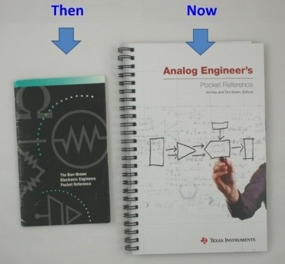
Figure 4: Some things never change
Are there any more things that only an analog engineer would understand? Comment below and let us know if you have any unique experiences in analog.
↧
Modern, sleek and durable touch on metal HMIs
Many industrial and consumer electronic product designers use metal in their designs due to its modern look and durability. However, implementing human machine interfaces (HMIs) on metal surfaces is challenging, as it requires machining and cutting a hole to accommodate a mechanical button. In addition to compromising the aesthetics of the design, mechanical buttons are also prone to failure in moist, dusty or dirty conditions.
Touch through metal allows for sleek touch sensing designs that are waterproof, dustproof, wear-resistant and highly immune to noise. Touch through metal works even when users are wearing gloves and can detect the pressure difference between soft and hard touches, making it a good fit for building security systems, appliances, industrial applications and personal electronics.

Figure 1: Example of dirt and grease proof touch through metal using CapTIvate technology
MSP430™ microcontrollers (MCUs) with CapTIvate™ touch technology bring the flexibility, innovation and reliability characteristic of capacitive touch inputs to applications ranging from appliances to portable electronics. MCUs with CapTIvate technology can implement capacitive touch through metal overlays, allowing highly reliable and sophisticated buttons, sliders and wheels.
In a traditional capacitive touch approach, a touch sensor connected to an MSP430 MCU emits an e-field and detects a change in capacitance when a human finger comes into that e-field. This mechanism works well with plastic, glass and other nonconductive overlay material, but doesn’t work at all with a metal overlay.
MSP430 MCUs with CapTIvate technology use an alternate approach. The stack-up comprises a printed circuit board with traditional capacitive touch sensors and a spacer topped with a grounded metal overlay. This mechanical structure forms a variable capacitor that generates changes in value when a user applies force to the buttons, sliders or wheels. The sensitivity of the integrated CapTIvate peripheral on the MSP430FR2633 family of MCUs allows the detection of a few micron-level deflections of the metal plate.
Because an actuation force is necessary in order to interact with the buttons, metal overlays are waterproof, dirt proof and work even if users are wearing thick gloves. Furthermore, based on the force and amount of deflection, you can implement features incorporating pressure sensing or force on the buttons, sliders and wheels.
The CapTIvate metal touch panel is an add-on board for the CapTIvate development kit. This alternative technology to traditional capacitive touch sensors enables stylish touch module designs using stainless steel, aluminum alloys, brass and bronze. This add-on board features:
- Capacitive touch with metal overlays
- Variable force touch detection
- Multi-key touch
- 7-segment display feedback
- Water, grease and dirt proof
Everything you need for developing your capacitive touch solution, including silicon, software, reference designs, code examples, in-depth documentation, training, and online E2E support, is at your finger-tips at www.ti.com/captivate.
Additional resources:
- Watch this video to learn how capacitive metal touch works
- See a demonstration of the CAPTIVATE-METAL EVM
- Read this application note on touch through metal technology
↧
↧
“Peak current-mode control” in an LLC converter

In 1978, when Cecil Deisch worked on a push-pull converter, he faced a problem of how to balance the flux in the transformer and keep the core from walking away into saturation caused by slightly asymmetrical pulse-width modulation (PWM) waveforms. He came up with a solution of adding an inner-current loop to the voltage loop and let the switch turn off when the switching current reached an adjustable threshold. This is the origin of peak current-mode control.
Since then, peak current-mode control technique is widely employed in PWM converters. Compared to conventional voltage-mode control, peak current-mode control brings many advantages. For example, it changes the system from second order to first order, simplifying compensation design and achieving high loop bandwidth with much better load transient response. Other advantages include inherent input-voltage feed forward with excellent line transient response, inherent cycle-by-cycle current protection, easy and accurate current sharing in high-current multiphase designs.
However, when it comes to inductor-inductor-capacitor (LLC) converters, peak current-mode control becomes infeasible. The reason is obvious: because the resonant current in LLC is sinusoidal, the current is not at its peak when the switch turns off. Turning off the switch at the peak-current instant will cause the duty cycle to be far away from the required 50% for LLC.
Because of this, while peak current-mode control has already been widely used in other topologies, voltage-mode control is still dominant in LLC applications. When power engineers enjoy the high efficiency of LLC, they also experience the poor transient performance caused by conventional voltage-loop control. Because LLC is a high nonlinear system, its characteristics vary with operational conditions. Therefore, it is very difficult to design an optimized compensation, the loop bandwidth is usually limited and the load/line transient response may not be able to meet a strict specification.
Is there any way to employ peak current-mode control in LLC? Let’s take a close look at how peak current-mode control works in PWM converters. In a PWM converter, the switching current is sensed, typically through a current transformer (CT), which is then compared to a threshold to determine the PWM turn-off instant. The CT output is a sawtooth waveform, and the input electric quantity is proportional to the magnitude of this sawtooth wave. This means you are actually controlling the electric quantity going into the power stage. Since the input electric quantity represents the input power, and input power equals output power (assuming 100% efficiency), the peak current mode controls the output power by controlling how much electric quantity goes into the power stage in each switching cycle.
So can you use the same concept in LLC? The answer is yes. One intuitive way is to integrate the input current in each half switching cycle, this can be done by connecting the CT output to a capacitor, where the capacitor voltage represents the integration of the input current. Luckily, there’s already an integration circuit in a LLC circuit. In LLC, when the top switch turns on, the input current charges the resonant capacitor, causing the resonant capacitor voltage to increase. The voltage variation over this half period represents the net input current charged to the resonant capacitor. By controlling the voltage variation on the resonant capacitor, you can control how much input power goes into the resonant tank and thus control the output power.
The UCC256301 adopts this charge-control concept through a novel control scheme called hybrid hysteretic control (HHC), which combines charge control and traditional frequency control – It is charge control with an added frequency compensation ramp, just like conventional peak current-mode control with slope compensation.
Figure 1 shows the details of HHC. There is still a voltage loop; however, instead of setting the switching frequency, its output sets the comparator thresholds VTH and VTL. A capacitor divider (C1 and C2 in Figure 1) senses the resonant capacitor voltage, and an internal current source (ICOMP) charges (when the high-side gate is on) or discharges (when the low-side gate is on) the capacitor divider. Comparing the sensed voltage signal (VCR) with VTH and VTL determines the gate-drive waveform.

Figure 1: HHC in the UCC256301
Figure 2 shows how to generate the gate waveform. When VCR drops below VTL, turn off the low-side gate; after some dead time, turn on the high-side gate. When VCR reaches VTH, turn off the high-side gate; and after dead time, turn on the low-side gate.

Figure 2: Gate waveform in the UCC256301
Just like peak current-mode control in PWM converters, HHC in the UCC256301 offers excellent transient performance by changing the LLC power stage into a single-pole system that simplifies compensation design and achieves higher bandwidth.
Figures 3 and 4 compare the load transient response with HHC and conventional voltage-mode control, respectively. With the same load transient, the voltage deviation is much smaller than conventional voltage-mode control.

Figure 3: Load transient with HHC control

With such superior transient performance, you can reduce the output capacitance while still meeting a given voltage regulation requirement, allowing for a reduced bill of materials count and a smaller solution size.
Additional Resources:
- Watch the video, “Is your LLC resonant controller an underachiever?”
- Read the blog post, “Up your game with LLC resonant controllers.”
- Download the application report, “Improving Transient Response in LLC Converters Using Hybrid Hysteretic Control.”
↧
Industrial radar sensors need 77GHz
Although specialized applications (primarily within the military) have used radar technology for sensing for nearly a century, simplification and size reductions through integration and higher operating frequencies have expanded the use of radar sensing...(read more)![]()
↧
Essential linear charger features
As electronic devices become smarter with more built-in features, they become more attractive but also more power-hungry, making rechargeable batteries an obvious economical choice. Charger requirements have evolved in recent years, with innovative applications, emerging technologies and new battery chemistries. For example, new applications in the wearables space such as smart bank cards, smart clothing and medical patches are driving smaller and cheaper solutions, and smaller and higher-power-density batteries.
Typical questions or concerns from designers include, “How can I maximize battery run time?” “How do I extend my products’ shelf life?” “Is it possible to over discharge the battery?” “What happens if the battery is missing or defective?” “How do I get my product to work with a weak adapter?” and “Can I use the same charger for different designs and different batteries?” In this blog post, I will discuss how different linear charger features can help resolve these issues.
Power path
A power-path function adds one more switch inside the charger, enabling a separate output to power the system and charge the battery. This architecture leads to quite a few other features, but let’s start by looking at Figure 1, which shows a simple linear charger without a power path. The system input and battery terminal connect to the same charger-output node. This non-power-path architecture is popular because of its simplicity and small solution size; examples include the bq24040 and bq25100 battery chargers. Figure 2 shows the bq25100’s evaluation module (EVM).

Figure 1: Simple non-power-path linear charger diagram

Figure 2: bq25100 EVM
This architecture has a few limitations, however. The charger output, battery terminal and system input all connect at the same point. In the case of a deeply discharged or even defective battery, it may not be possible to power up the system even when connecting an external power source. The battery needs to charge to a certain voltage level before the system can power up. Thus, if a product has a deeply discharged battery, the end user may think that the entire system is dead when they plug in the adapter and find nothing happening because the system cannot power up. If the product actually has a defective battery, the system may never power up. For products with removable batteries, it may be possible to remove and replace a defective battery with a different pack. But if the battery is embedded within the equipment, a defective battery will render the entire product useless.
Another issue with this architecture is that the charger only detects the total current going into both the battery and the system. If the system is operating, how can a charger determine if the battery current has reached a termination level?
The solution to all of these concerns is fairly straightforward – you simply add in another switch between the system input and the battery terminal. Figure 3 shows the power-path linear charger architecture. In addition to the Q1 field-effect transistor (FET), which routes current in from the external source, adding one more switch (Q2) decouples the battery from the system when necessary. The system always has the priority of input power, and can turn on instantly when the end user plugs in the adapter. If the adapter has additional power left from supporting the system load, the battery can charge.

Figure 3: Power-path linear charger diagram
This approach also allows the charger to independently monitor the charge current into the battery (as opposed to the total current drawn from the adapter) to allow proper termination and check for any fault conditions.
The bq24072 device family comprises stand-alone power-path linear chargers. The bq25120A is a newer device with more integration. Aside from the power path linear charger, it also integrates a DC-DC buck converter, an LDO, pushbutton controller, and I2C interface for customer programmability.
Ship mode
Ship mode is typically the lowest quiescent current state of a device. Manufacturers enable this state right before a product leaves the factory in order to maximize shelf life, so hopefully the battery is not dead when the end user gets the product. The ship-mode circuit essentially disconnects the battery to prevent battery leakage into the system by turning off Q2 in a power-path charger. When the end user turns the product on for the first time, Q2 turns back on and the battery connects to the system.
Dynamic power-path management (DPPM)
DPPM is another feature on power-path devices. It monitors the input voltage and current of a device, and automatically prioritizes the system when the adapter cannot support the system load. The input source current is shared between the system loading and the battery charging. This feature reduces the charging current if the system load increases. When the system voltage drops to a certain threshold, the battery can stop charging and instead discharge the battery to supplement system current requirements. Implementing this feature prevents the system from crashing.
Input voltage dynamic power management (VIN-DPM)
Another feature usually confused with DPPM is VIN-DPM. The mechanism may sound very similar, but the focus is quite different. Input power sources or adapters have power ratings. There are situations where the input power source does not have enough power to supply what the device demands. Designers are seeing this more commonly now with different USB standards. The device that’s charging may need to work with various (and even unknown) adapter types. If the input source is overloaded and causes the input voltage to fall below the undervoltage lockout (UVLO) threshold, the device will shut down and stop charging. The power-supply load goes away and the adapter recovers. Its voltage goes back up to above UVLO and charging restarts, but the adapter is immediately overloaded again and crashes. This undesirable situation is called “hiccup mode.” See Figure 4.

Figure 4: Hiccup mode
The VIN-DPMfeature resolves this problem because it continuously monitors the input voltage to the charger. If the input voltage falls below a certain threshold, VIN-DPM will regulate the charger to reduce the input current loading and thus prevent the adapter from crashing.
Now you can see that VIN-DPM and DPPM are in fact two very different features. VIN-DPM monitors the adapter’s output (or the charger’s input) and keeps it at a certain level. DPPM monitors the charger output (or the system rail) and maintains it at a minimum predetermined level. These two features can work very well together to allow smooth operation across different operating conditions. Not all chargers have both features. You can implement VIN-DPM on non-power-path chargers as well.
I used the linear charger topology as an example to illustrate some essential features related to power-path functionality, but switching chargers can certainly have this functionality as well. For more information on battery charger selection, see the Battery Charger Solutions page.
Additional resources
- Check out these two other TI E2E™ Community blog posts by my colleague Ming Yu:
↧
Use Ultrasonic sensing for graceful robots
We’re not far from the day when robots perform many of the tasks done by humans today. We already have robotic vacuums cleaning our homes and robotic mowers cutting the grass in our yards. On factory floors, robots are building many of the products...(read more)![]()
↧
↧
FPGA power made simple: design steps
Over the last three installments of this series, I have gone over some basic design considerations for creating a power supply for field-programmable gate arrays (FPGAs). Now that you have determined the power requirements and identified some necessary feature and performance specifications, you are ready to pick parts!
One way to simplify FPGA power if you are a new designer (or strapped for time) is to choose modules as your power supplies. Modules integrate the inductor as well as other passive components to create an easy solution with minimal design. Many of our modules require only three components: the input capacitor, output capacitor and a resistor to set the output voltage. This helps create a small, compact footprint without needing expertise in power-supply layout.
Fewer components not only simplify the solution and reduce the amount of hours needed to design and debug, but also increase reliability. Using a minimal number of components reduces the risk of faulty components or a mistake in the design. TI guarantees many performance parameters in its data sheets, including electromagnetic interference (EMI) performance, thermal performance and efficiency. This means that you can focus less on designing the power and more on adding value to the end product or getting to market quicker.
The disadvantage of a module is that there is less flexibility to optimize the solution through inductor or passive component selection. Modules are typically designed to work with common system architectures, so they are a good option unless you have a particularly stringent performance requirement. Modules can provide good performance and compact solution sizes for most power designs and can be an excellent option, especially for space-constrained, time-constrained or beginner power designers.
Table 1 lists a subset of devices from TI’s power module portfolio that meet the requirements for FPGA rails.

Table 1: Modules recommended for FPGA power
For rails that require large amounts of currents like the core rail, I recommend the LMZ31530/20 or LMZ31710/07/04, which are rated for 30A/20A or 10A/7A/4A, respectively, and meet the 3% tolerance requirement. These devices also have extra features – remote sense to improve load regulation and frequency synchronization, which can help reduce noise and power good for easy sequencing.
For the auxiliary and input/output (I/O), I recommend using TI’s LMZ21700/1 or LMZ20502/1 Nano Modules for the auxiliary rails or general-purpose I/O (GPIO) rails, or the LMZ31704/7/10 if you need higher current. An additional advantage to using Nano Modules is the size advantage. As Table 2 illustrates, Nano Modules in particular provide a very tiny solution size through a small 3mm-by-3mm package and require minimal external components, enabling you to easily save space.

Table 2: Smallest Solutions for Powering I/O & AUX Rails
The transceiver rails are often the most tricky to design for because of the tight noise requirements. Fortunately, all TI modules use shielded inductors and are tested to the Comité International Spécial des Perturbations Radioélectriques (CISPR) 22 Class B standard, which guarantees that the modules meet low-noise requirements. Some TI modules have a frequency synchronization feature to further reduce noise for applications like medical equipment, which is extremely noise-sensitive.
TI provides resources such as reference designs, which provide a ready-made solution that customers can use as a starting point. There is also a tool on WEBENCH® called FPGA Power Architect that can recommend parts and create a full design for you based off of your FPGA and power requirements.
To summarize, when starting a design I recommend starting with these basic steps:
- Use vendor tools to determine your current requirements.
- Check TI reference designs for a ready-made solution.
- Use WEBENCH FPGA Power Architect to create a design.
Following these steps will give you an excellent starting point; you can then continue to optimize the design to meet your exact requirements.
For more information on this topic, check out these resources on FPGA power designs:
- Watch the TI training video, “FPGA Power Made Simple.”
- Browse reference designs featuring Xilinx and Altera FPGAs.
- Read the Power Designer article, “Power Supply Design Considerations for Modern FPGAs.”
↧
“Trust, but verify” SPICE model accuracy, part 5: input offset voltage and open-loop gain
Previous installments of this blog post series discussed the need to verify SPICE model accuracy and how to measure common-mode rejection ratio (CMRR), offset voltage versus common-mode voltage (Vos vs. Vcm), slew rate (SR) and open-loop output impedance (Zo). In part 5, I’ll explain how to verify two of the most impactful specs of precision operational amplifiers (op amps): input offset voltage (Vos) and open-loop gain (Aol).
Input offset voltage
Vos is the difference in voltage between an op amp’s two input pins. Typical offset voltages range from millivolts down to nanovolts, depending on the device. Vos adds in series with any externally applied input voltage (Vin), and therefore can cause errors if Vos is significant compared to Vin. For this reason, op amps with low Vos are highly desirable for precision circuits with small input voltages.
Figure 1 shows the application of a 1mV input voltage to an op amp with Vos equal to 0.1mV. Because Vos is 10% of Vin, the offset voltage contributes a 10% error in the overall circuit output. While this is a fairly extreme example, it shows the impact that Vos can have on op amp designs.

Figure 1: Input offset voltage contribution to DC error
To measure the Vos of an op amp, configure the op amp as a unity gain buffer with its noninverting input connected to mid supply (ground in split-supply circuits). Wire a differential voltage probe between the op amp input pins, and make sure to match the power-supply voltage and common-mode voltage conditions given in the op amp data sheet. Figure 2 shows the recommended test circuit.

Figure 2: Input offset voltage test circuit
Let’s use this circuit to measure the Vos of the OPA189, a new zero-drift, low-noise amplifier from TI. Simply run a DC analysis and observe the voltage at probe Vos, as shown in Figure 3.

Figure 3: OPA189 Vos result
The measured input offset voltage is -400nV, or -0.4µV. This correlates exactly with the spec in the OPA189 data sheet.
Open-loop gain
An op amp’s open-loop gain is arguably its most important parameter, affecting nearly all aspects of linear or small-signal operation including gain bandwidth, stability, settling time and even input offset voltage. For this reason, it’s essential to confirm that your op amp SPICE model matches the behavior given in the device’s data sheet. Figure 4 shows the recommended test circuit.

Figure 4: Open loop gain test circuit
This test circuit is very similar to the one used to measure open-loop output impedance. Inductor L1 creates closed-loop feedback at DC while allowing for open-loop AC analysis, and capacitor C1 shorts the inverting input to signal source Vin at AC in order to receive the appropriate AC stimulus.
As explained by Bruce Trump in his classic blog post, “Offset Voltage and Open-Loop Gain – they’re cousins,” you can think of Aol as an offset voltage that changes with DC output voltage. Therefore, to measure Aol, run an AC transfer function over the desired frequency range and plot the magnitude and phase of Vo/Vos. Make sure to match the specified data sheet conditions for power-supply voltage, input common-mode voltage, load resistance and load capacitance.
Let’s use this method to test the Aol of the OPA189.

Figure 5: OPA189 Aol result
In this case, the op amp’s Aol is modeled very closely to the data sheet spec. The spike in the data sheet’s Aol around 200kHz is caused by the chopping network at the input of the amplifier and is not modeled, although its effect on the nearby magnitude and phase response is.
Thanks for reading this fifth installment of the “Trust, but verify” blog series! In the sixth and final installment, I’ll discuss how to measure op amp voltage and current noise. If you have any questions about simulation verification, log in and leave a comment, or visit the TI E2E™ Community Simulation Models forum.
Additional resources
- Learn more about Vos in Bruce Trump’s “SPICEing Offset Voltage” blog post.
- Watch these TI Precision Labs – Op Amps videos:
- “Vos and Ib.”
- “Bandwidth 1.”
↧
Why a wide VIN DC/DC converter is a good fit for high-cell-count battery-powered drones
More and more drone applications require high-cell-count battery packs to support longer flying distances and flight times. For example, consider a 14-series lithium-ion (Li-ion) battery pack architecture where the working voltage is 50V to 60V. When designing a DC/DC power supply for such a system, one of the challenges is how to select the maximum input voltage rating. Some engineers see an outsized voltage excursion at the node designated VM in Figure 1, but may not be aware of its origin or how to deal with it.

Figure 1: Drone system block diagram
First, let me explain the modes of operation of a motor driver. As shown schematically in Figure 2, the battery stack powers a brushed-DC (BDC) motor, M1, through the forward current path designated as loop 1, and electric power converts to the motor’s rotational kinetic energy during this period. Conversely, when the motor decelerates or changes its direction of rotation, it acts as a generator; the resulting back electromotive force (EMF) returns energy to the input through the driver via current loop 2.
Although this action may seem advantageous in terms of improving overall system efficiency, the regenerative behavior can result in a large reverse current and consequent voltage overshoot at the supply input.

Figure 2: Forward current paths of a BDC motor H-bridge driver
Table 1 outlines typical voltage-rating margins for different motor types. The overshoot voltage range (relative to the nominal battery operating voltage) also depends on the drone’s flight dynamics and control algorithm for the thrust and direction change of each propeller.

Table 1: Motor driver voltage rating requirements
In order to manage this voltage overshoot and ensure that the system runs safely, you can use an electrolytic bulk capacitor for C1 to absorb the energy or, alternatively, add a transient voltage suppressor (TVS) diode to clamp the voltage to a safe range.
Take the Rubycon 2200µF/63V electrolytic capacitor, for example. Its diameter and height are 18mm and 33mm, respectively – quite large to go in a drone implementation where footprint and profile are important constraints. The 1,000-unit price of this capacitor is more than $1.00 from a distributor such as Digi-Key. More important is that this electrolytic capacitor, with its finite rated lifetime, represents an acknowledged limitation in terms of system reliability and robustness. A TVS clamp also creates space, cost and reliability concerns for the whole system.
Another option is to use a DC/DC converter solution with a wide input voltage range and high-line transient immunity to accommodate the full voltage excursion during the motor’s regenerative action.
Selecting a converter with a wide VIN range, such as the LM5161 100V, 1A synchronous buck converter from TI (see Figure 3) enables you to eliminate the bulk energy storage or TVS clamp, saving time, cost and board space. Moreover, the LM5161 converter offers a large degree of flexibility in terms of platform design. Not only does it support a non-isolated output, but the converter can also deliver one or more isolated outputs – using a Fly-Buck™ circuit implementation – if it’s necessary to break a ground loop or decouple different voltage domains in the drone system. If a VCC bias rail between 9V and 13V is available, the LM5161’s input quiescent current reduces to 325µA at a 50V input to uphold battery life during standby operating conditions.

Figure 3: LM5161 step-down converter schematic
Summary
Amid a continual focus on high reliability, small size and low overall bill-of-materials cost, a wide VIN synchronous buck converter dovetails seamlessly into a variety of power-management circuits for drone applications. A proposed DC/DC converter conveniently provides high efficiency performance, topology flexibility and increased circuit robustness during transient voltage events when mechanical energy from the motor cycles back to the input supply.
Additional resources
- Order the evaluation module for the LM5161 100V synchronous buck converter.
- Download the LM5161quickstart calculator.
- Peruse these reference designs for drones:
- Non-Military Drone, Robot or RC 2S1P Battery Management Solution Reference Design.
- Sensorless High-Speed FOC Reference Design for Drone ESC.
- 4.4 V to 30 V, 15 A, High Performance Brushless DC Drone Propeller Controller Reference Design.
- High Density Efficient Solution for Main Aux As Well As Back Up Aux Power in Drones.”
- Review the white paper, “Valuing wide VIN, low EMI synchronous buck circuits for cost-driven, demanding applications.”
↧
SimpleLink™ MCU SDKs: What is an SDK plug-in?
One of the challenges in systems development is expanding beyond the capabilities of your selected microcontroller (MCU). This expansion could include connecting to sensors or actuators to interface with the environment, or connecting to additional controllers or radios for more flexibility or connectivity options.
Developing drivers for these external components to work with your primary MCU can be difficult and time-consuming depending on the architecture, quality of documentation, or availability of code examples. The software framework of your primary MCU also plays a role in the ease of integration of these external components. If primary MCU doesn’t provide clearly defined application programming interfaces (APIs) or if the external component’s drivers do not follow an aligned coding convention, getting the two to communicate effectively can require a number of modifications or writing new code from the ground up. In some cases, it may not even be possible to access the full functionality of the external component.
TI’s SimpleLink™ MCU plug-ins make it easy to extend the functionality of SimpleLink MCUs through common reuse of SimpleLink MCU SDK APIs. Plug-ins are now available for a variety of categories enabling users to add more functionality to their baseline SDK.
- A sensor and actuator plug-in offers intuitive APIs for interfacing with external components such as accelerometers, gyroscopes, temperature sensors and more.
- Connectivity stack plug-ins are available to add new connectivity to a host MCU, including Bluetooth® low energy, Wi-Fi® and more.
- Cloud plug-ins offer easy connections to various IoT Cloud platforms, including Microsoft Azure and Amazon AWS.
Figure 1 is a block diagram of a sensor and actuator plug-in and shows a typical connection with the SimpleLink SDK.

Figure 1: Sensor-to-cloud plug-ins and SimpleLink SDK connections
The plug-ins leverage the well-defined architecture of SimpleLink SDKs, primarily based on TI Driver functional APIs in the SDK and the real-time operating system (RTOS) kernel, for an optimized system-level solution. You won’t waste time trying to modify drivers, identify APIs or create new ones. The software for many external components “plug in” to the SDK seamlessly, leveraging the common APIs and enabling quick setup and communication between the components.
Each plug-in contains all of the necessary components to function fully alongside the SDK. Plug-ins do not install inside of the SDK itself, but rather in a folder next to the SDK. This simplifies the maintenance model and provides an organic experience for updating and switching between plug-in versions. Through the use of highly portable TI driver libraries and standardized Portable Operating System Interface (POSIX) APIs, it is possible for one plug-in to support multiple SDKs. Plug-ins are designed to have a uniform look and feel, as well as a common user experience with all SimpleLink MCUs.
From a hardware perspective, the external components typically available on TI LaunchPad™ development kits or BoosterPack™ modules also connect together seamlessly, as shown in Figure 2.

Figure 2: MSP-EXP432P401R LaunchPad development kit and BOOSTXL-SENSORS BoosterPack module with SimpleLink SDK plug-in support
Each plug-in has been tested and verified against specific versions of the SDK. You can find the compatible versions in the release notes for each plug-in. Complete documentation and SimpleLink Academy online training modules are also available.
SimpleLink SDK plug-ins make it easy to plug in additional system capabilities to enhance and expand your embedded application, freeing you from needless frustration when trying to enable communication between components and enabling you to focus on your application.
Find out more in the SimpleLink SDK plug-ins section of Resource Explorer or on the SimpleLink SDK pages.
↧
↧
ESD fundamentals, part 1: What is ESD protection?
If you’ve seen a lightning bolt or been unpleasantly shocked by a doorknob, you’ve been exposed to the phenomenon known as electrostatic discharge (ESD). ESD is the sudden flow of electricity between two charged objects that come into close proximity. Objects that are in contact sometimes cause a discharge of electricity to go directly from one object to the other. Other times, the voltage potential between the objects can be so great that the dielectric medium (usually air) between them breaks down – contact isn’t even necessary for the electricity to flow (Figure 1).

Figure 1: Electrons transferring between two charged objects result in ESD
These shocks happen all the time, but humans can’t feel most of them because the shock voltage is too low to be noticeable. Most people actually do not start feeling the shock until the discharge exceeds 2,000-3,000V! While ESD in the 1-10kV range is typically harmless to humans, it can cause catastrophic electrical overstress failures for semiconductors and integrated circuits (ICs).
ESD suppressors or diodes placed in parallel between the source of ESD (typically an interface connector to the outside world) and the component (Figure 2) can protect system circuitry from electrical overstress failures.

Figure 2: An ESD strike will damage an IC without ESD protection (left); ESD protection will shunt current to protect the downstream IC (right)
Without ESD protection, all of the current from an ESD strike would flow directly into the system circuitry and destroy components. But if there is an ESD protection diode present, a high-voltage ESD strike will cause the diode to breakdown and provide a low-impedance path to redirect the current to ground, thus protecting the circuitry downstream.
Many circuit components include device-level ESD protection, which has led some to question the need for external ESD protection components. However, device-level ESD protection is nowhere near robust enough to survive ESD strikes discharged onto real-world end equipment. And as chip sets decrease in size due to process innovations, their susceptibility to ESD damages actually increases, making discrete ESD protection a necessity for every circuit designer.
In the next installments of this five-part series, I will go over the different features and requirements for selecting the proper ESD protection diode. In the meantime, get more information on TI’s comprehensive portfolio of protection solutions for ESD and surge events.
Additional Resources:
- Learn more about TI's ESD products here.
↧
Voltage and current sensing in HEV/EV applications
This post was co-authored by Ryan Small.
The rapid increase of semiconductor content in automotive systems has prompted a need to manage key voltages and currents in each subsystem. Supervising supply voltages, load currents or other important system functions can help indicate fault conditions, prevent catastrophic failures and protect end users from potential harm.
Hybrid electric vehicles (HEVs) and electric vehicles (EVs) have some distinct challenges compared to conventional combustion-powered vehicles. HEV and EV vehicles feature numerous systems that require monitoring voltages and currents, including the on-board charger (OBC), battery-management system (BMS), DC/DC converters and inverters. In this post, we’ll discuss the three fundamental circuits for monitoring current and voltage in HEV/EV systems: low-side current sensing with a difference amplifier (DA), in-line isolated current sensing and high-voltage sensing using an attenuating DA.
Figure 1 is a simplified HEV/EV block diagram showing common systems that require voltage and current monitoring.

Figure 1: Typical HEV/EV system
While we won’t cover the operation of the subsystems in this post, designers sometimes use discrete DAs for low-side current sensing (as shown in Figure 2), particularly when the load current is bidirectional or they need a small reference voltage to pedestal the output to a known value greater than the amplifier’s minimum output swing. For the printed circuit board (PCB) layout, you should Kelvin-connect the shunt resistor. It is important to use a device with a common-mode voltage range that includes ground, such as the LM2904-Q1 or TLV313-Q1.

Figure 2: Difference amplifier for low-side current sensing
Equation 1 gives the transfer function for this circuit, assuming R4 = R2 and R3 = R1. The amplifier for this application usually has a common-mode range that includes ground. Depending on the situation, however, the common-mode voltage may not be near ground because it actually depends on the voltage divider created by voltage across the shunt resistor (ILoad*Rsh), Vref and the ratio of R3 to R4. Make sure that the gain (R2/R1) is such that the output-voltage swing does not saturate.

Figure 3 depicts a high-side, in-line isolated current-sensing solution. The AMC1200 is a differential-in, differential-out isolated amplifier. Isolated amplifiers help protect low-voltage circuitry from high common-mode voltages. The DA converts the differential signal to single-ended, which an analog-to-digital converter (ADC) can then digitize.

Figure 3: Difference amplifier used for differential to single-ended conversion, isolated in-line sensing
Equation 2 gives the transfer function for the circuit shown in Figure 3, assuming R4 = R2 and R3 = R1. The gain of the AMC1200 is 8V/V. Vref typically connects to V2/2 to bias the output to mid supply to support bidirectional current. A rail-to-rail input/output (RRIO) amplifier such as the TLV313-Q1 is a good fit for this application.

Figures 4 and 5 depict an attenuating DA and the corresponding TINA-TI™ simulation. In this circuit, the DA resistors divide the input voltage (±100V) down. Since the input voltage is bipolar, a reference voltage set to mid supply biases the output. When selecting the amplifier, be sure to comply with the device’s input common-mode and output-voltage swing specifications. This example utilizes the OPA314-Q1 because of its wide common-mode range.

Figure 4: Attenuating difference amplifier

Figure 5: TINA-TI software simulation of attenuating difference amplifier
Equation 3 gives the transfer function for the circuit shown in Figure 4, assuming R4 = R2 and R3 = R1. Notice that the gain is less than unity.

In this blog post, I presented three common circuits that appear in automotive subsystems such as the OBC, BMS, DC/DC converters and inverters. Additionally, I highlighted that HEV/EV applications use voltage and current sensing to monitor critical system functions, helping to maximize vehicle lifetimes. To learn more about the key operational amplifier specifications mentioned in this blog (for example, common-mode voltage) check out TI Precision Labs.
Additional resources
- For additional information on PCB layout, read these blog posts:
- “The basics: How to layout a PCB for an op amp.”
- “How to layout a PCB for an instrumentation amplifier.”
- Watch the video, “TI Precision Labs – Op Amps: Input and Output Limitations.”
- Find common analog design formulas in the “Analog Engineer’s Pocket Reference.”
↧
How to use load switches and eFuses in your set-top box design
Sitting in front of a TV is easy. Changing the channel is easy. Recording four shows at once while watching one show on your TV and streaming another show to your tablet is excessive – but also easy! It’s all thanks to the power of set-top boxes (STBs), such as the one shown in Figure 1.

Figure 1: A typical STB
STBs take in a cable/satellite signal; translate that signal into video; and then transmit that video to a TV, hard drive or wireless device. Designing these systems can be complicated but designing the power distribution can be easy, especially when you use load switches and eFuses.
Why bother turning different loads on and off?
STB designers usually follow standby power requirements so they can improve the system’s power efficiency. These requirements limit the amount of power that the STB can draw when it is inactive, so different subsystems need to be off in order to draw a minimal amount of power. Some regions even have specific power requirements, such as such as Energy Star. Figure 2 shows the common STB subsystems that can be controlled to improve standby power.

Figure 2: Load switch and eFuse applications in STBs
Now let’s take a look at some of the subsystems you can switch on and off.
- Front end/tuner. This subsystem takes the input signal (cable or satellite) and converts the signal into video. One tuner is responsible for a single video output, so if an STB can record five shows at once, that means that there are five different tuners dedicated to recording. Likewise, there is a tuner for the output video port and for connecting additional devices through Wi-Fi®. Switching the tuners off when they are not being used can reduce shutdown power.
- Hard drive. A hard drive that is not recording a show or playing a previously recorded show does not need to be active. This is also the case when the STB is just outputting the cable signal.
- Wi-Fi. Wi-Fi connects additional devices to the STB such as tablets or computers, or connects smaller STBs within the same household.
Load switches can control power to each of these subsystems, and both the TPS22918 and TPS22975 can be used depending on the current load. Both are plastic devices that come with an adjustable output rise time suitable for different capacitive loads. The TPS22918 can support loads up to 2A and the TPS22975 can support loads up to 6A.
What about using switches for additional features?
Aside from power savings, several other features require a switch:
- Power sequencing.The system on chip (SoC) or microcontroller that controls the STB has a specific power-on sequence for its different voltage rails. For optimal performance, devices like the TPS22918 or TPS22975 can turn on each of the rails in order.
- Input protection.Voltage and current transients can occur when the 12V adapter is plugged into the STB. Placing the TPS2595 eFuse at the STB input can protect the rest of the system from hot-plug events.
- SD card. If an STB uses an SD card, the option exists to power it with 3.3V or 1.8V. Using the TPS22910A and TPS22912C load switches enables you to choose the appropriate rail.
- HDMI. The HDMI port is powered with 5V when in use, and the current needs to be limited for user protection. The TPS22945 load switch has a low current limit of 100mA.
All of these applications are modeled in the block diagram in Figure 3.

Figure 3: Recommended load switches and eFuses in STBs
Where can you get started?
The Power Switching Reference Design for Set Top Box shows all of the different load switches and eFuses used for each subsystem. With the added DC/DCs, the design helps create a complete solution for STB power delivery.

Figure 4: Power Switching Reference Design for Set Top Box
With the trend in STB moving to smaller form factors, it’s easy to see why designers are looking for more integration in their systems. So keep your STB power design small and easy, and use load switches and eFuses to accomplish your varying power switching needs!
Additional resources
- Only have a few minutes? Watch some videos:
- “Load Switches vs. Discrete MOSFETs” (2:35).
- “Load Switches vs. Discrete MOSFETs – Problems with a discrete solution and how a load switch can fix them” (3:22).
- Learn more about load switches by downloading these application notes:
- “Load Switches: What Are They, Why Do You Need Them and How Do You Choose the Right One?”
- “Integrated Load Switches versus Discrete MOSFETs.”
- Check out the following load switch blog post for more information:
↧