Quantcast
Channel: TI E2E support forums
Viewing all 4543 articles
Browse latest View live

Pit ninjas, robots, mentors and teamwork: Journey to robotics competition teaches value of STEM education

$
0
0

(Please visit the site to view this video)

Members of the robotics team at Conrad High School Juan Salagado is the pit ninja. He taught himself to code and became so fascinated by it that he helps other teams during competitions. Javi Calderon, a member of the National Honor Society, is the 3-D printing expert and manages data analysis. He and his friends compete to see who can earn the highest grade-point average. Annette Morales, a go-getter and Student Council president, is known for her drive and organization skills.

All are members of the robotics team at Conrad High School in the Dallas Independent School District. With help from mentors, including several from our company, the team has grown into a powerhouse that this year placed seventh in its division in the FIRST® Robotics Competition (FRC) World Championships in Houston.

“A robot is made up of gears, circuits and sensors that all have to function together seamlessly for the robot to work,” said Bart Basile, an engineer at our company and a mentor for the team. “Our team operates the same way, with all of the members bringing their unique skills together to compete in robotics events.”

Until recent years, Juan, Javi, Annette and other members of the Conrad team could only dream of going to a world robotics competition. In the early days, the team had few tools or mentors and built its robots in the back of a classroom. Many have backgrounds where going to college isn’t an option.

But with TI’s help, things changed. Doors opened. The team now has a well-equipped shop and competes at the international level. The students from Dallas – many of whom now have college plans – have become a team to watch.

Learning new things every day

Members of the robotics team at Conrad High School The team’s journey to the world championships started Jan. 6. That Saturday morning, thousands of students and mentors gathered in locations around the world for the announcement they’d been waiting months to hear. The Conrad team, along with hundreds of other area high school students, met at our company’s headquarters in Dallas to watch the kickoff. As soon as this year’s challenge was announced, the team set off to start building, spending the rest of their Saturday in the school’s shop.

Over the next few months, they met every day after school to design, program, code and build the robot. The students, teachers and mentors spent many long evenings and hundreds of hours together, determined to make this year their best yet.

“Working with the robotics team keeps me busy,” Javi said. “My parents used to think it was weird that I wanted to stay after school. But I get to learn new things almost every day. That’s why I love it.”

Growing up together

Team members got their first chance to compete in March, during a FIRST® Championship regional event in Irving, Texas. They came in third out of 60 teams.

The team members then traveled with their teachers and mentors to Denver for another regional tournament. They won a coveted blue banner for being part of a winning alliance. 

Members of the robotics team at Conrad High School

“It was so exciting,” Joel Lopez, one of the Conrad team members, said. “We blew through the competition and made it to finals. We had a really tough alliance, and we won first place. We got our first blue banner. It was an amazing, emotional feeling for everybody.”

Finally, in April, it was time for the FIRST Championship in Houston. Team members competed against more than 400 teams from around the world. They ranked No. 7 in their division, and were invited by the No. 2 seeded team, former world champions, to join its alliance.

“We felt like it was a breakout year,” said Steven Smith, an engineer at our company and a mentor for the team. “Even though we didn’t place as high in the final tournament as in previous years, we felt a buzz from the robotics community. It was exciting. Teams from around the nation – some of the best teams in the world – were coming up to us and saying that they liked our robot or commenting on things we did well. Our kids took a lot of pride in that.”

Engineering their future

Members of the robotics team at Conrad High School With six seniors, two juniors, eight sophomores and nine freshmen, it would be hard to showcase everyone’s talent, but Bart and Steven –  along with several other mentors – work hard to make sure everyone has a role.

“Each person on the team contributed to what was our strongest year yet,” Steven said. “There is a team behind every student. It’s not one single accomplishment or person. It’s a combined effort that really made this team stand out.” 

Mentors are critical to the team’s success.

“As mentors, we were able to help them get a workshop space at the school, and it really grew from there,” Bart said. “Now they have a dedicated room with computers, a full machine shop, 3-D printers, and piles of spare parts and material. They can really let their imaginations run when they want to build something.”

“The time and dedication that Bart and Steven put into the team is amazing,” Joel said. “There was even a time that Steven stayed at the school all night, working into the morning, even though he had a flight to China the next day for work. Having mentors from TI helps make us a really successful team.”

For Bart, one of the most rewarding reasons to be a mentor is watching students develop into individual roles and build camaraderie. 

“I started out showing them what to do,” he said. “But now we’ve put together a sustainable program with students teaching students. As a mentor, I’m more hands-off now and trust the students to take the lead and educate their peers. Now we have students choosing to go to school at Conrad because of the robotics programs. They come in and know what they want to work on.”

Our company has about 75 active mentors and volunteers worldwide working with high school robotics programs in our communities, but there is a growing need for more as their popularity increases.

“We’re always looking for more mentors and volunteers,” Bart said. “The FIRST motto is, ‘It’s way more than building robots,’ and it really is so much more. You get to see these kids challenge themselves and realize everything they can accomplish together.”

For many of the students, being part of the team is an opportunity to experience what it means to have a career in engineering. FIRST® is designed to inspire young people’s interest and participation in science and technology and to motivate them to pursue education and careers in STEM fields. It’s become a global movement, engaging millions of students, teachers and mentors, and giving them hands-on robotics experiences.

More than building robots

Conrad High School Learning extends far beyond technical skills. Students are responsible for writing and submitting entries to competitions, presenting to judges, and budgeting for projects and expenses.

“People think of math and science when it comes to robotics, but communications plays a big part,” Joel said. “When you’re talking to people at competitions all the time, it takes the shyness out of you and you learn communication skills. But we’re also writing essays and resumes for competitions, and that can help you get into college.”

They are also building relationships and learning how to work as a team.

And college is on the horizon for some. Joel is going to the University of Texas at Dallas to study manufacturing engineering. Juan plans to attend a local community college as he plans for the future. Annette and Javi are going to Texas A&M University. Javi plans to study veterinary science and wants to apply robotics to the field.

“We see a lot of these kids come from under-served families and communities,” Bart said. “Robotics motivates them to understand that they can go to college. But they also come out with a set of skills they can do something with. In their communities, they may not have access to an engineering role model. We can help provide that. As long as they came out learning something valuable to them, it’s worth it.” 

Learn more about FIRST Robotics and TI’s commitment to robotics programs.


New WEBENCH® Power Designer is now even easier to use

$
0
0

TI is committed to continually improving the online design experience. On July 5, we will introduce our new fully redesigned HTML5 application for WEBENCH® Power Designer. In this post, I will walk you through the new enhancements, designed to help you make power design decisions faster and easier.

The input form

The first thing you’ll notice is our new re-designed input form displayed in Figure 1 below. You can use this form to quickly look up a TI device that you may have in mind or start your search using basic inputs. The advanced settings are now organized to guide you toward designs meeting any criteria, and the optimization knob is now a Design Consideration toggle

.

Figure 1: Re-designed input form

Select a design screen

The first step in the power design process is to select your design. WEBENCH Power Designer previously calculated operating values and generated a thumbnail of what the schematic may look like. New optimized algorithms now enable you to generate full power designs. Our large selection of filters lets you narrow down which design would best fit your needs. For users who are used to the original flash version, there’s still a table view option. However, a new card view, pictured below in Figure 2, is the default view in the selection step.

This card view has additional features that enable you to:

  • View and download actual design schematics, bill of materials and operating charts.
  • Click to compare multiple designs side by side.
  • Link directly to more information and make a purchase.
  • When logged in, the ability to share designs and print a WEBENCH PDF design report.

Figure 2: Select screen card view

The compare designs feature

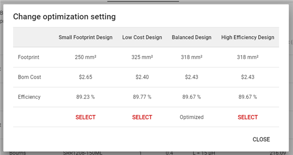
Figure 2 above shows the new selection screen with check boxes on each design to compare designs. This new feature generates a table, displayed in Figure 3, with additional information such as integrated circuit (IC) parameters and IC features which enables a side-by-side comparison of multiple designs.

Figure 3: Select screen compare popup

New layout

The customize, simulate and export design steps from our former version of WEBENCH Power Designer have been split from a single screen into three new screens, with logical steps to guide you through the power design flow.

Figure 4 below is a screen shot of the new Customize screen.  You will notice that you can view your design upfront, customize parameters to the left, and see the effects of your customizations in operating and performance below.  You will also see in Figure 5 that we have removed the optimization knob. The removal of the optimization knob simplifies the process by calculating the design values upfront for comparison purposes so that you can make the best decision to meet your optimization needs.

Figure 4: Customize screen


Figure 5: Optimize your design

Once you are done customizing, you can verify your design by running an electrical simulation in the next screen.  Finally, you can move on to the export screen which displays an overview of your final design with clear buttons to prompt you to export to your most used CAD tools, print a design PDF report, or circle back to TI.com for more information such as downloading a datasheet, going to the TI Store, or exploring the product folder.

Mark your calendars for our July 5 launch date and subscribe to TI’s Power House blog community for further content on how to best navigate our new interface.


Thread vs. Zigbee – What’s the difference?

$
0
0

Standards like Wi-Fi and Bluetooth low energy have become synonymous with the rise of “smart” devices in our homes that are controlled by digital assistants (such as the Amazon Echo).  These standards are popular and well known to consumers. However, as the number of connected devices in our homes, buildings and cities grows, other lesser-known standards, like Thread and Zigbee, are becoming more relevant.  The growing number of these technologies has brought the challenges of significant design complexity, including selecting which wireless protocol to use. The choice of which wireless technology to use for a deployment ultimately depends on several factors:

  • Whether the device is battery-powered.
  • Its form factor.
  • The type of application it will support (streaming a high frequency of messages or infrequently sending and receiving commands).
  • Integration with existing ecosystems.

Today, many communication technologies enabling device-to-device, device-to-cloud and device-to-mobile communication are at the heart of home and building automation, including Wi-Fi®, Bluetooth® low energy, Sub-1 GHz, Thread and Zigbee®. However, for this blog post, I’ll focus on some of the key advantages and differences of Zigbee and Thread.

What are Thread and Zigbee?

Thread and Zigbee are low-power, wireless mesh standards that target embedded home and building automation applications. Both protocols leverage the Institute of Electrical and Electronic Engineers (IEEE) 802.15.4 standard, which specifies the lower layers of the Thread and Zigbee protocols (the physical layer [PHY] and media access control [MAC] layers).

Since the upper-level layers are implemented in software rather than hardware (shown in Figure 1), Thread and Zigbee can be deployed as different software variants on top of common hardware, like the SimpleLink™ multi-standard CC2652R wireless microcontroller (MCU).

Figure 1: Zigbee and Thread protocol layering.

Both Thread and Zigbee are driven by industry-level alliances that push the protocol development forward and certify products out in the market.

Thread vs. Zigbee

One of the key differences between Thread and Zigbee is that Thread leverages Internet Protocol version 6 (IPv6), which enables a natural connection between Thread networks and existing IPv6-based networks like Wi-Fi. Zigbee, however, was built from the ground up, and each node in the network gets a 16-bit address that must be translated into IP using an application layer gateway.

Another key difference between the two standards is that Thread does not define specific application layers, while Zigbee defines all layers in the OSI model. This makes Thread a more flexible choice in terms of application layer selection. On the other hand, since Zigbee specifies application layer, a greater interoperability on application layer is guaranteed.

There are also some differences in authentication process between the two protocols. Thread authentication and commissioning is smartphone-based, while with Zigbee, authentication is centralized through a trust center with proximity-based commissioning.

The last key difference between the two protocols is longevity. Thread was first released in 2015, but Zigbee has been around since 2005. Today, Zigbee has much greater market penetration and a larger industry forum. Thread is still relatively new and still in the “adoption” phase. Details of the differences between Zigbee and Thread are highlighted in Figure 2.

Figure 2: Zigbee and Thread comparison

The good news is that with TI’s SimpleLink MCU platform, you don’t have to choose between Thread and Zigbee when deciding on hardware. The SimpleLink multi-standard CC2652R wireless MCU supports both standards, and with the SimpleLink CC26X2 software development kit (SDK), application code is portable between the two standards.

Be sure to read the white paper, “Thread and Zigbee for home and building automation,” for a deeper dive into the advantages and differences of these two standards.

How to modify a step-down converter to the inverting buck-boost topology

$
0
0

 When looking for a DC/DC converter to create a negative voltage, in many cases you will use a step-down converter in the inverting buck-boost topology. While dedicated inverter devices such as the very-low-noise TPS63710 are easier to design with and generally a better solution, there are numerous reasons to use a step-down converter as an inverting buck-boost converter instead. First, there are relatively few dedicated voltage inverter devices in the market, compared to the ubiquitous step-down converter. You may not find a specific feature or characteristic which is required in your application. In other cases, it greatly simplifies the procurement effort to use another instance of an existing step-down converter for another socket in the design through utilizing it in the inverting buck-boost topology. Since there are generally very few inverting buck-boost circuits available for lab testing, you will need to modify the readily-available step-down converter EVM into the inverting buck-boost topology to measure the circuit for your design. This blog walks you through the steps required to take the standard TPS82130 evaluation module (EVM), which is configured as a step-down converter, and create an inverting power supply based on  3- to 11.5-VIN, –5-VOUT, 1.5-A Inverting Power Module reference design.

Using a step-down converter as an inverting buck-boost converter is a valid application use case, supported by numerous reference designs and applications notes. The TPS82130 step-down power module is used as the example, because of its high integration level and simple design. It also contains two inverting buck-boost reference designs, TIDA-01457 and TIDA-01405, with full test data and documentation. Please see the reference design guide section 2.3 for a detailed technical discussion of using step-down converters as inverting buck-boost converters.

To begin, Figure 1 shows the standard EVM as it would be connected as a step-down converter.

Figure 1: TPS82130EVM-720 connected as a step-down converter

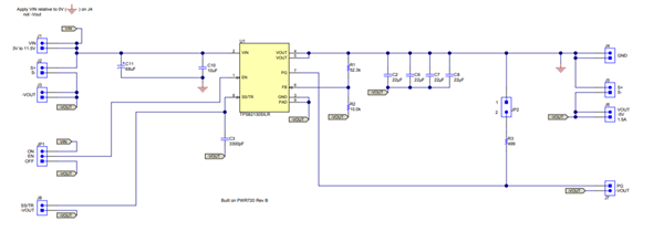
To achieve the TIDA-01457 design, its inverting schematic in Figure 3 is compared to the normal step-down EVM’s schematic in Figure 2. 

Figure 2: Step-down converter (TPS82130EVM-720) schematic

Figure 3: Inverting buck-boost (TIDA-01457) schematic

To achieve the inverting function, the output terminals are swapped such that VOUT (J4) becomes GND and the GND terminal (J6) becomes –VOUT. Everything that was GND is now labeled –VOUT. In addition, the input voltage is applied from VIN to VOUT, which is now GND.

Further comparing the two schematics, we find the remaining changes required to transform the EVM into the inverting circuit. Note that the reference designators are identical between the designs, except for the input capacitors C1 and C4 whose connections need to change from what the existing printed circuit board (PCB) provides.

Here are the required changes, which are shown in the following images:

  • Remove C1 and C4, but save them to re-install later
  • Install a 22-µF ceramic output capacitor at C6, C7, and C8
  • Change the value of R1 and R2 to set the appropriate output voltage
  • Install the input capacitors, C10 and C11, which were saved from earlier

First, the input capacitors are removed, the additional output capacitors installed, and the two feedback (FB) resistors changed.  Figure 4 shows the resulting EVM:

Figure 4: TPS82130EVM-720 partially modified to an inverting circuit

Next, the input capacitors, C10 and C11, are installed. There are no pads at the correct electrical locations on the existing EVM, so the existing pads for the VIN connection are used and a wire is added to complete the connection to GND, which is VOUT on the PCB. Figure 5 shows the result, which has completed all modifications and is now an inverting buck-boost power supply.

Figure 5: TPS82130EVM-720 completely modified to an inverting circuit

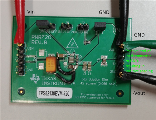
Figure 6 shows this same EVM wired in the correct way and ready to be powered on. Note that the positive terminal of the load connects to GND (J4) and the negative terminal to GND (J6). This presents the load with a positive voltage, instead of a negative one.

Figure 6: TIDA-01457 connected as an inverting buck-boost converter

These same steps and procedures are applicable to most step-down converter EVMs and allow you to quickly evaluate them as inverting buck-boost converters, without having to make a PCB of your own.

Additional Resources

Browse TI’s inverting charge pump solutions

Browse TI’s inverting buck-boost solutions


Predicting motor failures with vibration analysis, Part 2

$
0
0

Motors and pumps are key infrastructure components in both factories and buildings and must be maintained in proper working condition in order to perform their tasks. These tasks may range from moving objects on an automation line to transporting cooling fluids/air for heating, ventilation and air-conditioning (HVAC) systems.

At any time, a drop in performance may result in costly maintenance or downtime for your production capability. To maintain satisfactory performance, it is vital to monitor these machines for indicators of potential failures, some of which may not be observed by human senses but by low-power and smart sensor solutions deployed as part of a production infrastructure.

Vibration analysis for motors

Humans can listen for the condition of a moving element when the system is close to a breakdown. However, the same element may not produce an audible noise, or perhaps the noise is not easily detectable because of the environment it’s in, like a noisy factory floor or motor housing. The Figure below shows the construction of a motor bearing.

Figure 1: Internal view of a motor bearing

The mechanical construction of a motor bearing comprises:

  • The inner race – the inner surface of the moving element, which is typically mounted on the shaft.
  • The outer race – the outer surface of the moving element; this is a static component.
  • The cage – holds the ball bearings in place.
  • Rolling element “balls” – the moving elements between the inner and outer races.

The elements of a motor outside of its housing may consist of a shaft, gears and/or mounting posts.

The onset of a fault will result in small mechanical deformities. When the moving elements of a motor make contact with these deformities, as a result of repeated and consistent impact between two surfaces, the faults manifest themselves as shock pulses.

Fortunately, each of these shock pulses has a relation to the rotational speed of the motor, expressed using rotations per minute (RPM). This means that any onset of a mechanical fault can be expressed as an equation. For example, the ball bearings moving over a fault on the inner race produces a defect frequency called the ball pass frequency of inner race (BPFI), which is different from the defect frequency generated when the ball bearings move over a fault on the outer race, which is called the ball pass frequency of outer race (BPFO).

You can calculate BPFI and BFPO using Equations 1 and 2, respectively:

BPFI = (NB× S) × (1 + (BD x cos θ) ÷ PD) ÷ 2                               (1)

BPFO = (NB× S) × (1 - (BD x cos θ) ÷ PD) ÷ 2                              (2)

Where NB is the number of balls, S is the revolutions per second (RPM ÷ 60), BD is the ball diameter, PD is the pitch diameter and θ is the contact angle of the ball to the race.

The parameters provided by NTN Bearing Corporation for deep groove ball bearings with the bearing number 16001, result in a BPFI of 4.93 and a BPFO of 3.07 for the S value. Thus, for a 3,600 RPM motor or S = 60Hz, the BPFI is 295.8Hz and the BPFO is 184.2Hz.

Knowing these frequency values is great, but how do you detect a potential motor failure? The answer lies in the shock pulse itself. Using a multiaxis microelectromechanical (MEMS) accelerometer, you can detect shock pulses, translate the vibration into an electrical signal and then intelligently process the signal.

The Reference Design for Wireless Condition Monitor for Motors and Pumps Using Multi-Axis Vibration is an example of such a vibration sensor (see Figure 2). It uses an analog three-axis accelerometer that is measured by the precision analog-to-digital converter (ADC) of the SimpleLink™ MSP432P4 host microcontroller (MCU). The sensor node processes the measured data by generating a fast Fourier transform (FFT) of it.

Figure 2: Wireless condition monitor reference design block diagram

An analysis of the resulting frequency domain data, which can detect these frequency values, can be transmitted wirelessly via Bluetooth® low energy to a gateway, smartphone or tablet. On-site operators can use the data from the sensor directly for diagnostics and troubleshooting. In the cloud, you can store the data and perform further analysis based on previously captured historical data. Depending on the system requirement, additional wireless protocols like Zigbee, 6LoWPAN and wireless mesh are also possible for transmitting the data.

Similarly, every component of the motor assembly produces a different defect frequency or pattern. Being able to nonintrusively monitor a motor and know what frequencies relative to the RPM of the motor to look for enables operators to detect failures proactively.

Conclusion

The ability to isolate and identify frequency patterns for motors and pumps in automated environments ranging from factories to homes helps provide early indication of failure for motors and pumps, resulting in cost and time savings for operators and users. With intelligence and wireless connectivity at the edge node and learning algorithms on the cloud, it’s possible to integrate an automation infrastructure in an ever-increasingly connected world.

Additional resources

  • To get up to speed on the integrated precision ADC of the MSP432P4 host MCU, see these application reports and blog posts:
  • To help you develop wireless connectivity solutions and understand predictive maintenance download the following resources
  • To help you develop wireless connectivity solutions for the MSP432P4 host MCU, see the examples in:

10 lessons learned from 50-plus biometric wearable product development cycles

$
0
0

This is the second in a three-part series on optical heart rate sensors for biometric wearables. The first installment focused on how these sensor systems work and what you can measure with them.

You’re sitting in a planning meeting. The team has just come up with some pretty amazing ideas for the new wearable device with an optical heart rate sensor that you’re adding to your product line. They all turn to you: Who should we partner with for the sensor system? Suddenly you realize that you’re not entirely sure where to begin.

At Valencell, we’ve heard this before — many times, having been involved in more than 50 biometric wearable projects. Valencell uses the AFE4410 in its next-generation Benchmark sensor system and our technology is integrated into more than 20 different biometric wearable devices on the market today. We’ve made some mistakes, learned a lot from those experiences and had some successes along the way. Here are the top 10 lessons we’ve learned throughout the process that you should consider when selecting a biometric sensor system for your next wearable.

1. Get proof that it works before you get started. This might seem pretty obvious, but anyone who has brought a biometric wearable to market will tell you the hardest part of the product development cycle is getting the biometric sensor system to work well enough to meet your requirements. Your starting point should be a working reference design, similar to the one in Figure 1. And don’t just test it on the bench. Put it on at least 20 people and see if it works in your intended use case, compared to a legitimate benchmark device. Another option is to test other companies’ products in the market that are using a particular vendor’s technology. Are their customers pleased with the performance? How does it perform in your tests?

Figure 1: Test a working reference design for biometric wearables

2. Work with a technology provider that knows your market and can support your requirements. Applications for biometric wearables are broad. Make sure your technology provider has the capabilities and experience to deliver on the device you want to build. The right form factor, the right metrics, the right levels of accuracy and the right user experience all play huge roles in a product’s success.

3. Work with a technology provider that has expertise in biometric wearables and optomechanics. Hardware components and optomechanical design are critical factors in accurate biometric wearables. The provider you select should have extensive hardware and optomechanical expertise, and should be experts in evaluating the performance of analog front ends (AFEs) for signal processing, like the TI AFE4410. They should understand how light couples to and from the body to optimize the signals indicating blood flow and minimize environmental noise. A strong team will be sure that the right wavelengths are being used for the chosen device body location and form factor.

4. Advanced signal-extraction methodologies are critically important. Because of the complexities in individual bodies, it’s critical for all technology developers to have a keen understanding of signal extraction algorithms, particularly something called active signal characterization (shown in Figure 2), which identifies and characterizes both motion and environmental noise that can corrupt signals. Isolating these factors, and others, enables the biometric sensor system to report accurate data.

Figure 2: Signal processing involving active signal characterization is critical

5. Advanced biometric measurements are required. Basic heart rate measurement is quickly becoming a minimum requirement for wearables. More advanced metrics will define the future, so take a serious look at what metrics you can get from the system. Does it support continuous heart rate or just take spot measurements periodically? Can it deliver more advanced metrics like beat-to-beat (RR) interval (heart rate variability [HRV]), breathing rate or blood pressure? And, perhaps more importantly, can the vendor prove to you that they can deliver those metrics? Actions speak louder than words.

6. Work with a technology provider who can test your product appropriately. When you partner with vendors for core components of your product, it’s important to know not only how they test their own work, but also how they test their product within your device. If they offer prototype testing services, you’re heading in the right direction. But be sure to ask if they can test your intended use cases, shown in Figure 3. How and where do they conduct that testing? How many people do they test in each round of prototyping?

Figure 3:  Ensure you test the device extensively on the intended use case.

7. Look for proven experience in getting biometric wearables to market. It’s critical to understand what other products on the market are using the tech you’re looking at including in your product. Analyzing consumer reviews of those devices can give you critical insight into how that component will work in your device. How accurate are those products? Are the product reviews positive — at least as they pertain to the heart rate monitoring and biometrics component?

8. Choose a team with multi-disciplinary expertise. You should get an understanding of the skills and expertise of the vendor’s team. Do they specialize in hardware? Optics? Firmware? Algorithms? What are their core competencies?

9. Manufacturing partner experience is highly valuable. Building a biometric wearable is a substantially different project than a typical wearable product, primarily because of the optomechanics involved. Even if you’ve designed and built activity tracking wearables before, don’t underestimate the complexity of adding optical biometrics. You should choose a contract manufacturer that has experience building biometric wearables at scale. They will have faced and solved many unforeseen challenges that other manufacturers have not.

10. Evaluate the intellectual property (IP) landscape. Despite being a relatively new space, there is an extensive patent landscape in biometric wearables and high-profile companies are litigating in this space. The IP landscape for biometric wearables includes areas such as optomechanical designs, data processing, data assessments and visualization of wearable data. Figure 4 highlights the recent trends in wearables patents granted. 

Figure 4:  Wearables patents granted and submitted (photo courtesy of ipwatchdog.com)

I hope this helps you select the right biometric sensor system. The next installment in this series will cover different devices and biometric sensor system use cases.

Additional resources

Qualification on a Noisy Input Signal

$
0
0
In my last post , I talked about how to interpret a CW/CCW pulse train output (PTO) for motor control on C2000™ Piccolo™ F28004x devices. In this post, I will discuss a situation in which you must deal with noisy signal interference on an...(read more)

From internship to mentorship, Moe Garcia builds close-as-family talent pipeline from University of Puerto Rico at Mayagüez

$
0
0

Moe Garcia

Surrounded by swaying palm trees, steps from white sand beaches and in proximity to his family and friends who still live on the island, the work that brings Moe Garcia to the University of Puerto Rico at Mayagüez (UPRM) several times a year might seem like an idyllic assignment. But it's the chance to give back to his school and our company that has driven him to stick with it for eight years.

"It's very fulfilling to help out students at the university,” said Moe, a systems and applications manager. “They’re highly valued by our company, so it’s important for us to give them a closer look at industry work experience.”

Moe has a passionate commitment to the 20-year partnership between UPRM and our company. As campus manager since 2010, He brings our engineers to the campus for talks, arranges scholarships, and coordinates our participation in an "Industrial Affiliates Program" that provides mentorship and funding for student projects and helps to get needed equipment, parts, and tools for UPRM's engineering labs. His strong relationships with faculty have paid off for TI as well as for the students.

"Moe’s efforts have brought talented engineers to our staff who help make our company a more culturally diverse place to work,” said Carrie Hunter, a recruiting manager at our company. “He has such an influence and a strong trust with the professors. Their students are excited to work on the cool, innovative projects that we offer through our summer internships and rotation programs. It's a win-win."

An ever-expanding family

Born and raised in Puerto Rico, Moe earned his electrical engineering degree from UPRM in 2000. As a student there, he worked on TI projects with Professor Rogelio Palomera before securing a seven-month internship at our Dallas headquarters, followed by a full-time job as a test engineer. Now, he’s helping students follow in his footsteps, and growing a pipeline of diverse talent at our company.

"Since UPRM's bachelor of engineering degree is a distinguished five-year program, we're essentially getting master's level students from a bachelor's degree program, and the Mayagüez campus is known for STEM,” Carrie said. “These students have dozens of companies recruiting them."

Under Moe's management, the TI-UPRM family has continued to expand. In 2000, he was our company's third hire from the school. Today, at least 60 UPRM graduates work here. In 2017 alone, 17 students from the campus accepted offers to join us. Counting those who've done internships and moved on since hiring, Moe estimates 100 UPRM engineers have joined us over the course of our partnership.

“The students have questions and are nervous about the interview process,” Moe said. “Some students who I guided through the process now work at TI, are married with children and set up meetings with me to get mentoring on their next career move. It's a family-type relationship with some history behind it that I feel proud of."

Lyanne Magriz Cortes, a physical verification engineer, attests to the close-as-family relationship. She was doing undergraduate research for the SPICE modeling lab in Mayagüez when she met Moe.

"I was majoring in electronics and semiconductors and TI was top in the world,” she said. “There was no doubt I wanted to work here. Since I've joined TI, Moe has been very influential. He's a mentor and a very resourceful person.”

Moe has been known to help UPRM interns with travel arrangements and even helped an intern in a medical emergency to fly home. On the UPRM campus, things are even more familial. Other early hires from the university often join Moe’s missions to the campus for support and to give technical seminars, including Charles Parkhurst, a senior analog design engineer and the very first intern our company hired from UPRM . "They're like the right-hand men," Moe said. During their visits to Mayagüez, Professor Palomera treats them like his own grandchildren and his wife makes dinner reservations and plans the menu.

“Those dinners are more like family meals than professional meetings,” Moe said. "We include spouses, and on one trip I took my daughter and Charles took his son," he says.

A new lab on campus

Coinciding with the 20-year anniversary of the TI-UPRM relationship, our company sponsored a total renovation of UPRM's integrated circuit design laboratory. The newly-reconstructed lab was set to open last fall when Hurricane Maria struck. With minor damages repaired, the formal ribbon cutting and celebration took place this May.

Charles also attended the 20th anniversary celebration in Mayagüez. He says Moe, with whom he shares a birthday and considers "like a brother," possesses a true engineer's mind.

"If he doesn't know how to do something, he'll find a way,” Charles said. “By networking, by talking to people he puts pieces together to solve problems, and he knows how to put people together to make things happen. He is a very good leader; he's somebody who makes you want to follow him."

Moe, who exemplifies how our company is equipping today’s students to become tomorrow’s innovators, is featured in our company’s 2017 Citizenship Report, which was released today.


Effects of IC package on EMI performance

$
0
0

The origin of electromagnetic interference (EMI) in switched-mode power supplies can be traced back to the transient voltages (dv/dt) and currents (di/dt) generated during the switching of power metal-oxide semiconductor field-effect transistor (MOSFET) devices. With ever-growing demand for more power as well as higher switching frequencies, it is becoming increasingly challenging to address EMI in regards to device performance and meeting regulatory requirements. In this article, I’ll present an overview of the most widely used package types used for power electronics devices and their influence on EMI.

There are three common package types used in power electronics today:

  • Thin-shrink small-outline package (TSSOP).
  • Quad-flat no lead (QFN).
  • Flip-chip on lead (FCOL QFN) or TI HotRod™ package.

TSSOP

Figure 1 is a cross-section of a TSSOP and the main building blocks in this type of package design. As you can see, the integrated circuit (IC) is mounted on a lead frame (mainly using some type of epoxy) with pins protruding through the plastic housing, enabling a connection of the IC to the printed circuit board (PCB). The die connects to the lead frame using gold, aluminum or copper wires. From this cross section, you can see that the connection between the IC and a certain point on the PCB consists of the IC die (with its corresponding parasitic components); the wire-bond connection between the IC and the lead frame; and finally, the leaded physical connection between the IC package and PCB. All of these components in the connection path contribute to a generally higher resistance path, as well as increased parasitic inductance. This package is popular because of ease of assembly, relatively low cost and good thermal performance.

Figure 1: TSSOP package cross section

The question is, how do all of these TSSOP characteristics affect device EMI performance? Increased parasitic inductance will result in larger overshoot on the switch node. Package parasitic components are just a part of the overall picture, however; board layout also plays a very important role.

Figure 2 is an oscilloscope screenshot showing a switch-node waveform on a DC/DC converter in TSSOP. Increased ringing on the switch node will have a direct effect on resulting EMI performance, making it more challenging to meet required EMI regulatory compliance (for example, Comité International Spécial des Perturbations Radioélectriques [CISPR] 25 class 5 requirements). The observed ringing frequency is in the 150MHz-250MHz range.

Figure 2: Switch node waveform for the TSSOP package

QFN package

The internal construction of a QFN package is very similar to TSSOP. Figure 3 shows a simplified cross-section of this package. The active side of the IC die connects to the lead frame using wire bonds. A QFN package does not have leaded pins to connect the device to the PCB; it has connection pads on the lead frame. The main advantages of this type of package are ease of use in assembly, good thermal performance and the ability to achieve fine pitch between the package pads.

Figure 3: QFN package cross section

The absence of leaded external pins results in reduced parasitic inductance/resistance. This is visible in reduced overshoot when observing the switch node (as shown in Figure 4). The ringing frequency is noticeably different from the values observed for leaded devices, generally in the 200MHz-250MHz range. Newer device generations such as TI’s LM76002 or LM76003 are manufactured using this package, and Figure 4 shows switch-node ringing waveform.

Figure 4: Switch node waveform for the QFN package

FCOL QFN (TI brands this package as HotRod)

The FCOL QFN package was developed in an effort to further reduce switch-node ringing (as one of the contributors to EMI). In this type of package, there are no wires to connect the IC to the lead frame. Solder bumps are placed on the IC die; the die is then flipped and attached to the lead frame. Figure 5 is a package cross section.

Figure 5: FCOL QFN package cross section

The resulting performance, from the perspective of switch-node ringing, is measurably improved because there are no wires connecting the IC to the lead frame and PCB. The connection is much shorter and direct between the IC and outside world. Not surprisingly, when observing the switch-node waveform (under the same conditions as for TSSOP and QFN), there is a significant reduction (almost a complete absence) of switch-node ringing. Figure 6 shows switch-node ringing on the LM53635 device.

Figure 6: Switch node waveform for the FCOL QFN package

Based on your desired performance and application constraints, you should carefully consider package type an important selection criteria. The new device generations show significantly improved performance in terms of switch-node ringing.

Understand, however, that switch-node ringing is just one of the performance parameters that will affect EMI performance in the end application. You will need to account for several other factors such as proper input filtering, board layout and the appropriate selection of passive components for optimum performance.

Additional resources

FreeWave brings IoT to the oil field using TI’s SimpleLink CC13xx and Sitara AM335x devices with Amazon Web Services

$
0
0

Oil production fields have a large number of wellheads scattered over a wide area. These wellheads require regular monitoring to ensure that the equipment is in good working order and to avoid the potential for breakdowns or oil spills. Traditionally, this monitoring has been labor-intensive; workers must drive around the field to check sensor values and equipment. Not only is this time-consuming and expensive, but workers may occasionally be exposed to hazardous situations if problems occur.

Although the latest generation of oil-field equipment often includes remote monitoring capabilities, many oil fields have capital equipment that is older and very expensive to replace. FreeWave, a leading vendor of wireless Industrial Internet of Things (IIoT) solutions, provides the ability to retrofit remote monitoring into existing capital equipment deployments, thereby reducing operational expenses and increasing worker safety. FreeWave achieves this through its Amazon Web Services (AWS)-based ZumIQ Application Environment software (which enables remote, browser-based monitoring) and its ZumLink long-range radios, which are based on TI’s SimpleLink™ CC1310/CC1350 wireless microcontrollers (MCUs) and Sitara™ AM3358 processor. In this blog post, we will look at how FreeWave used AWS services and TI devices to deliver products that address their users’ needs.

900MHz ZumLink series Z9-PE radio

The radio design needed to meet several key requirements. Connecting to legacy wellhead sensors required a Modbus interface. Since the wellheads are widely scattered, long-range transmission was essential in order to eliminate the need for costly cellular connectivity at every wellhead. The radio also had to achieve fairly high data rates, as it may store a significant quantity of operational data that needs to be periodically uploaded for offline analysis. The radio needed to provide a programmable environment that could support up to 10 applications to enable custom monitoring for a specific oil field. To connect the oil-field wireless network to the cloud, the ZumLink wireless network also required a connection to a cellular gateway. But since grid power is not available in an oil field, a small solar panel powers the radio, which made low power consumption an essential goal.

ZumLink includes ZumIQ, an application server environment that hosts a custom SCADA application designed to run on the AWS cloud and uses AWS IoT to communicate with remote devices. See Figure 1 below for an example of the ZumLink customizable dashboard, which allows remote monitoring, triggering actions on specific conditions, visualization and report generation.

Figure 1: ZumIQ Dashboard

TI’s CC1310 wireless MCU and AM3358 processor enabled FreeWave to achieve the necessary processing performance within its power budget, as well as a wireless link to accommodate the future bandwidth needed for IIOT applications. Since FreeWave’s equipment typically operates in harsh environments, TI’s commitment to industrial-grade devices was also important.

To achieve the long range required, FreeWave needed to use the industrial-scientific-medical (ISM) band 915MHz radio. FreeWave selected the SimpleLink CC1310 wireless MCU for its ZumLink product line. The CC1310 wireless MCU supports the Sub-1 GHz spectrum, including the 915MHz band. While the CC1310 wireless MCU’s very low power operation met FreeWave’s power-consumption goals, the CC13xx product roadmap matched well with their future product requirements. They are already incorporating the CC1350 wireless MCU, which offers dual-band Sub-1 GHz and 2.4GHz radios, into a new design for a 2.4GHz version of ZumLink. They then plan to use the multiband CC1352R wireless MCU to add 802.15.4-based protocols.

The combination of dual- and multiband wireless MCUs and the SimpleLink software development kit (SDK), which provides a compatible SDK across multiple wireless microcontrollers and radios, enables FreeWave to leverage a common software platform across multiple products, reducing development costs. FreeWave also benefited from TI’s IoT ecosystem partners, using the -6LoWPAN- protocol from ThingSquare’s Contiki OS to accelerate development of their software stack.

Aided by in-depth support from the CC13xx applications team, FreeWave leveraged its expertise in radio design to develop a custom protocol stack and create a product that offered up to 3.2Mbps transmission over a range of up to 20m. Using additional ZumLink radios in a repeater mode extends the range further to 200m.

TI’s Sitara AM3358 device is a 1GHz Arm® Cortex-A8-based processor that comes with a fully supported embedded Linux distribution. This combination provides a familiar and powerful programming environment to enable easy customization of ZumLink to integrate with pre-existing wellhead equipment. The AM3358 processor can support a broad range of industrial protocols, including Modbus, which enables the ZumLink radio to connect to a Modbus gateway at the wellhead.

The CC1310 wireless MCU functions as network processor and communicates to the AM3358 processor over a serial UART interface. FreeWave used the AM3358’s programmable real-time unit and industrial communication subsystem (PRU-ICSS) co-processor, which is optimized for the implementation of customized high-speed serial interfaces, to manage the interface between the AM3358 processor and the CC1310 wireless MCU (see Figure 2), as this interface requires serial communication of up to 3.2Mbps. The AM3358 processor also contains an on-chip Ethernet interface for connecting to the cellular gateway or directly into a wired network, if available.

Figure 2: Communication layout between the CC1310 wireless MCU and the AM3358 processor

An important benefit of the Processor SDK Linux distribution for the AM3358 device was its support for OpenEmbedded/Yocto recipes. This enabled FreeWave to easily customize the distribution by adding both additional open-source packages and custom components associated with their radio.

ZumIQ Application Environment

ZumIQ Application Environment is an application development platform that can run on the AWS cloud.  Via ZumIQ, FreeWave created a customizable dashboard that allows companies to remotely monitor operations, trigger actions on specific conditions, visualize trends and generate reports. In effect, through ZumIQ programmability, FreeWave created a small supervisory control and data acquisition (SCADA) application that enables users to minimize manual sensor inspections and quickly respond to any problems.

To implement a full IoT solution, FreeWave integrated ZumIQ with many AWS services. Using AWS services eliminates the need to develop them from scratch and provides both scalability and security, which are key concerns for many users. AWS Cognito provides secure user access and authentication for its IoT solutions, for example. Data sent from ZumLink radios is uploaded to the cloud using AWS IoT, with messages from the radio published on appropriate MQTT queues. The AWS IoT core broker receives the published message and takes appropriate action, such as insertion into a database or triggering an alert. IoT data is stored using a combination of AWS DynamoDB (a NoSQL database) and Amazon Relational Database Service (Amazon RDS). FreeWave leveraged Amazon Simple Notification Service and Amazon Simple Email Service to trigger immediate text or email alerts to responsible personnel if a proactive response is required in a situation. AWS Lambda runs code to provide real-time filtering or response, without the expense of having a server instance constantly running.

Having seen the benefits of using AWS, FreeWave’s goal is to have all of its future radios be “AWS ready” so users can connect them to the cloud out of the box. The AM3358’s provision of a standard Linux platform will enable FreeWave to offer AWS Greengrass on the ZumLink, simplifying the addition of familiar cloud programming models, messaging, data caching, synchronization and machine-learning inference capabilities at the edge.

FreeWave is also developing another TI-based product using Amazon FreeRTOS to take advantage of IoT services on microcontrollers such as over-the-air (OTA), further reducing their code maintenance costs.

Designing an IoT application requires developers to work with more vendors than a traditional embedded design. TI works closely with AWS to ensure that companies like FreeWave can successfully deliver highly differentiated products.

Additional resources

Optimizing solar power with battery chargers

$
0
0

As solar-powered devices become more portable and interconnected, rechargeable batteries eliminate the need for AC adapter input power and take advantage of the abundant energy from the sun.

For example, devices such as e-bikes and Internet Protocol network cameras spend most of their time outside and away from power outlets, making solar charging critical for system operation. Likewise, solar-charging technology enables the collection and storage of energy in power banks during remote activities such as hiking, where the power grid is beyond reach.

Typically, a single solar cell produces about 0.7V. Consisting of several stacked cells, a panel is capable of supplying a wide range of voltages and provides input power for the charging system. Due to inconsistencies in the amount of sunlight shining on a panel, temperature variations and the high impedance of the cell stack, solar panels require operation at a maximum point to output the greatest power with the highest efficiency.

When a system must handle high source impedance and lighting variations, using a charger that steps down (bucks) or steps up (boosts) the voltages offers the best solution for solar applications. TI’s bq25703A multicell buck-boost charger transitions between buck mode and boost mode based on the battery’s charge requirements, thus successfully managing any solar voltage input. In some simpler, low-power applications, the bq25895 single-cell buck charger is an appropriate choice for solar battery charging. Both the bq25703A and bq25895 use I2C functionality to determine the maximum power point (MPP) of the system and efficiently charge the battery.

Charging for mid/high-power solar applications

Although many chargers on the market only provide buck mode, the bq25703A is able to step down or step up the input voltage to the battery. Operating at an input voltage range of 3.5V to 24V, this charger is compatible with solar panels that typically have an open circuit voltage of up to 24V. In order to efficiently use sunlight as a source of power for solar charging applications, the charger implements MPP tracking (MPPT) using input voltage regulation to achieve maximum output power.

A solar panel has an MPP on its IV curve, at which the photovoltaic system operates with maximum efficiency. Each IV curve varies based on the amount of sunlight that the panels capture; therefore, the MPP is always changing, as shown in Figure 1.

Figure 1: IV curve of a solar cell

Using the adjustable voltage dynamic power-management loop, , the charger decreases the charge current when the voltage falls below the input voltage setting. With this dynamic power-management feature, the bq25703A can therefore implement MPPT for solar applications.

When the solar panel powers the input, an MPPT algorithm adjusts the input voltage to the MPP voltage and clamps the input current to extract the maximum output power from the panel. Figure 2 illustrates a solar battery charging implementation using the bq25703A.

Figure 2: Solar charging with the bq25703A

With buck, boost and buck-boost capabilities, this charger can take a solar power input voltage that is lower or higher than what the battery requires and step up or step down to charge a one- to four-cell battery. However, if the design requires lower-power solar battery charging, the bq25895 single-cell buck mode switching charger implements an algorithm to extract an MPP.

Charging for low-power solar applications

The bq25895 provides a simple, integrated solution to solar battery charging for low-power applications. With an operating input range of 3.9V to 14V, the bq25895 is compatible with solar panels that have an open circuit voltage of up to 12V, charging a single-cell lithium-ion (Li-ion) or lithium-polymer battery. This single-cell charger implements MPPT using the charger’s integrated analog-to-digital converter (ADC).

Assuming a fixed battery voltage, the integrated ADC continuously reads the input voltage and battery-charging current while manipulating  in 100mV steps. Initially, the charge current and input current limit, , are set to their maximum limits. In most cases, the MPP of a solar panel exists within 65% to 90% of the open-circuit voltage. Therefore, in order to minimize the number of steps required to find the MPP, the algorithm limits the input voltage to that percentage range.

After the initialization of parameters, the algorithm increases  from its lower limit of 65% of the open-circuit voltage, and the ADC measures the charge current. By constantly monitoring for the maximum charging current, the algorithm can determine the MPP as it changes with varying amounts of sunlight.

Figure 3 shows the solar charging process using the bq25895. Although the device only offers bucking capabilities, the charger possesses the MPPT algorithm necessary for using solar input power and succeeds in low-power situations when boosting the input is atypical.

Figure 3: Solar charging with the bq25895

Conclusion

As the portability of technology continues to grow, devices in the market are quickly adopting rechargeable batteries to satisfy their power needs. For outdoor applications where plugs are not readily available, energy from the sun can provide the input power needed for the system. However, because sunlight intensity varies, the charger must optimize the solar input in order to efficiently output maximum power.

TI’s bq25703A and bq25895 battery chargers implement MPPT in order to select the peak output power of the solar panel. Using solar panels as a power source not only enhances the user experience by eliminating the need to search for an external power outlet, but also taps into the limitless energy provided by the sun.

Additional Resources:

Boosting efficiency for your solar inverter designs

$
0
0

With summer upon us here in the U.S., I’m already thinking about beach days and poolside BBQs. Growing up in South Florida and currently living in Texas, I’m very familiar with hot and sunny days. Similarly, I’ve gotten used to receiving higher electricity bills during this time of the year. On the bright side, sunny days also bring a lot of benefits to the table, one of them being solar energy.

Solar energy helps reduce the cost associated with generating electricity; one of the hottest topics in this industry is power conversion efficiency. Solar inverter manufacturers invest a lot of time trying to achieve even 0.1% higher efficiency. Determining how well an inverter converts the DC electricity from solar panels to the AC electricity used in homes is essential because higher efficiency correlates to increased energy generation, which translates to a faster return on investment of photovoltaic (PV) systems.

The microinverter and solar power optimizer are two rapidly growing architectures in the solar market. Figure 1 is a typical block diagram of a solar microinverter that converts power from a single PV module and is typically designed for maximum output power ranging from 250W to 400W.

Figure 1: Typical solar microinverter

To maximize PV panel performance, the front end of the microinverter is a DC/DC stage, where a digital controller performs maximum power point tracking (MPPT). The most common topology is a nonisolated DC/DC boost converter. From a single solar panel, the rail or DC link is typically 36V; for this voltage range, you can use standard silicon metal-oxide semiconductor field-effect transistors (MOSFETs) for DC/DC conversion.

Given that reduced size is a priority (so that microinverters and power optimizers will fit in the back end of a PV system); solar inverter manufactures are adopting gallium nitride (GaN) technology because of its ability to switch at higher frequencies. The higher frequency reduces the size of large magnetics in microinverter and solar power optimizer applications.

The DC/AC stage, or secondary stage, typically uses an H-bridge topology; the rail voltages are in the order of 400V for microinverters. Several isolation technologies designed to isolate the controller from the power switch and drive high-frequency switches at the same time are available today for gate drivers. These requirements are driven by safety standards for signal isolation.

TI’s UCC21220 basic isolated gate driver improves on these integration benefits by providing leading performance for propagation delay and delay matching between the high side and low side. These timing characteristics reduce losses associated with the switch since it turns on faster, while also minimizing the conduction time of the body diode, which in return improves efficiency. These parameters are also less dependent on VDD, so you can relax the design margin for voltage tolerances in the rest of the system, as the bench data in Figure 2 shows. Figure 2 also shows that the UCC21220 provides faster propagation delay than a competitor.

Figure 2: TI’s UCC21220 propagation rise/fall delay with respect to VDD vs. a competitor

The UCC21220 provides an alternative to solar applications such as microinverters and solar power optimizers where basic isolation is likely to be sufficient. Using second-generation capacitive isolation technology to reduce costs via die shrink, the UCC21220 not only helps boost efficiency by providing 28ns typical propagation delay, but also reduces printed circuit board (PCB) space and system cost.

TI’s GaN technology enables the DC/DC boost and DC/AC inverter stages to operate in excess of 100kHz. The inherent low switching losses of GaN power stages make it possible to reach efficiencies of 99% and higher.

Higher efficiencies not only mean less energy wasted, but also translate to smaller heat sinks, less need for cooling, and designs that are more compact and cost-effective. Using the right high-voltage gate drivers can help you achieve higher efficiency while reducing system cost in your space-constrained microinverter or solar power optimizer designs.

Additional resources

How much loading can an auto-polarity RS-485 bus support?

$
0
0

The RS-485 interface is popular because of its robustness; the use of differential signaling effectively rejects common-mode noise on the bus. To make the communication work, the transceiver and receiver have to match the pins: A to A and B to B. In some RS-485 applications, however, the bus polarity information might not be available on the receiver ends or the polarity could be mistaken.

Auto-polarity RS-485 transceivers like TI’s SN65HVD888 can detect the bus polarity automatically so that the two bus wires can be connected during installation either way. For example, A pin of the device can be connected to any one of the two bus wires and B pin can be connected to the other wire. This saves cost and makes the system more reliable. This feature could be beneficial for the systems with high installation rate, such as IP camera, E-meter, air conditioning and lighting. In the event that the RS485 connection is installed backwards, the device can self-correct the polarity, instead of requiring an installation team to re-visit the site and correct the error.

The mechanism of auto-polarity detection relies on generating enough voltage difference on the idle bus in the system using bias resistors, RFS and RT2, shown in Figure 1.

Figure 1: Auto-polarity RS-485 bus network

Because designing this bias (fail-safe) network is sometimes not as straightforward as it looks, in this post I’ll apply two equations to make the calculations. After the resistor values are fixed, I will show the network’s impact on the loading condition of the system.

To design a proper fail-safe network, you need to meet two fundamental conditions. First, the equivalent resistance of the network, RFS and RT2, needs to be equal to the characteristic impedance of the cabling. In this setup, this value is presented by the termination resistor value of the bus, RT1. Secondly, the voltage generated on the idle bus should be bigger than the input threshold voltage, Vit, of the receiver. Provided with the first condition, the voltage drop on RT2 from the network itself should be twice the voltage required. In other words, the calculation is only based on the resistors in the dotted blue box of Figure 1, excluding RT1.

From the first condition, you can redraw the network by connecting the virtual ground, Vcc and GND, of RFS together (Figure 2).

Figure 2: Equivalent circuit of a fail-safe network

By doing this, you can easily calculate the equivalent resistance using Equation 1:

From the second condition, suppose that the minimum Vcc is 4.5V and Vit is 100mV. You can also include 50mV of noise margin on top of Vit (Equation 2):

Now that you have two equations with two variables, you can put them together using Equation 3:

From here, it’s easy to deduce the value of RT2. In this example, it is 128Ω.

After you have obtained all resistor values, you can evaluate their impact on the system. In the RS-485 standard, 375Ω represents the maximum loading of the bus (RINEQ in Figure 3), or (1/375) S in conductance. Assume the bus voltage is 1V. This means that the most leakage current the bus can take is about 2.67mA single-ended.

RS-485 specifies a term of unit load (UL) to represent a load impedance of approximately 12kΩ. If each node has a 96kΩ input resistance (1/8 UL), it would take 256 nodes to generate equivalent leakage. 900Ω RFS takes 1.11mA away from the total current budget (the blue arrow in Figure 3). Therefore, the nodes on the bus can have a maximum leakage of 1.56mA (the red arrow in Figure 3). 1.56mA divided by 104µA (1V/96kΩ) is equal to 149 nodes.

Figure 3: Autopolarity RS-485 bus network showing loading conditions

A proper fail-safe network for SN65HVD888 shows that the bus can support up to 149 1/8UL nodes with the network.

Additional resources

Diagnostic software helps meet safety requirements in MCU designs

$
0
0
C2000™ microcontrollers (MCUs) come with a variety of collaterals that can help you develop functionally safe systems that can comply with a wide range of standards for end products in automotive, appliance and industrial applications. Examples...(read more)

Why you need a programmable lighting engine when designing LED driver circuit

$
0
0
Advanced light-emitting diode (LED) animation effects like “deep breathing” and “color chasing” are becoming increasingly popular. However, a common issue designers’ face is that the microcontroller (MCU) is overloaded by captivating but complex lighting patterns. Is it possible for the LED driver to operate autonomously without MCU control? It is – with a programmable lighting engine.

Figure 1 shows a block diagram with a typical red-green-blue (RGB) LED driver, which includes a digital interface and multichannel output stage. An LED driver with an integrated programmable lighting engine includes programmable memory and a command-based pattern generator. This enables the coding of all lighting patterns as commands, which are stored in program memory inside the LED driver. When an animation effect starts, the pattern generator converts the commands and controls the output stage automatically.
 

Figure 1: LED driver block diagram
 
Without an integrated lighting engine, a system’s MCU takes full ownership of controlling and refreshing the necessary lighting patterns. This means that the MCU has to remain on, draining system power. When using a programmable lighting engine, the MCU loads the commands into the LED driver once. After that, the LED driver works as a commander to deliver programmed lighting effects autonomously, while the MCU sleeps, saving system standby power.

Let’s look at the deep breathing lighting effect as an example to better understand the benefits of a programmable lighting engine. Figure 2 shows an example.
 
Figure 2: LED animation effect example

Achieving a smooth and vivid breathing effect is easy through the commands. With the initial LEDs’ mapping configuration, you can use the ramp command to achieve programmable fade-in/fade-out effects, and set the dimming steps and dimming cycle as well. Figure 3 shows sample code.

 
Figure 3: Sample code of breathing with ramp command

Figure 4 compares MCU occupancy with and without a programmable lighting engine. With a normal solution the MCU is almost fully occupied; however, with the programmable lighting engine, the total MCU occupancy for the codes shown in Figure 3 is only 0.72mS. Obviously, the programmable lighting engine makes a real difference.


Figure 4: MCU occupancy comparison

TI has a complete portfolio of RGB LED drivers with integrated programmable lighting engines, including different channel and function options.

Additional resources


How to achieve higher system robustness in DC drives, part 2: interlock and deadtime

$
0
0

While commuting to work, waiting for a traffic light I noticed the green and red light sequence that prevents traffic flow conflicts, or crashes. The crossing traffic directions are out of sequence to ensure safe driving. Also the yellow gives a little extra time to ensure everything runs smoothly.

In a half bridge power train, such as in DC drives, it is important to make sure there are no timing conflicts between the high and low-side power devices. Like with the yellow light, there needs to be some time to make sure the power devices are not on at the same time during the switching transitions.

When selecting a gate driver for your DC drives, there are design details to consider in order to achieve higher system robustness. In part 1 of this series (How to achieve higher system robustness in DC drives part 1: negative voltage) German Aguirre discussed negative voltage spikes on the switch-node HS pin. In part 2, I’ll discuss output interlock and deadtime.

Output interlock is a feature that prevents the outputs (LO and HO) from being high at the same time, even if the inputs (LI and HI) are both high. This prevents a potentially destructive shoot-through condition in the half-bridge. To ensure that both metal-oxide semiconductor field-effect transistors (MOSFETs) cannot be on at the same time, there may be a minimum deadtime feature so that one MOSFET can switch off completely before the other switches on.

One common problem in motor control is voltage spikes and ringing on the driver input signals caused by parasitic layout inductance. Figure 1 shows the board layout trace inductances that exist in any design. These parasitic inductances should be minimized, but can never be eliminated, so a well-suited gate driver handles the transients they cause.

The red arrows in Figure 1 show an example of low-side turn on during hard switching operation: the falling VDS voltage generates a current spike upon discharge of the switch node capacitance. This high dI/dt current spike will generate a voltage because of the parasitic source inductance on the MOSFET and printed circuit board (PCB) traces. As the driver ground (COM) is typically connected close to the MOSFET source, and the controller is usually connected to a quiet ground such as the input capacitor, this voltage spike can appear on the MOSFET driver inputs.

Figure 1: Driver input voltage spikes/ringing from layout inductance

It’s important that gate drivers have features that can tolerate voltage spikes in order to ensure reliable operation and improve robustness in your designs. The UCC27710 600V driver’s interlock feature prevents the LO and HO outputs from being high at the same time, and guarantees 150-ns of deadtime between the LO and HO outputs, as shown in Figure 2. This feature will ensure that the power MOSFETs will not have an unexpected cross conduction condition caused by noise on the driver inputs. 

Figure 2: LO and HO deadtime with no LI and HI deadtime

Let’s discuss ways to reduce voltage spikes on the driver inputs. The first recommendation is the same as in part 1 of this series; reducing the parasitic inductance from the board layout. The layout of half-bridge power devices can be tight, what about the trace from the FET to the bulk input capacitor?

Figure 3 shows an example half-bridge driver and power-train layout. You can see that the MOSFETs are close together, but due to capacitor size, the bulk capacitor is often placed far from the FETs. This board layout path will result in significant source-to-capacitor parasitic inductance, which can result in large voltage spikes.

Figure 3: Board layout path resulting in parasitic inductance

Figure 4 shows the bottom layer of the same board layout. If you add high-voltage ceramic capacitors, you can place them very close to the power MOSFETs, significantly reducing the path from the low-side MOSFET source to the capacitor. Assuming that the parasitic inductance is relative to the path length, you can reduce the voltage spikes, as Figure 4 illustrates.

Figure 4: Improved board layout resulting in a reduced voltage spike

The second recommendation is to place a small resistor-capacitor (RC) filter on the driver inputs, as shown in Figure 5. The filter capacitor should be placed close to the driver and referenced to the COM pin.

Figure 5: Driver input RC filter placed close to the driver

Interlock and minimum deadtime are critical functions for gate drivers. Keep these concerns in mind to achieve higher system robustness when designing motor-drive applications.

Additional resources

Light that freezes motion – insight into a LED lighting control design for machine vision

$
0
0
Photographers will always have the artistic license to claim that motion blur was their intention. But machine vision use cases such as imaging-based automatic inspection, quality control and code reading in factory automation and logistics require ultimate...(read more)

How to use temperature sensors to protect an automotive transmission

$
0
0

This blog post was co-authored by Jeff Craig. 

The automotive industry is rapidly introducing new technologies as automotive manufacturers seek to provide consumers vehicles with improved convenience, comfort, performance and fuel economy. The most visible technology innovations are often in the vehicle cabin and part of the infotainment system, but there have also been great improvements in automotive powertrains that improve vehicle handling, performance and fuel economy.

Today, one of the most common powertrain choices consumers will need to make is whether to purchase a vehicle with a manual or automatic transmission. Driving enthusiasts tend to prefer manual transmissions, but automatic transmissions have become popular due to their convenience. The automatic transmission is a large complex system that requires on-board processing capabilities and needs to remain operational under all driving conditions.

An automatic transmission operates by taking power generated by the vehicle’s engine and channeling it through different gear ratios based on driving demands. The purpose of the various gears is to ensure that the engine’s revolutions per minute (RPM) and torque being supplied to the wheels are matched to the vehicle’s current speed and acceleration. Power from the engine flywheel transfers to the transmission through the torque converter (see Figure 1).


Figure 1: Automatic transmission overview

The transmission control unit (TCU) is an advanced control system that manages gear shifting based on speed, position, pressure and temperature data reported from the transmission case. Based on the required connection to the engine, both the TCU and transmission case are located in or near the engine compartment. But the extreme temperatures reached in the engine compartment can create a risk that either will be damaged.

The TCU module contains a board with many integrated circuit components, including microcontrollers (MCUs) that are sensitive to high temperatures. Many MCUs have some form of integrated temperature-sensing capabilities, but they are usually inaccurate and poorly approximate the overall temperature of a TCU module.

The LM71-Q1 is an external temperature sensor that can communicate temperature directly to the MCU over Serial Peripheral Interface (SPI), removing the need for an analog-to-digital converter channel and/or lookup table. Additionally, the LM71-Q1 can monitor the temperature of the overall TCU module with an accuracy of +3/-2°C for -40°C and +150°C.

As previously mentioned, the TCU uses temperature data from the transmission case as part of its decision-making process. The LMT01-Q1 is an easy-to-use digital temperature sensor in a leaded two-pin package that you can mount to the transmission case. You can crimp wires to the LMT01-Q1 package leads and connect those wires to the TCU board. The LMT01-Q1 communicates temperature by sending out pulses counted by the MCU/processor.

An advantage of the LMT01-Q1 is its always-on pulse train, which means that there will be a clear sign if the device fails and is no longer measuring/communicating temperature. The automotive-qualified LMT01-Q1 can monitor transmission case temperatures with an accuracy of ±0.75°C between -40°C and +150°C.

Automatic transmissions are great innovations that increase fuel economy by optimizing gear ratios and improving the overall driver experience. Ensuring proper automatic transmission operation requires close monitoring of the temperature of the automatic transmission case and TCU. TI offers several easy-to-use solutions to help you implement a complete thermal-management strategy.

Additional resources

Using the DLP® LightCrafter™ Display 2000 EVM with embedded Linux host processors

$
0
0
The DLP® LightCrafter™ Display 2000 evaluation module (EVM) is a robust entry-level platform that enables users to evaluate and prototype DLP technology in applications such as smart home displays, head-up displays (HUDs) and pico projection...(read more)

Smart speakers don’t have to sound as small as they are

$
0
0

Smart speakers are ingeniously helpful devices, providing weather reports, ordering food or playing a favorite song. As consumers find more ways to use virtual assistants, these devices are being added to more rooms, and the size of the device is shrinking to make them less conspicuous.

Unfortunately, there is a direct relationship between speaker size and output power. As smart speaker form factors shrink, so does speaker size. And when the speaker shrinks, so do the sound pressure levels that the speaker can generate, because it can no longer handle as much power. Smaller speakers mean quieter systems, but smaller speakers may also reduce intelligibility, with corresponding reductions in end-user satisfaction since they may not be able to hear the smart speaker’s response from across the room (Figure 1).

 Figure 1: A smart speaker can hear you across the room, but can you hear it?

Meeting a preferred price-point level can also lead to the use of less capable, smaller speakers. Put another way, consumer desire for smaller, attractive, lower-cost smart speakers has the unintended consequence of reducing audio output levels and audio quality.

What options are available to increase the output power in smaller speakers?

Until now, a continuous power design approach matched the audio amplifier to the performance envelope of the speaker. This approach provides just enough power to create low and high frequencies without damaging the speaker. But it is also what causes sound to decrease when the speaker size decreases. Smaller speakers, smaller sound.

One solution to the continuous power design trap is to use speaker protection amplifiers, which can increase the loudness and audio quality without changing the industrial design, the speaker size or necessarily increasing speaker cost (Figure 2).

 Figure 2: Speaker protection amplifiers get bigger sound from smaller speakers

Why worry about the speaker? Unlike many consumer electronics, a smart speaker is built for the purpose of audio capture and audio playback. The most important part of the audio playback system is not the amplifier, but the speaker.

A speaker protection amplifier helps improve speaker performance by modifying the electrical signal in real time to bring out the full capacity of the speaker. An audio speaker is a motor, which converts electricity into magnetically generated movement that moves a speaker diaphragm back and forth fast enough to create audible tones.

A speaker moves air at low frequencies and dissipates heat at high frequencies. But too much of either can cause damage. At low frequencies, the enemy is over excursion. That’s when the speaker’s voice coil moves too far forward or backward and damages itself or the speaker diaphragm. High frequencies can damage speakers by generating excessive heat when electricity converts into high-speed movement. And too much heat causes all sorts of damage: The adhesives in the speaker melt, which can cause structural failure. The magnet in the voice coil can demagnetize. The voice coil can overheat and become less compliant.

To increase performance without damage, speaker protection amplifiers employ a model of the speaker in addition to a sophisticated signal analysis to momentarily provide peak power up to five times the speaker’s nominal rating. These algorithms apply peak power to speakers delivering a 9 dB to 12 dB increase in output, which is about two to three times louder than a conventional amplifier with the same speakers. See Figure 3 which shows the improvements across the frequency response of a typical smart speaker. To learn more about how speaker protection algorithms work, check out the Smart Amp Tuning Guide.

 Figure 3: Speaker protection amplifiers double the loudness of conventional amplifiers

The model and signal analysis also enable the algorithms to compensate for problems with the speaker’s frequency response at nominal and higher output levels, which helps improve audio quality and intelligibility.

Speaker protection amplifiers are a proven technology used in millions of smartphones, thermostats and laptop computers. Check out TI’s Smart Amps speaker protection amplifiers to see how they can help solve your smart speaker challenges.

Additional resources

Viewing all 4543 articles
Browse latest View live


<script src="https://jsc.adskeeper.com/r/s/rssing.com.1596347.js" async> </script>