Quantcast
Channel: TI E2E support forums
Viewing all 4543 articles
Browse latest View live

Amazon Web Services and TI team up to provide an end-to-end OTA solution for IoT devices

$
0
0


Over-the-air (OTA) updates enable remote patching of bugs or security flaws and are an important asset to connected devices. A poorly implemented OTA process, however, introduces significant risk to both original equipment manufacturers (OEMs) and consumers. Because a flawed update can “brick” (render nonfunctional) a connected device, OTA updates offer an opportunity for the introduction of malware that can compromise security for both consumers and the OEM.

I recently had an OTA update go wrong when my Android phone hung during the early stages of an update. There was no way to force a reset manually, and I had to wait 12 hours until the battery died. After resetting, my phone began correctly using the previously installed version of Android.

Fortunately I was at home at the time, so having a phone was not critical. However, had I been out meeting engineers and relying on my phone’s navigation to get around, I would have been in serious trouble. I was thankful that my phone had one key OTA safety-net feature built-in: the ability to revert to the previous software version so that my device worked again. I would just rather not have had to wait 12 hours for that reversion to occur!

There have been publicized cases of Internet of Things (IoT) products such as smartlocks that were rendered permanently unusable by OTA updates unless they were sent back to the manufacturer to be fixed. So when designing a connected device, it’s important to implement OTA updates in a manner that avoids reliability or security problems.

OTA out of the box

Since an OTA implementation requires the interaction of cloud-based software services with embedded software on the connected device, providing a pre-integrated solution requires cooperation between the cloud-computing vendor and the semiconductor provider. Amazon Web Services (AWS) and Texas Instruments (TI) have worked together to provide an end-to-end OTA solution that reduces the probability of security breaches or bricked devices. This solution combines the AWS IoT Core service, Amazon FreeRTOS and TI’s SimpleLink™ Wi-Fi®-connected microcontrollers (MCUs).

Amazon FreeRTOS is an embedded software stack based on the FreeRTOS operating system, optimized to run on MCUs with limited memory. Amazon FreeRTOS includes embedded software components that communicate with the cloud-based AWS IoT platform, which provides device management and telemetry. Device-management services include support for OTA updates, which in turn leverage other AWS services such as Amazon Certificate Management for code signing. The embedded software stack provides an OTA agent that executes on the MCU as a FreeRTOS task, coordinating OTA operations such as downloading a new image from the cloud, authenticating the image and handling any interruptions during download.

SimpleLink Wi-Fi MCUs and the associated SimpleLink software development kit (SDK) include wireless networking, security, storage, bootloader and OTA image-management software. Amazon FreeRTOS uses these SimpleLink software components to implement its OTA update mechanism (see Figure 1).

Figure 1: Amazon FreeRTOS (red) leverages many SimpleLink features (blue) in its OTA update solution

SimpleLink Wi-Fi devices offer a complete Transmission Control Protocol/Internet Protocol and Wi-Fi stack with Transport Layer Security to enable a secure, encrypted Message Queuing Telemetry Transport connection to the AWS cloud. SimpleLink Wi-Fi on-chip cryptographic accelerators enable the AWS OTA agent to efficiently authenticate the origin and integrity of the OTA image and guard against man-in-the-middle attacks attempting to substitute malware.

The OTA agent uses the SimpleLink Wi-Fi file system to securely store OTA images so hackers cannot access them and enables a test boot of the OTA image. In cases where the OTA image hangs or fails its self-test, the device automatically reverts to the previous image version available, thus preventing a bricked device.

SimpleLink Wi-Fi MCUs also include special pins for use in your design that enable consumers to force the IoT product to boot using its original factory image. This would have been very useful for my phone to have, as I could have had it working again immediately rather than waiting 12 hours.

Additional resources

To learn more about Amazon FreeRTOS and TI’s SimpleLink Wi-Fi devices:


Advantages of using nonisolated DC/DC power buck modules in DAQ applications

$
0
0
(Note: Sreenivasa Kallikuppa co-authored this blog post.) In a previous post, “ Enhancing DAQ performance for grid protection, control and monitoring equipment using DC/DC power modules ,” we discussed how power modules offer lower electromagnetic...(read more)

The “key” to security: Zigbee 3.0’s security features

$
0
0


As a consumer, my world is built on ease of use and device interoperability; at home, I can control my connected smart lighting, heating and security system from my phone or an Amazon Echo. The wireless protocols powering these networks, such as Zigbee or Thread, offer distinct advantages and trade-offs including power consumption, network management, latency and more.

For home and building automation, Zigbee prioritizes something that cannot slip through the cracks: security. Wireless home or industrial networks can be tempting targets for hackers looking for data. Without proper security safeguards, home or building security systems are vulnerable to attackers looking to disable these systems, tamper with them or steal information.

Zigbee is an industry-proven worldwide standard for low-power, self-healing, robust mesh networks offering a complete and interoperable Internet of Things (IoT) framework for home and building automation systems. Zigbee 3.0, the latest specification from the Zigbee Alliance, incorporates improved security and robustness features such as trust center link key updates and install code enhancements to counter threats every day.

New features

Zigbee 3.0 provides well-defined security procedures to request and change keys. In a Zigbee network, two devices must share the same keys in order to communicate.

There are two layers of encryption in Zigbee: the application support sublayer (APS) and the network layer (NWK). Previously, it was not mandatory to update the APS layer encryption key after joining the network.

The new functionality mandates that devices joining a Zigbee 3.0 centralized network must request a randomly generated trust center link key upon joining the network, which is used for all ongoing encrypted APS-layer communication.

This feature providessignificant additional security to the system because a device won’t compromise the NWK key if it leaves and tries to rejoin the network; there is a second layer of mandatory encryption. As Figure 1 shows, Zigbee 3.0 coordinators are configurable to accept or reject legacy devices that do not initiate the trust center link key update procedure.

Figure 1: Diagram of a Zigbee 3.0 network allowing a device to join

To enhance security even further, Zigbee 3.0 now offers the option to use pre-configured keys and install codes. Install codes are 128 bits of random data and a 16-bit cyclic redundancy check (CRC) that pass through a hash function to generate a trust center link key. Instead of using the global trust center link key to obtain the NWK key, Zigbee 3.0 enables developers to generate these keys with install codes.

Trust center link keys eliminate the use of well-known keys such that no well-known key is ever used to encrypt data over the air, making the system significantly more secure. Generally, install code-derived trust center link keys are hard-coded into devices during manufacturing, and the corresponding install code is included with the device and programmed into the network leader through an out-of-band method such as a user interface.

Unlock the power and possibilities of Zigbee and Texas Instruments...


Figure 2: LAUNCHXL-CC1352P front view horizontal

For IoT home and building automation systems, Texas Instruments (TI) SimpleLink™ CC1352P(shown in Fig. 2) and CC2652Rdevices integrate features such as:

  • Advanced Encryption Standard 128-/256-bit crypto accelerators for more efficient encryption, yielding lower-power operation.

  • A 20-dBm integrated power amplifier for long-range applications.

  • A low-power sensor interface to sense while the device sleeps.

TI’s royalty-free Zigbee software development kit (SDK) offers:

The Zigbee software architecture is shown below in Figure 3.

Figure 3: Zigbee software architecture

Conclusion

It is possible to build connected IoT home and building automation systems without the fear of malicious hackers or cybersecurity threats; Zigbee 3.0 is the key to a secure home and building network.

Additional resources

Top 10 questions about noise in high-resolution delta-sigma ADCs

$
0
0

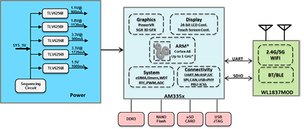
One of the fundamental challenges in any high-resolution signal-chain design is ensuring that the system noise floor is low enough for the analog-to-digital converter (ADC) to resolve your signals of interest. For example, if you chose the TI ADS1261– a 24-bit low-noise delta-sigma ADC – you could resolve input signals as low as 6 nVRMS at 2.5 SPS and a gain of 128 V/V.

From a system perspective, however, it’s not just the ADC’s noise that you need to worry about: all components, including amplifiers, voltage references, clocks and power supplies, contribute some noise. What’s the cumulative effect of these devices on your system’s noise? And more importantly, will your system be able to resolve your signals of interest?

To help you better understand system noise and apply this knowledge to your designs, I recently wrote a technical article series called “Resolving the Signal.” The series examines common noise sources in a typical signal chain and complements this understanding with methods to mitigate noise and maintain high-precision measurements.

Here are the 10 most critical questions and answers from the series to get you started designing with precision ADCs,

 1.   What types of noise can you expect to find in ADCs?

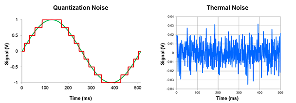
Total ADC noise has two main components: quantization noise and thermal noise. Quantization noise comes from the process of mapping an infinite number of analog voltages to a finite number of digital codes (the left side of Figure 1). As a result, any single digital output can correspond to several analog input voltages that may differ by as much as one-half least significant bit (LSB).

Thermal noise is a phenomenon inherent in all electrical components as a result of the physical movement of charge inside electrical conductors (the right side of Figure 1). Unfortunately, ADC end users cannot affect the device’s thermal noise because it is a function of the ADC’s design.

Figure 1: Quantization noise (left) and thermal noise (right)

Do thermal and quantization noise affect low- and high-resolution ADCs equally? Read part 1, “Introduction to Noise in Delta-Sigma ADCs,” to find out.

 2.  How is ADC noise measured and specified?

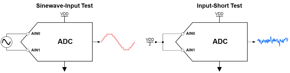
There are two methods ADC manufacturers use to measure ADC noise. The first method shorts the ADC’s inputs together to measure the slight variations in output code as a result of thermal noise. The second method involves inputting a sine wave with a specific amplitude and frequency (such as 1 VPP at 1 kHz) and reporting how the ADC quantizes the sine wave. Figure 2 demonstrates these types of noise measurements.

Figure 2: Sine-wave-input test setup (left) and input-short test setup (right)

Which ADCs use which type of measurement method? Read more about noise measurement methods and specifications in part 2.

 3.       What is the best noise parameter to use for system noise analysis?

For ADC noise analysis, I recommend using input-referred noise. I’ve bolded this phrase because it’s not common practice to use input-referred noise to define ADC performance. In fact, a majority of engineers speak exclusively in terms of relative parameters such as effective and noise-free resolution and are deeply concerned when they cannot maximize those values. After all, if you need to use a 24-bit ADC to achieve a 16-bit effective resolution, it feels like you’re paying for ADC performance you won’t actually use.

However, an effective resolution of 16 bits doesn’t necessarily tell you anything about how much of the full-scale range (FSR) your ADC will use. You may only need 16 bits of effective resolution, but if the minimum input signal is 50 nV, you will never be able to resolve that with a 16-bit ADC. Therefore, the true benefit of a high-resolution delta-sigma ADC is the low levels of input-referred noise it offers. It does not mean that effective resolution is unimportant – just that it is not the best way to parameterize a system.

Part 3 takes these claims one step further with a design example that uses both noise-free resolution and input-referred noise to define a system noise parameter. Which one enables the quickest, most adaptable solution? Read the article to discover the answer.

 4.       What is ENBW and why is it important?

In general signal-processing terms, a filter’s effective noise bandwidth (ENBW) is the cutoff frequency, fC, of an ideal brick-wall filter whose noise power is approximately equivalent to the noise power of the original filter, H(f).

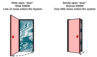
As an analogy, consider your home on a cold night. To reduce energy costs and save money, you need to keep your doors and windows closed as much as possible in order to limit the amount of cold air coming in. In this case, your home is the system, your doors and windows are the filter, the cold air is noise, and the ENBW is a measurement of how open (or closed) your doors and windows are. The larger the gap (ENBW), the more cold air (noise) gets into your home (system) and vice versa, as shown in Figure 3.


Figure 3: Wide ENBW leads to more noise (left); narrow ENBW leads to less noise (right)

What system components contribute to ENBW? Read part 4 to learn more.

  1. 1.       How do you calculate the noise bandwidth of your system?

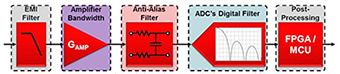
If your signal chain has multiple filter components, you must calculate the ENBW for each component by combining all downstream filters in the signal chain. To combine filters, plot them as magnitude (in decibels) vs. frequency and add them point by point.

For example, to calculate the noise contribution of the amplifier in Figure 4, you would have to combine the amplifier’s bandwidth with the anti-aliasing filter, the ADC’s digital filter and any post-processing filters. You could ignore the electromagnetic interference (EMI) filter in this case since it is upstream relative to the amplifier.


Figure 4: Typical signal chain showing multiple sources of filtering

Since this can be complicated, read part 5 to learn ENBW approximation methods to simplify your analysis.

 6.       If you add an external amplifier to the input of an ADC, how does this affect system noise performance?

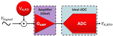
You can make your noise analysis easier by separating both the ADC and amplifier from their respective noise sources. In this case, you can model your system as a noiseless amplifier and noiseless ADC preceded by a voltage source equal to the input-referred noise of both, as in Figure 5.

Figure 5: “Noiseless” ADC and amplifier preceded by total noise, referred-to-input

Unfortunately, the measured output noise must refer back to the input, since input-referred noise is the specification used in most ADC data sheets. Assuming that the amplifier and ADC noise are uncorrelated, take the root-sum-square (RSS) of both values to determine the total output-referred noise. You also need to scale the amplifier noise by the amplifier’s gain, GAMP. Equation 1 shows the resulting output-referred noise:


How do you translate this to input-referred noise? And what are the ramifications of the gain scaling factor, GAMP? Read part 6 to find out.

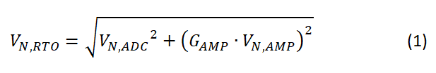
 7.       Is there such a thing as too much gain?

In the seventh series installment, I looked at an example that added multiple external amplifiers to the input of the ADS1261 and measured the resulting noise performance. I then compared these combinations to the ADS1261’s baseline noise performance using its integrated programmable gain amplifier. To make the comparison easier, I plotted the noise at different gain settings for each combination, which offers several insights about how adding external amplifiers to precision ADCs affects performance, as well as how performance changes with gain. Figure 6 depicts the plot.

Figure 6: Comparing noise performance of different amplifiers plus the ADS1261 as a function of gain

What are the key takeaways from this example and the plot in Figure 6? Read part 7, “The Effects of Amplifier Noise on Delta-Sigma ADCs,” to learn more.

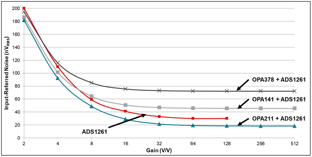
 8.       How do you calculate the amount of reference noise passing into your system?

One of the most interesting characteristics of reference noise is that it changes linearly with how much of the ADC’s FSR that you use. If you have a very small input signal, you won’t see much reference noise – and can potentially use a noisier reference as a result. Or if your input signals are greater than mid-scale, you can expect the reference noise to dominate. In this case, always make sure that the ADC noise and reference noise are comparable. Figure 7 qualitatively plots reference noise, ADC noise and total noise as a function of FSR utilization.

Figure 7: Reference noise, ADC noise and total noise as a function of FSR utilization

What do the key points – A, B and C – on this plot represent? And how does changing your input signal vs. changing your system gain affect reference noise? Find the answers to these questions in part 8.

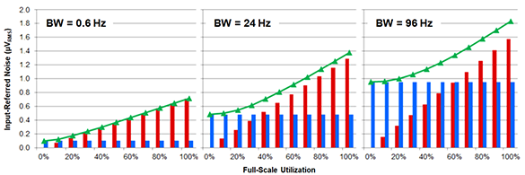
 9.       How can you reduce the amount of reference noise passing into your system?

One common way to reduce the amount of reference noise passed into the system is to limit the system’s overall ENBW. This can be achieved by slowing down the ADC’s output data rate. Figure 8 shows how reducing the ADC’s output data rate decreases both ADC noise and reference noise simultaneously. For example, between ENBW = 0.6 Hz (left) and ENBW = 96 Hz (right), the reference noise at 100% utilization decreases by a factor of 2.3, while the ADC noise decreases by a factor of 10, resulting in far less total noise.

Figure 8: Limiting ENBW reduces total noise: 0.6 Hz (left), 24 Hz (middle), 96 Hz (right)

Read part 9 to learn about how your reference configuration can also reduce the amount of reference noise passing into your system.


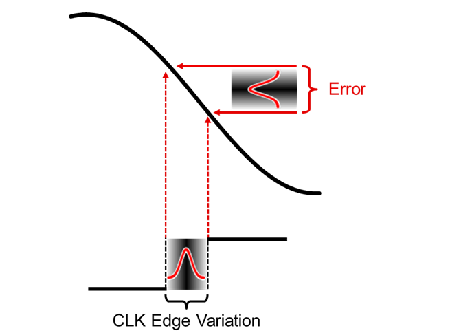
  1. 1.       Can clocks affect your ADC’s noise performance?

Although you may expect an ADC’s sampling period to be perfectly constant, there is always some deviation from the ideal. “Clock jitter” refers to the variation in a clock waveform’s edges from one period to the next. Since all ADCs use a clock edge to control the sampling point, clock-edge variation creates deviations in the sampling instance. This deviation results in a non-constant sampling frequency that appears in the conversion result as another source of noise. Figure 9 shows the sampling-edge variation caused by clock jitter on a sinusoidal input signal.


Figure 9: Clock signal showing sampling-edge variation caused by jitter

To learn how clocks cause additional errors, as well as ways to reduce system noise due to clocking, read part 10.

While these are some of the most important questions answered in the “Resolving the Signal” series, I covered many more topics and examples to help you get the best noise performance out of your high-resolution, delta-sigma ADC signal chain. Read the series to learn more, and if you have any additional questions, feel free to post them in the comments below.

Voltage supervisor requirements for e-meter applications

$
0
0

Introduction

As the electricity grid around the world becomes smarter over time, complex electronic designs are necessary. At the same time, long-term system reliability cannot be compromised. A smart e-meter monitors various system voltages to prevent unexpected conditions that cause inconsistent measurements or system failures.


The generic e-meter application shown in Figure 1 consists of several blocks that work together to measure consumed electricity.

  Figure 1: E-meter system block diagram example


This post explains the purpose of the DC/DC power supply, metrology and applications blocks (outlined in red) and dives deep into the importance of the supply voltage supervisor/watchdog timer subsystem. From a general design perspective, a system that monitors electricity consumption needs to be precise, compact and reliable.


DC/DC power supply subsystem requirements: wide VIN and low IQ

An e-meter typically receives 12 V to 24 V from the main AC power supply before converting it into a 3.3-V or 5-V DC voltage to power the rest of the system. A voltage supervisor ensures that the main power supply and all power rails are within the system requirements so that the system operates correctly. If the voltage in this block fails or browns out, the voltage monitoring solution needs to flag the fault condition so that the rest of the system can shut down properly.


If the main power supply does not provide enough power, a switch will connect a backup battery or supercapacitor into the system to provide the required power temporarily. In general, systems that rely on backup power reserves can benefit from any power savings in such critical operating conditions, since lower-power systems will last longer on the power reserves. The DC/DC power-supply block requires a voltage supervisor that has a wide VIN to monitor up to 24 V, and low power when using the power reserves.


Metrology and applications subsystem requirements: high accuracy and programmable delay

The metrology block connects to the outside world through sensors, and is responsible for the actual electricity measurements before sending the information to a microcontroller (MCU) for processing. The applications block has another MCU that formats and stores data in addition to displaying information. This block is responsible for monitoring the whole system and serves as the main interface between the system and the data output.


Accurately monitoring the voltage rails powering the MCUs and MCU activity is critical in these blocks to ensure reliable and consistent measurements. If the MCU is not in the correct operating condition, a voltage supervisor or watchdog timer can flag a fault before any other issues arise. When monitoring a voltage, specifically in a system that requires precise, robust and reliable measurements, voltage monitoring accuracy is important to determine quickly and exactly when the system is not functioning at optimal performance.


Additionally, whenever an application uses an MCU or several different peripherals, there may be the need for programmable startup delay for sequencing purposes. Programmable delay serves an important function when the MCU or other peripherals need a specific amount of time to boot up or to accomplish a task before the system can begin functioning normally. Also, when a fault condition occurs, there may be a need for a specific reset delay for the MCU and/or peripherals to accomplish a task before releasing the reset. In this case, the programmable delay feature provides a programmable and simple solution to add flexibility.


Review of e-meter design requirements

All three of the blocks outlined in Figure 1 require voltage supervisors with a wide VIN, low power, high accuracy and programmable delay. A good option to consider is the TPS3840, as it offers a balance of these requirements in one device.


The TPS3840 has a wide input voltage range up to 24 V or higher with external resistors for monitoring the high- and low-voltage rails, 1% typical voltage monitoring accuracy, and only consumes 350 nA of power while offering programmable delay. In addition, the TPS3840 provides significant precision and flexibility that is not obtainable with internal analog-to-digital converter monitoring in the MCU alone. Compared to the internal ADC monitoring in the MCU, the TPS3840 has more flexibility in the voltage monitor threshold options, a lower power-on-reset voltage and a quicker startup delay.


Power-on reset is defined as the minimum input voltage before the output becomes defined, which is essential for preventing glitches that can produce false faults or premature system startup. The startup delay for the TPS3840 is only 220 µs, meaning that the TPS3840 can begin monitoring voltage before the rest of the system even powers up. Overall, voltage supervisors ensure proper system functionality by continuously monitoring the voltage rails going in to power the internals of an e-meter.


An external watchdog timer in both the metrology and applications blocks will ensure that the MCU does not latch or glitch periodically by detecting pulses sent by the MCU’s general-purpose input/output pin. If the software glitches and a pulse is missed, the external watchdog timer will reset the MCU.


The TPS3430 programmable watchdog timer is a good option since it offers programmable watchdog timeout and watchdog reset delay to meet the timing requirements of any MCU. If you need both a voltage supervisor and watchdog feature, TI has many devices that fit this need. Review the “Voltage Supervisors Quick Reference Guide under the Supervisor + Watchdog Timer heading for all options.


Additional resources

How a small SOT563 DC/DC converter supplies multirail power in industrial applications

$
0
0

Hardware design engineers are forever looking for new solutions for their design tasks. But they are also under time constraints to solve all of the challenges of a new project: always smaller, always more functionality, always lower cost, and with a reliable, well-engineered and tested board.

More and more supply rails are required for power supplies in industrial programmable logic controller (PLC) systems with central processing units, input/output and communication modules, or human machine interface (HMI) panels. Board space is running out quickly.

Small-outline transistor SOT23 is a common package type for DC/DC converters in such applications; however, it consumes a relatively large amount of area on the board. With more than 8 mm2 of package and inductors at 4 mm by 4 mm or larger, the available board space in an industrial system is limiting the number of power rails that you can implement. Moving to an ultra-fine-pitch ball-grid array or chip-scale package is often cost-prohibitive in mass production, and comes with soldering and bench-testing challenges.

SOT563 combines the advantages of a leaded package with a very small size (Figure 1). It is not a new package for semiconductors. Available for several years for discrete components like metal-oxide semiconductor field-effect transistors, diodes or temperature sensors, it is now also available for DC/DC converters. The SOT563 package is 65% smaller than the ubiquitous SOT23 while still offering leads (pins) accessible to a probe (tester). In addition, these leads enable the use of low-cost mass-production facilities with visual inspection instead of the more complex X-ray checking of the soldering.

Figure 1: TI’s 3-A-output TLV62585DRL in the SOT563 DC/DC converter package

The SOT563 package’s small solution size makes it a good fit for multirail power supplies in HMI or PLC systems. You can place the voltage rails onto the board where they are needed, close to the loads for best performance and maximum flexibility. Instead of a single large power-management integrated circuit, a multiple-rail approach can simplify the board layout to a great extent and help optimize your system’s electromagnetic interference performance.

The 12-mm-by-12-mm, 5-Rail Power Sequencing for Application Processors Reference Design, featuring the AM3358 Arm® Cortex® microcontroller, is an example of such an approach (Figure 2). As the title indicates, the total power solution size for the reference design’s five rails, including all required external components like inductors, capacitors and resistors, is just 12 mm by 12 mm.

Figure 2: 12-mm-by-12-mm five-rail power sequencing reference design using SOT563 buck converters

The power consumption of PLC modules is relatively low, typically not exceeding 2 W per module; most power-supply rails are therefore only up to 1 A, 2 A or 3 A. However, thermal constraints often prevent the use of linear regulators and therefore require a high-efficiency DC/DC converter for the point of load, like the new pin-compatible TLV62568/TLV62569/TLV62585 family (Table 1).

 Table 1: TI DC/DC converters available in the SOT563 package

The SOT563 package for DC/DC converters offers many advantages in terms of solution size and ease of use. It is quickly becoming the new standard package for many industrial applications, including those with HMIs and PLCs.

Additional resources

Read these blog posts:

Download the Small Efficient Flexible Power Supply Reference Design for NXP iMX7 Series Application Processors.

Learn more about power management for FPGAs and processors.

Watch the video, “How to meet an FPGA’s DC voltage accuracy and AC load transient specification.

Smart robots coming soon to a cubicle or kitchen near you

$
0
0


Robotics expert Matthieu Chevrier paints a picture of a future when industrial, domestic and professional robots collaborate with humans as part of daily life.

Not too long from now, a smart robot might be in your kitchen.

Imagine this: As you start your day, you greet the security bot that has monitored your home all night through its distributed mesh network of sensors. It switches your home to your preferred settings – window shades up, morning news on low, coffee ground and brewed, security alarm off.

Your smartphone alerts you that a courier robot is making its way down the road to deliver refills of razors and toothpaste to your front porch. You step around the cleaning bot making its morning rounds.

At work, a collaborative robot has tested and prepared a prototype for a big client meeting. With a smile and a handshake, you secure a major new order, and employees immediately put their own collaborative logistics, warehouse and manufacturing robots into action.

When you return home, the evening news captivates you with a story about fully autonomous, foldable drones that have squeezed through a narrow cave opening, located trapped spelunkers and then led a rescue team to their location.

It may seem like science fiction, but those of us steeped in the world of robotics and automation software know this future isn't far away – and will be built with technology that exists today.


 Read our whitepaper: How sensor data is powering AI in robotics

A dramatic shift in human-machine roles

From my perspective as a system and applications engineering manager who spends every day thinking about robots, the trends and market drivers are clear. We’re in a period of transition: The roles of humans and machine in our work and personal lives are shifting dramatically.

Many robots, including delivery drones and automated logistics robots, are already in development. Thirty-three million domestic and professional service robots – those outside industrial settings that perform tasks for humans – are projected to sell between 2018 and 2020, according to The International Federation of Robotics, and we expect a similar surge in hospitality robots. Industry experts predict they'll enter into many parts of our lives where none exist now, including robots that:

  • Check us into a hotel and bring us room service
  • Guide us to an item we can't find in the supermarket
  • Deliver packages to our mailbox
  • Cut our lawns and tend our gardens and homes
  • Assist doctors and hospital staff in medical procedures
  • Lead us to our departure gate at the airport


What’s powering collaborative, adaptable and highly mobile robots

Much like a human’s five senses relay information to the brain, next-generation robotics rely on the fusion of sensor data and machine learning to make real-time decisions and navigate dynamic real-world environments.

Humans do this intuitively, using our eyes and ears together to understand when someone is talking to us, where that person is and which person in a group is doing the talking.

These components work together to give robots a better picture of the world than any one sensor alone, and they’re pushing the boundaries of technological capabilities and unleashing functionality that has never been possible.

Machines become surgical assistants with the help of servomotors that enable precise, controlled motion. Drones become rescue bots with time-of-flight optical sensors, LIDAR and ultrasonic sensors that work together to enable autonomous flight and collision avoidance. In tropical climates, industrial robots with temperature and humidity sensors become predictive maintenance powerhouses that anticipate dew points and protect electronic systems.

Sensors were once bulky and expensive, but an increasing number of them are being designed to be smaller, lower cost and faster to produce. Hardware and software technologies that bring algorithmic data processing out of the cloud and into the machine, like intelligent mmWave sensors, help eliminate the lag between sensing and responding.

This allows collaborative, adaptable and highly mobile robots to join and replace older machines that must be isolated from people and given simple, repetitive tasks.

Giving us quality time back

Since ancient times, we've sought ways that machines can give us an upper hand against nature and produce goods for our security and comfort. At work, the value of replacing pickaxes with steam shovels and mule teams with farm equipment is obvious. Robotic arms were introduced in the 1950s to handle tasks such as welding car parts or moving heavy components. At home, vacuum cleaners and washing machines drastically reduced the time required for household chores in the 20th century.

Today, developers are building machine learning and sensors into robots so they can intelligently work shoulder-to-shoulder with humans and respond to changing conditions. In our personal lives, the same sensors and intelligence are reducing the time and attention we need to spend on daily chores. Think about it: We do so many things today because we must do them -- not because they bring joy or meaning to our lives.

As robots gain autonomy around our homes, streets and workplaces, much of the time we spend being neither productive nor creative because of our chores will be given back to us. The time we dedicate to basics like transportation, household maintenance and repetitive tasks will diminish significantly.

As the robot in your office delivers your documents or allows you to have a virtual presence in a meeting room, you can spend more time doing high-value work, planning that next big breakthrough, or being with family and friends.

The technology is here. How far we’ll go with it is yet to be seen.

Matthieu Chevrier is system and application manager for robotics and programmable logic controllers at our company.

The problem with short-to-VBUS protection integrated into your USB Type-C™/USB Power Delivery controller

$
0
0

Due to the smaller connector/receptacle size and reduced pin pitch, USB Type-C presents several new failure scenarios that can damage downstream circuitry. The most common failure scenario is mechanical twist; see Figure 1. Once a USB PD contract >5 V (such as 20 V, 15 V or 9 V) has been received by the USB PD Controller, if the USB plug is removed at an angle, it might causethe USB Type-C connector’s bus power lines (VBUS) to short with the adjacent pins – or more specifically the configuration channel (CC) and sideband use (SBU) lines.

Figure 1: Mechanical twist failure scenario

Why does this matter? Well, for most systems, the downstream circuitry (or USB Type-C/USB PD controller) is rated for only 6 V maximum on the CC/SBU pins. Engineers have two choices: add an external protection chip or select a USB Type-C/USB PD Controller with CC/SBU lines rated for 24 V or more. Let’s look into why forgoing the protection chip may not be the best idea.

External protection works because if there’s an electrostatic discharge (ESD) event or VBUS shorting on port No. 1, the protection chip opens series field-effect transistors – thus isolating the high voltage from the rest of the system. The chip also dissipates any residual energy (on both system and connector sides) through internal clamping diodes. Then, the protection device resets and protects the rest of the system.

Internal protection doesn’t work because in the case of an ESD event or VBUS short on Port No. 1, the USB PD controller resets itself, bringing down both port No. 1 and port No. 2 as seen in Figure 2. In addition, the USB PD controller runs the risk of having the configuration or flash corrupted during this high rate of voltage change (dv/dt) event. It could leave the system in a nondeterministic state with unknown general-purpose input/output values or even cause the microcontroller to lock up. Even worse, if the USB PD controller doesn’t have properly designed internal clamps to absorb the energy, the device itself could be damaged.

Figure 2: External protection offers fault isolation

These failures are easily avoidable by adding an external protection device such as the TPD6S300A. The TPD6S300A’s ability to clamp the voltage quickly and efficiently helps enable a robust and reliable solution for designers.

Additional resources


The hidden cost of optocouplers for isolated RS-485 designs

$
0
0

Optocouplers, also known as optoisolators or photocouplers, have been used to achieve galvanic isolation in electronic circuits for more than 40 years. Optocouplers use an LED and phototransistor to enable signal communication without the transfer of current. Historically, optocouplers have been popular because they were a low-cost solution. However, given the advancements in digital isolation technology, are optocouplers really the most cost-effective method to achieve galvanic isolation for an RS-485 system?

Figure 1 shows a typical circuit for isolating an RS-485 transceiver using optocouplers to achieve galvanic isolation. A total of three optocouplers are required in this solution: two high-speed optocouplers (one each for transmit and receive signals) and a low-speed optocoupler for direction control. This solution will also require a significant amount of external components, including Schmitt buffers, a Schmitt trigger, resistors and bypass capacitors. All of these components can add up both in cost and board area.


Figure 1: An isolated RS-485 design using optocouplers

Many system designers today across a variety of industrial markets are encountering issues with board-space constraints as they move toward smaller overall solution sizes or increased functionality with each new generation. One example of this is heating, ventilation and air-conditioning (HVAC) systems that regulate temperature and airflow in buildings. With the growing trend toward smart, energy-efficient buildings, new HVAC control boards need to be able to incorporate advanced monitoring and interface with smart thermostat systems without increasing the overall solution size.

  
Optimize your isolated RS-485 designs

 Learn more about how to replace optocouplers in your isolated RS-485 designs by reading our application note "isolate RS-485 for smallest size and highest reliability".


RS-485 is a common communication interface in these systems because of its reliability over long distances. When RS-485 nodes are placed at locations with different ground potentials, common-mode noise can cause communication errors, resulting in a need for isolation to prevent these ground-potential differences. Using a bulky optocoupler solution to isolate RS-485 can force designers to make compromises elsewhere in the system, driving the need for smaller isolated interface solutions.

In addition to the large solution size, many designers will also encounter these performance concerns with optocouplers:

  • Reliability. Optocouplers will typically use epoxy as their dielectric; epoxy will break down at lower voltages compared to other common dielectrics, shown in Figure 2. Assembly inconsistencies and LED degradation will also cause device-to-device variations in terms of isolation reliability and lifetime.

Figure 2: Dielectric strength of common insulator materials

  • Power consumption: Each optocoupler requires 5-10 mA to drive the LED on the internal input die.
  • Temperature range: Optocouplers are mostly limited to an 85°C maximum ambient temperature, with rare exceptions that are capable of as much as 105°C for a high premium.
  • Switching specifications: Rise/fall time and propagation delay in optocouplers can vary depending on the biasing current, current transfer ratio and device-to-device variation.
  • Noise immunity: Typical common-mode transient immunity for optocouplers ranges from 15 kV/µs to 25 kV/µs. In the presence of voltage transients above this level, data corruption is likely.

To meet the growing need for compact solutions without compromising performance, TI has created the ISO1500 isolated RS-485 transceiver. Figure 3 compares the solution size of the optocoupler solution shown in Figure 1, an industry-standard 16-pin small-outline integrated circuit (SOIC) isolated RS-485 transceiver and the ISO1500. Note that these designs only show the signal isolation of the RS-485 transceiver. The application note, “How to Isolate Signal and Power for an RS-485 System”, provides a helpful overview for isolating power in RS-485 systems.


Figure 3: Solution size comparison between the optocoupler solution (a); an industry-standard 16-pin SOIC isolated RS-485 transceiver (b); and TI’s ISO1500 (c)

The ISO1500 reduces board space by as much as 85% compared to the discrete optocoupler solution and as much as 50% compared to the industry-standard 16-pin SOIC package. In addition to minimizing solution size, the ISO1500 also solves many of the performance concerns that I mentioned above. All TI isolated RS-485 transceivers are created in a semiconductor fabrication process using silicon dioxide as the dielectric to minimize device-to-device variation and provide more reliable high-voltage performance. The ISO1500 consumes <10 µA of current to drive the complementary metal-oxide semiconductor-based inputs, can be used from -40°C to 125°C, has predictable switching specifications, and showcases much higher noise immunity compared to a traditional optocoupler. When you combine these system-level benefits with the board-space savings that come with using the ISO1500, it becomes clear that the cost of an optocoupler adds up to significantly more than the price paid for just the device.

Additional resources

This day in TI space: from 1958 to today

$
0
0
When we say that our space products are out of this world, we mean it. Our heritage in space exploration is rich, dating as far back as 1958 with the launch of the U.S.’s first satellite, Explorer I, several months before our very own Jack Kilby...(read more)

How to prevent battery over discharge by using a precise threshold voltage enable pin

$
0
0

Using a buck-boost converter is a convenient way to obtain a fixed supply voltage within the wide voltage range of typical batteries used in low-power devices such as smart meters, wearables or those in the Internet of Things. In order to extract as much energy as possible from the battery, it helps if the converter can operate at very low input voltages.

In buck-boost devices such as the TPS63802, the minimum operating input voltage is as low as 1.3 V once the device is started. With most rechargeable batteries, however, deep discharge can irreversibly damage the battery. In such situations, it becomes useful to have the option to cut off the battery supply at a desired value, say 2.5 V for a one-cell lithium-ion battery.

A typical DC/DC converter has an input pin to enable or disable the converter. However, the threshold voltage at this pin usually has a high tolerance, making it difficult to pinpoint the desired cutoff voltage. As an example, according to its data sheet, the threshold voltage of the enable (EN) pin for the TPS63020 is somewhere within the range listed in Table 1. 

Parameter

Min

Typ

Max

Unit

VIL

EN input low voltage


0.4

V

VIH

EN input high voltage

1.2


V

Table 1: EN pin threshold voltage for the TPS63020

This threshold range is fine for on/off control using logic-level signals, but not if you want to set a precise cutoff voltage derived from the input voltage. To achieve higher accuracy, it is possible to add a comparator and a voltage reference, but this increases complexity and cost.

My colleague Chris Glaser introduced the concept of achieving a precise threshold voltage for buck converters in his Analog Design Journal article, “Achieving a clean startup by using a DC/DC converter with a precise enable-pin threshold.” The new TPS63802 buck-boost converter also has very precise threshold voltage for the EN pin, with approximately 3% accuracy and 100-mV hysteresis, as listed in Table 2. 

Parameter

Min

Typ

Max

Unit

VTHR,EN

Rising threshold voltage for EN pin

1.07

1.1

1.13

V

VTHF,EN

Falling threshold voltage for EN pin

0.97

1

1.03

V

Table 2: EN pin threshold voltage for the TPS63802

It is possible to easily set a user-defined minimum supply voltage with a voltage divider, as shown in Figure 1.

 Figure 1: Setting the input cutoff voltage with a voltage divider

Equation 1 expresses the falling threshold supply voltage when the converter is turned off as:


Equation 2 calculates the rising threshold supply voltage when the converter is turned on:


The additional voltage divider will increase the current consumption; therefore, aim for large resistances. However, considering that the EN input leakage current is 0.2 μA maximum, aim for at least 20 μA of current in the voltage divider. The application report, “Optimizing Resistor Dividers at a Comparator Input,” has more details about how to optimize a resistor divider at a comparator input.

As an example, to set the cutoff input voltage to VTHF,IN = 2.5 V, first choose R1 + R2 = 125 kΩ to have a 20-μA resistor divider current. Solving Equation 1, choose R1 = 75 kΩ and R2 = 49.9 kΩ resistors with 1% tolerance. The turn-on input voltage is now VTHF,IN = 2.75 V according to Equation 2.

Figure 2 shows that the achieved cutoff and turn-on input voltages are 2.56 V and 2.8 V, respectively. This is within the equivalent 6σ tolerance of approximately 80 mV (3.1%) caused by the EN pin threshold voltage and resistor tolerances, not taking into account oscilloscope accuracy. The application report, “AN-1378 Method for Calculating Output Voltage Tolerances in Adjustable Regulators,” has more details on calculating equivalent voltage tolerances.

Figure 2: Achieved cutoff and turn-on input voltage thresholds

Conclusion

The previous example showed how you can easily protect your battery from overdischarge by adding only 2 resistors. The same solution is applicable not only to buck-boost but also to other buck or boost devices with a precise EN pin threshold voltage.

If you have any questions about TI buck-boost devices, see the TI E2E™ Community Power Management forum.

Intelligence at the edge powers autonomous factories

$
0
0
A variety of robots, from traditional industrial robotic systems to today’s latest collaborative robots, rely on sensors that generate and process large volumes of highly varied data. This data can be used to enable autonomous robots that can make...(read more)

“The Jetsons” are coming to an electric vehicle near you – sort of

$
0
0

“The Jetsons” cartoon, which aired on television in the early 1960s (and again with new episodes in the 1980s) featured a family in the year 2062 riding around in a flying car. While we don’t have flying cars yet, we are soon going to hear similar sounds from the electrified vehicles (EVs) around us.

There are three main types of EVs:

  • A hybrid electric vehicle (HEV) uses a combination of electric motors and a standard internal combustion engine.
  • A plug-in hybrid electric vehicle is a variant of the HEV. It still has a standard internal combustion engine and electric motors, but the internal battery can be recharged by plugging it into an external source of electric power.
  • A battery electric vehicle is a motorized vehicle that solely uses electric motors for propulsion.

It’s well-known that EVs produce very little engine noise compared to traditional internal combustion engines, thereby posing a risk for the blind, small children, the elderly, runners, cyclists or any pedestrians who need to hear that a vehicle is approaching. One study shows that these quieter EVs are 40% more likely to collide with pedestrians than cars with a regular combustion engine. Another study indicated that a pedestrian may not adequately hear EVs traveling at slow speeds until they are just 1-2 seconds away from impact – often too late to avoid harm.

Several factors contribute to the reason why EVs are quieter: They make no noise when starting up, and they make no appreciable noise taking off from a stop sign or stoplight or when driving in reverse.

I can confirm this experience, since I recently went shopping for a new family car. On an HEV, for instance, you simply push a button to start the car, but you don’t hear the familiar sound of the starter cranking over to start the combustion engine.

You just get a green indicator light that says “ready.” You have to get used to how quiet the car is, since there is no familiar engine sound.

Once you start driving, you begin to realize that whether you’re going in reverse or moving forward, you still don’t hear the combustion engine start up until you hit approximately 20 mph.

In addition, the car shuts off the combustion engine automatically at some stopping points to conserve fuel. This means that when you start taking off again from a stop sign or traffic light, the vehicle is completely silent until it reaches an appropriate speed, at which point tire and wind noise can become significant.

It’s precisely for these reasons that governments are starting to mandate the installation of devices on EVs that will emit an external sound when traveling at low speeds to alert pedestrians to the car’s proximity and help avert potential accidents; see Figure 1. Depending on the region of the world, these devices are called virtual engine sound systems (VESS), acoustic vehicle alerting systems (AVAS) or engine/vehicle sound generators.

Figure 1: Scenarios that can benefit from VESS

The new governmental requirements generally stipulate that a VESS must emit sound when the EV is operating in reverse and while the vehicle is in forward motion up to a maximum defined speed (in the U.S., 30 kph; in Europe, 20 kph).

The sound pressure level of the emitted sound must vary by a specified amount as the vehicle’s speed increases or decreases in order to alert pedestrians to its changing speed.

VESS regulations typically do not mandate the exact type of tone/signal that needs to be emitted, but some of the early prototypes vary the tone/pitch to give the acoustic impression of an approaching spaceship – hence my reference to “The Jetsons.” Current implementations seem to be targeting tones that are somewhat futuristic sounding, but also harmonious, as you can hear in Figure 2.

(Please visit the site to view this audio)

Figure 2: TI simulation of a harmonious VESS sound

In some cases, car manufacturers are also choosing to implement an additional speaker in their VESS implementation at the rear of the car, to provide an additional safety measure by adding an extra tone to signal that the car is reversing and to allow for a more aesthetically pleasing/natural sound impression around the entire vehicle. The sound may even taper off toward the rear of the vehicle if the design only implements a front speaker.

Because VESS regulations are still evolving globally, automotive audio amplifier manufacturers are rapidly moving to assure that their amplifier portfolios will support this newly emerging automotive end-equipment market space. Many car manufacturers are looking for a scalable automotive audio amplifier solution that can allow them to achieve lower R&D costs by simply building one board design to satisfy either front-speaker-only VESS designs or implementations requiring both front and rear VESS speakers.

Texas Instruments (TI) offers a scalable family of Class-D automotive audio amplifiers that meets VESS market demands. TI is the only automotive audio amplifier manufacturer to offer a two-channel, digital input, Class-D automotive qualified amplifier – the TAS6422-Q1. TI also offers compatible one- and four-channel Class-D automotive audio amplifiers that provide the scalability and flexibility car manufacturers need to address the VESS market.

Additional resources

Anything but discrete: How to simplify 48V to 60V DC fed three-phase inverter design

$
0
0
Imagine that you’re designing the next power stage of a servo, computer numerical control (CNC) or robotics application. In this instance, the power stage is a low-voltage DC-fed three-phase inverter for voltages ranging from 12 V DC to 60 V DC...(read more)

Top 7 design questions about digital isolators

$
0
0

Looking for more information about digital isolators? We’re here to help. Based on TI E2E™ Community feedback, we compiled a list of the most frequently asked questions about digital isolator design challenges. We hope this list will provide useful insights when isolating signals and power.

1. What is the difference between basic and reinforced digital isolators?

Basic digital isolators have to pass a suite of tests according to component-level standards such as Deutsches Institut für Normung (DIN) V Verband der Elektrotechnik, Elektronik und Informationstechnik (VDE) V 0884-11. DIN V VDE V 0884-11 defines the voltage levels that the isolator can withstand, such as the maximum surge isolation voltage, VIOSM; the maximum transient isolation voltage, VOITM; and maximum repetitive peak isolation voltage, VIORM (as explained in the white paper, “High-voltage reinforced isolation: Definitions and test methodologies”). Reinforced digital isolators, in addition to passing these tests, have to pass a minimum surge voltage test level of 10,000 VPK.

2. Can you power the two sides of a digital isolator with different voltages?

Yes. Digital isolators can be supplied voltages within the recommended operating conditions on both sides of the device. Since an isolation barrier separates the two sides, each side can be sourced independently with any voltage within recommended operating conditions. For example, it’s possible to supply ISO7721 VCC1 with 3.3 V (which is within 2.25 V to 5.5 V) and VCC2 with 5 V (which is also within 2.25 V to 5.5 V). This way, you can use the digital isolator as a logic-level translator in addition to providing isolation. The two sides of the isolator are independent.

3. Can a digital isolator signal voltage be different from its power-supply voltage?

No. The input/output signal voltages of digital isolators depend on its applied power-supply voltage. Hence, for the digital isolator to be compatible with the devices it interfaces to, it’s best to keep signal voltages similar to the isolator power-supply voltage. For example, when the ISO7721 is powered with 5 V and interfaces to a microcontroller (MCU), it is important that the MCU signals are also operating at 5-V logic levels.

4. What is the logic state of a digital isolator with no input signal?

When the input channel of a digital isolator is unpowered or the pins left floating, its respective output pin takes a predefined state (called the default state or fail-safe state), which can be either low or high depending on the device chosen. The suffix “F” in a device part number indicates the default state of output channels of the isolator. For example, no F in the ISO7721DWR indicates that the default state for this device is high. Similarly, the F in the ISO7721FDWR indicates that the default state for this device is low.

5. Can you leave unused channel pins on a digital isolator floating?

No. Input pins of unused channels of a digital isolator can be left floating for testing purposes, but in applications, leaving the unused pins floating could make the product less immune to noise.

The floating pins are especially prone to noise pickup when the system is subjected to electromagnetic compatibility (EMC)/immunity tests. To make the system immune to such noise, it is best to tie the channel inputs to their respective default logic states.

For example, for the ISO7721DWR, it is best to connect the unused signal input pin to its VCC through a pull-up resistor (preferably with a 4.7-kΩ resistance). For the TI ISO7721FDWR, it’s best to connect the unused signal input pin to its GND pin and leave. For both devices, the output pins of all unused channels are best left unconnected.

6. How can you determine the power consumption of a digital isolator?

You can calculate the power consumption of a digital isolator from specifications listed in their data sheet. Locate the Supply Current Characteristics table for your corresponding supply voltage (2.5 V, 3.3 V, 5 V). Within this table, find the data rate closest to the speed of your application signals. The data sheet will list the current consumption for that particular data rate, as a separate total for each side of the isolation barrier (ICC1 and ICC2). Adding these two currents together gives you the total current consumption of the device under that operating condition. Dividing it by the channel count of the digital isolator gives you the per-channel current consumption. Some data sheets also provide this total supply current per channel separately. For example, the ISO7041 data sheet shows a typical current consumption of 4.2 µA under the Total Supply Current Per Channel parameter, which is the ICC1(ch) plus ICC2(ch) currents.

7. How do you generate isolated power for a digital isolator?

There are several options to generate isolated power for a digital isolator; the best solution depends on the specific application needs.

One option is to use a transformer driver like TI’s SN6501, which operates in a push-pull configuration with a transformer and optional rectifying low-dropout regulator on the secondary side (Figure 1). The SN6501 is capable of delivering as much as 1.5 W to provide isolated power. This device has the flexibility for use in almost all applications because the transformer and turns ratio can provide the necessary isolation rating and output voltage for the power supply. You can use the SN6505x instead of the SN6501 for as much as 5 W of output power if you need isolated power for additional devices. The SN6505 has extra protection features such as overload and short circuit, thermal shutdown, soft start, and slew-rate control, enabling a robust solution.

Figure 1: Isolated power for the ISO7741 using the SN6501

Another option for space-constrained applications is the ISOW78xx family of devices, including the ISOW7841, which provides signal and power isolation in a 16-pin small-outline integrated circuit package. This combination, as featured in Figure 2, is compact, doesn’t require a transformer and makes certifications easy.

Figure 2: Digital isolator with integrated signal and power using the ISOW7841

What questions did we miss?

If you’re looking for more information about digital isolators or have a question you would like to see added to this list, leave a comment below and help us keep the conversation going.

Additional resources


Output topology options for a voltage supervisor

$
0
0

 Having stumbled upon this blog post, I’m assuming that you know the importance of having a voltage supervisor in your electronic design and are wondering how to implement and design with these different output topology types. Don’t worry! You came to the right post. But before I explain the different output topologies, I want to reiterate the importance of having a voltage supervisor, as many engineers are not familiar with this device.

Given the variable amounts of load that a system can have, the power supply is not always clean and can bounce around its typical output value. With this bounce in power supply, a device known as a voltage supervisor can provide protection from accidental surges or falling power, and improve the efficiency of electronic devices. This makes voltage supervisors a requirement in any electronic application.

The voltage supervisor products available on the market distinguish themselves by features such as threshold selections, multichannel monitoring options, detection accuracy, output configurations, fixed or adjustable delay, and watchdog features. In this post, I’ll focus on the different output configurations and review what you should consider when designing with these output topologies.

Output configurations

Think of a supervisor as an analog-to-digital converter. It senses a supply voltage (analog) and provides a flag (either the RESET or SENSEOUT pin), which is a digital signal. The digital signal output can be in either an open-drain or push-pull topology.

The open-drain output topology

Here are some things to consider when designing with the open-drain output topology:

  • Open-drain outputs provide flexibility because they can pull up to any voltage (within absolute maximum) to comply with the logic of the load, rather than pulling the output up to the supervisor’s supply voltage or sense voltage. A pull-up resistor properly limits the current and maintains the low-level output voltage (VOL) and high-level output voltage (VOH) specifications.

  • It’s possible to wire-OR together multiple open-drain outputs through a single pull-up resistor. The open-drain output can also pull up to any voltage that complies with the logic of the load giving flexibility to a designer.

  • The pull-up resistance cannot be too low such that the current through the open drain damages the supervisor. When the internal n-channel metal-oxide semiconductor (NMOS) (Figure 1) is on, current from the pull-up resistor will go through the NMOS and be pulled to ground. You should select the pull-up resistance based on two criteria. The first criteria is the supervisor’s recommended maximum reset or sense current, called IRESET or ISENSE, which is specified in the data sheet. If the current being pulled to ground is higher than IRESET, the supervisor’s internal NMOS could be damaged. The second criteria is based on the VOL requirements of the load that the output of the voltage supervisor connects to. Lower pull-up resistors will also result in higher VOL due to the increase in reset/sense current.

  • The pull-up resistance cannot be too high such that the leakage current through the open-drain resistor at high temperatures falls outside the VOHspecification found in the data sheet. By increasing the pull-up resistance, VOH decreases due to the smaller reset or sense current, causing a smaller voltage drop across the internal metal-oxide semiconductor field-effect transistor (MOSFET).

  • The output rise time is decided by the pull-up resistance and the output board parasitic capacitance. For faster rise times, use smaller pull-up resistances.

  • The supervisor’s quiescent current (Iq) does not include the current through the pull-up resistor. If the pull-up voltage is pulled from the supply, the total system Iq will increase, as supply current will also go through the pull-up resistor. If the pull-up voltage connects to another source, the system Iq will equal the supervisor Iq from the data sheet. Since the pull-up voltage can connect to different supplies, the Iq specification of the supervisor does not account for the additional output current resulting from the use of a common supply.

  • An open-drain output configuration requires an additional component, a pull-up resistor, connected from the output to a power supply. Without the pull-up resistor, the outputs are undefined when the internal NMOS turns off, as there will be no power supply to pull from.

  • The open-drain output can change with the output pull-up supply, and any transient coupling will depend on the pull-up resistance used. A higher pull-up resistance can minimize the effects of transients from the output pull-up supply.

Figure 1: The open-drain output uses an internal N-MOSFET

The push-pull topology

Here are some things to consider when designing with the push-pull output topology:

  • The output of a push-pull configuration toggles between the supervisor’s supply voltage and ground, with no external pull-up resistance required. Notice how the output in Figure 2 does not use a resistor like in Figure 1, and how Vpullup is not present in Figure 2. Vdd and ground are toggled via the 2 MOSFETS.

  • The voltage at the output of a push-pull configuration can never go beyond the supervisor’s voltage supply by more than 0.3V, because the body diodes can turn on and damage the device. The body diode will take excessive current in forward bias mode.

  • The quiescent current of the supervisor accounts for the current through the external resistors that can be connected at the output of the supervisor.

  • It’s not possible to wire-OR together push-pull outputs like with the open-drain output topology.

  • Push-pull outputs are a good fit for high-speed applications because the push-pull output does not have the additional delay that the pull-up resistor causes in the open-drain topology.

Figure 2: In the push-pull output topology, a p-channel MOS (PMOS) and NMOS connect together, similar to an inverter

How to identify active low and active high

Different types of supervisors monitor under and overvoltage conditions and provide RESET/FLAG/POWERGOOD/SENSEOUT in an active-low or active-high output topology. “SENSEOUT” and “POWERGOOD” labeled pins are active when the supervisor senses the supply voltage is in normal operating condition, whereas a “RESET” labeled pin is active when the supervisor senses the supply voltage is in a fault (under- or overvoltage) condition.

An overvoltage active-high supervisor means that whenever the supply crosses VIT+, signaling an overvoltage condition, RESET activates to logic high.

Table 1 can help you identify the different supervisors.

Table 1: Active-high vs. Active-low supervisors.

Now that you know more about the different output topologies, you are one step closer to selecting the correct supervisor for your system. Check out TI’s quick search tool to help you find one.

Additional resources

The ins and outs of automotive rear-lighting design

$
0
0

Imagine driving in the early 1900s. Drivers relied on hand signals and shouts, plus a little bit of guesswork, to predict the actions of other cars on the road.

Thanks to modern rear-lighting solutions, drivers can better predict the actions of other drivers in all environments, making driving safer. We’ve advanced from kerosene lamps to incandescent light bulbs to the more reliable and efficient LEDs and organic LEDs. As technologies advance, so too have the number of light sources in vehicles – from a single bulb to multiple pixelated designs. Figure 1 offers some examples.

Figure 1: Components of a rear-lighting system

As rear-lighting systems become more complex, designers must consider a number of design challenges, from power and thermal management to electromagnetic interference compatibility to fault detection and protection.

I recently wrote a white paper, LED drivers in automotive rear lighting, that discusses solutions to these challenges, as well as trends and topologies to consider in your next design.

With the continued evolution of these systems, we can make the road a safer place for drivers and pedestrians alike.

Additional resources

Power-supply supervision circuits made simpler with DACs

$
0
0

When designers are defining a system-level power supply, one key consideration has to be the addition of the appropriate protection circuits in order to ensure that the design is not only effective, but robust. Although achieving system-level voltage and current protection can add complexity to your design, you can attain a solution with minimal compromise and cost by incorporating small, cost-effective digital-to-analog converters (DACs) plus simple window comparators.

TI’s 10-bit DAC53608 precision DAC, first in a new family of small, cost-effective voltage output DACs, offers just such a solution to this design challenge.

Power-supply supervision is a circuit required in almost all power-supply applications that use shared supply rails across multiple boards or modules. This circuit, while necessary for the protection of system-level components in case of a fault, is often perceived as adding design complexity and cost. Therefore, implementing a robust power-supply supervision circuit cost-effectively becomes one of the key challenges for any designer. Common applications requiring such supervision circuits include communications equipment, battery test systems and automated test equipment.

In this post, I will discuss the easiest methods for implementing an effective power-supply supervision circuit using the DAC53608.


Start your next design with an easy-to-use platform

 Quickly and easily demonstrate the functionality and versatility of the 10-bit, 12C interface, buffered-voltage-output DAC53608 with the evaluation module. Learn more.

Figure 1 provides a simple high-level view of how to implement power-supply voltage or current supervision. Simply put, each precision DAC sets a threshold for each window comparator, which is compared against the measured voltage or current. The comparator can then trigger the system processor in case the measured value moves outside the programmed band. For brevity, I’ll concentrate on voltage supervisors, since it’s possible to implement a current supervisor in a similar way.

Figure 1: Block diagram of power-supply supervision

Figure 1: Block diagram of power-supply supervision

One common approach to implementing power-supply supervision is to detect the direction of a failure inside a control loop in order to properly regulate the power-supply source. Let’s illustrate this simple design based using the DAC53608 10-bit DAC and TLV1701 dual comparator. This design requires two trigger outputs from every supervisory circuit, as shown in Figure 2. Two DAC channels independently generate the high and low threshold voltages. Resistors RA and RB bring the nominal value of the monitored voltage (VIN) into the range of the DAC. Using open-drain comparators is preferable here in order to generate trigger signals at the input/output voltage level of the processing circuit. When the attenuated input voltage increases beyond VTH-HI, the output VALARM-HI goes low. Similarly, VALARM-LO goes low when the attenuated output voltage decreases below VTH-LO; otherwise the outputs are pulled high. Figure 3 shows the waveforms generated at different nodes of this circuit.


Figure 2: Window comparator for a control loop

Figure 2: Window comparator for a control loop

Figure 3: Dual-output waveform

Figure 3: Dual-output waveform

Although the previous control-loop approach can be very useful, it does require two trigger pins per monitoring channel, and thus may be more complex than necessary. For applications requiring just a simple, single fault indication, it’s possible to further simplify the circuit as an open loop.

Figure 4 illustrates a simple method to generate a single trigger output by combining the open-drain comparator outputs. This trigger output goes low in case either of the comparator outputs is low. Note that you cannot use this circuit inside a control loop, as the output only conveys a fault condition, not the fault type. Figure 5 shows the corresponding waveform for this fault indication circuit, where you can see that the trigger output is low whenever there is a fault.

Figure 4: Window comparator for fault indication

Figure 4: Window comparator for fault indication

Figure 5: Fault indication waveform

Figure 5: Fault indication waveform

The two previous supervision examples required two DACs for each monitoring channel in order to provide full programmability over the threshold voltage levels. However, in some applications, you can fix the ratio between the high and low threshold voltages; therefore, only a single DAC is required for programming the nominal voltage (open loop). In these cases, you can reduce the number of required DAC channels by half, as illustrated in Figure 6. Here, the DAC sets the high threshold voltage, while the low threshold voltage is defined by the resistor ratio, as shown in the equation in Figure 6.

Figure 6: Resource optimized fault indication

Figure 6: Resource optimized fault indication

The 10-bit DAC53608, first in a family of small, low-cost DACs, is an eight-channel buffered voltage output DAC packaged in a 3-mm by 3-mm quad flat no-lead package. It offers single supply operation and also comes in an 8-bit pin-compatible version, the DAC43608. These DACs provide an I2C interface whose device address is configurable with up to four different values using a single hardware pin, which allows for the use of as many as 32 channels without having to use an I2C buffer. One, two and four-channel versions of this DAC family are forthcoming, some with Serial Peripheral Interface as well as nonvolatile memory.

All of these features combined make the DAC53608 an excellent choice to optimize your power-supply (voltage or current) supervision design (open or closed loop) when you need to help ensure overall operational integrity.Could the DAC53608 be part of your next supervision circuit solution?

What does a “lead-free” power MOSFET really mean?

$
0
0

Much confusion exists today with the term “lead-free.” What does it mean? Why is it important? How can you tell if a component or product is lead-free?

A web search of the term produces many hits, including lead-free gasoline, plumbing, jewelry, glass and yes, lead-free electronics. The purpose of this blog post is to clarify what lead-free means and how TI metal-oxide semiconductor field-effect transistor (MOSFET) products comply with lead-free requirements.

Let’s start with a brief history of lead content in electronic components and assemblies. For many years, manufacturers used tin-lead solder to attach components to printed circuit boards. Similarly, lead-containing solder is used in the assembly of components like power MOSFETs and multichip modules to attach silicon die to copper leadframes and packages. Eliminating lead is the goal of all MOSFET vendors, but as of today, a leaded solder die attached still provides the best electrical and most reliable and cost-effective solution.

Lead-free compliance requirements

Lead is a known hazardous material that can cause detrimental health effects. Growing concern over the disposal of electronics, called e-waste, led to the adoption of the European Union’s (EU) Restriction of Hazardous Substances (RoHS) Directive 2002/95/EC (RoHS 1) in February 2003. RoHS 1, which became effective in July 2006, restricted the use of six hazardous substances, including lead, in the assembly of electronic and electrical equipment. RoHS 2 expanded the list of banned substances and took effect in January 2013.

There are a number of exemptions to RoHS directives, however. A small number of these exemptions are applicable to TI integrated circuits:

  • Exemption 7(a): lead in high-melting-temperature-type solders (lead-based alloys containing 85% by weight or more lead).
  • Exemption 7(c)-I: electrical and electronic components containing lead in glass or ceramics other than dielectric ceramic in capacitors (such as piezoelectric devices), or in a glass or ceramic matrix compound.

  • Exemption 7(c)-IV: lead in lead zirconate titanate-based dielectric ceramic materials for capacitors that are part of integrated circuits or discrete semiconductors.

  • Exemption 15: lead in solders to complete a viable electrical connection between semiconductor die and carriers within integrated circuit flip-chip packages.

All TI FET devices are lead-free external to the package. Many TI MOSFET products use leaded solder for die attachment to a leadframe and/or copper clip and are subject to Exemption 7(a). Figure 1 shows the stackup of a TI power block (a dual MOSFET device).

Figure 1: Cross Section of TI Power Block

Unfortunately, there is general lack of industry standards for documenting the lead-free status of semiconductor devices. The available information can be misleading and the designer may not know if the device they have selected is 100% lead-free. The onus is on the designer to check the bill of materials for every device selected.

Where to go for lead-free status of TI MOSFET products

When reviewing compliance for a specific TI device number, there are several places to find RoHS information.

  • Start with the data sheet. TI will include the term “RoHS compliant” in the Features bullet list on the first page of a TI data sheet. In better to understand the device compliance, you should also review the Eco Plan in the Packaging Information section near the end of the data sheet. In that section, TI uses this terminology:

  • RoHS” means semiconductor products that are compliant with current EU RoHS requirements for all 10 RoHS substances, including the requirement that an RoHS substance not exceed 0.1% by weight in homogeneous materials. Where designed to be soldered at high temperatures, RoHS products are suitable for use in specified lead-free processes. TI may reference these types of products as “Pb-Free.”

  • RoHS exempt” means products that contain lead but are compliant with the EU RoHS pursuant to a specific EU RoHS exemption.

  • Green” means that the content of chlorine- and bromine-based flame retardants meets Joint Electron Device Engineering Council JS709C low halogen requirements at a ≤1,000-ppm threshold. Antimony trioxide-based flame retardants must also meet the ≤1,000-ppm threshold requirement.

  • Material content search on TI.com. If you need additional details, you can use the material content search function on TI.com for a specific device number.

 Table 1 shown below summarizes the lead free status of TI discrete MOSFET and power block products.

Product category = single MOSFET

Package description

Package suffix

100% lead-free

RoHS exempt

Land grid array (LGA)

F3, F4, F5, L

Y

N

Wafer-level packaging (WLP)

W, W10, W15, W1015

Y

N

2-mm-by-2-mm small outline no-lead (SON)

Q2

Y

N

3-mm-by-3-mm SON

Q3A

Y

N

3-mm-by-3-mm SON

Q3

N

Y

5-mm-by-6-mm SON

Q5, Q5A, Q5B

N

Y

Transistor outline (TO)-220

KCS

N

Y

D2PAK

KTT

N

Y

Product category = dual MOSFET

Package description

Package suffix

100% lead-free

RoHS exempt

LGA

L

Y

N

WLP

W15, W1015, W1723

Y

N

S0-8

ND

Y

N

2-mm-by-2-mm SON

Q2

Y

N

3-mm-by-3-mm SON

Q3

N

Y

3-mm-by-3-mm SON

DMS

N

Y

Product category = power block

Package description

Package suffix

100% lead-free

RoHS exempt

3-mm-by-3-mm SON

Q3D

N

Y

5-mm-by-6-mm SON

Q5D

N

Y

5-mm-by-6-mm dual-cool SON

Q5DC

N

Y

PB II

P, N, M

Y

N

Table 1: TI discrete MOSFET and power block lead-free status

Conclusion

TI strives for compliance with all regulations regarding the use of lead in its MOSFET products. Not all lead-free devices are created equally. Many power MOSFET products from TI and other vendors are lead-free external to the package but use leaded solder internally for die attachment and interconnect. Always check the material content for a device from TI to determine whether it is RoHS compliant and if there are any exemptions.

Additional resources

Searching for the newest innovations in power? Find them at APEC

$
0
0

The Applied Power Electronics Conference (APEC) is a power engineer’s dream – everyone in the industry attends and the blend of new technologies, new research and new connections creates an electric energy. Last year, APEC had over 5,000 attendees making it one of the largest power conferences in the world. TI is proud to be a part of it – we’re hosting five industry sessions, four poster sessions and three technical lectures; we’re excited to share the experience with you!

Here is all you need to know about TI’s involvement in the 2019 APEC conference, this blog will include everything required to plan your upcoming days at the conference and will be updated in real time with new content. Even if you can’t make it to APEC this year, be sure to check back for live updates!

Attending APEC?Join us at booth #511 and at our technical presentations (PDF) this year!


Demos you’ll find at our booth:

  • More power, less space

    • Faster charging with USB Type-C™ technology: Learn how to experience faster charging with USB Type-C™ technology for both AC/DC and automotive applications using gallium nitride and silicon. See how our award-winning UCC28780 active clamp flyback controller enables industry-leading power density for AC/DC adapters.
    • Digitally controlled adaptive peak current mode-controlled phase-shifted full bridge for onboard charging: This demo showcases a new reference design that leverages the differentiated on-chip control and protection features on the C2000™ F280049 microcontroller to enable adaptive peak current mode control of a phase-shifted full-bridge converter without the need for external hardware support circuitry.
    • 330-W, high efficiency at low line input, gaming notebook adapter: Improve the power density of your AC/DC 330-W gaming notebook adapter with this reference design. The design’s efficiency is higher than 95% at full load, while the power density is higher than 18 W/in3, with natural cooling and power consumption lower than 0.5 W at no load. In order to reach this level of efficiency, the design uses advanced bridgeless power factor correction and a soft-switching inductor-inductor-capacitor topology.
    • Digitally controlled high-voltage, power, efficiency and density bidirectional chargers with SiC FETs: A new 6.6-kW bidirectional CLLLC DAB isolated DC/DC reference design with 300- to 700-kHz switching features the C2000™ F280049 microcontroller and UCC21530-Q1 silicon carbide gate drivers. This design highlights advanced digital control techniques and wide band-gap technology to enable higher efficiency and higher density chargers. Pairing with the totem-pole PFC reference design provides a complete solution for high-voltage battery-charging applications for onboard chargers (conventional and vehicle-to-grid) and grid storage.

  • Extending battery life 

    • Three functions in a single-chip solution: This demo features the BQ40Z80 battery pack manager as we demonstrate how it monitors and protects a battery pack cell by cell while using our patented Impedance Track™ technology for accurate gauging. Designed with ease of use in mind, this device enables eight multifunction pins for configurability in a single chip.
    • Accurate gauging and 50-μA standby current, 13S, 48-V Li-ion battery pack reference design: Optimize your e-bike 13S battery pack system design with extended run time and idle time and low current consumption with our accurate gauging reference design. This design features state-of-charge gauging based on the BQ34z100-G1 and this demo will show the two ways to improve energy utilization efficiency by increasing state-of-charge accuracy and reducing current consumption.

Where else can I find TI?

  • Learn by doing: Get a head start on solving your toughest application challenges
    • Join TI and Würth Elektronik for hands-on experimentation with the new TI-PMLK Buck Würth Elektronik edition. This new power management laboratory kit (PMLK) includes two distinct buck circuits with different operating conditions, six different inductors for testing, adjustable operating conditions, protection features and a temperature probe. Würth Elektronik’s demo will include a full instrumentation setup, as well as the TI-PMLK’s complete experiment book, so you can get a head start on investigating conditions that impact real-world applications.

  • +240-W dual-output step-down PMBus power module powering an FPGA core and I/O rails
    • See the world’s first dual-output PMBus module, capable of >200 W of output power with tight load regulation. The TPSM831D31EVM evaluation module (EVM) is configured to evaluate the operation of the TPSM831D31 power module and has the industry’s highest-current multiphase PMBus power module for two high-current step-down rails. This EVM provides high power density, efficiency, design programmability and system monitoring through PMBus in 720 mm2 of printed circuit board area, perfect for high-current field-programmable gate array and application-specific integrated circuit cores and input/output rail applications.


Viewing all 4543 articles
Browse latest View live


<script src="https://jsc.adskeeper.com/r/s/rssing.com.1596347.js" async> </script>