Quantcast
Channel: TI E2E support forums
Viewing all 4543 articles
Browse latest View live

Sensor signal conditioner to the rescue!

$
0
0

Can you make it cheaper in price? How often have you been asked this question? In my case, almost always!                                                       

In this blog I’ll share my idea for making “it” cheaper in the context of sensor signal conditioners. Before I describe my idea, let me introduce a few things.                                                                                                                 

Sensor: A sensor is a device that is used to measure a physical quantity of interest. A typical sensor consists of a sense element and a sensor signal conditioner. The sense element converts the physical quantity of interest into electrical signals. However, the electrical signal produced by the sense element is just bad. The signals are small in magnitude they are nonlinear in response and the response for a given stimulus varies with temperature.

And this is where the sensor signal conditioner comes to the rescue because it  makes the bad signal from the sense element good for use by control and monitoring system. Figure 1 shows a representation of a sensor.

Figure 1: A typical sensor comprises of a sense element and a sensor signal conditioner

Mixed-signal conditioning: In the context of integrated circuits (ICs), there are many compelling architectures to implement sensor signal conditioners. But, with the advent of advanced mixed-signal IC fabrication processes, mixed-signal techniques are garnering more interest for conditioning sense element outputs. 

In these signal conditioners, signal conditioning occurs partly in analog domain and partly in digital domain. The PGA400 is a good example of a device that implements mixed-signal techniques to condition a sense element output is it conditions the output of pressure sense elements. 

Multi-modal signal conditioning: When I say multi-modal, all I mean is that a single sensor signal conditioner could process outputs of multiple sense elements. For example, a pressure sensor signal conditioner not only has to measure the output of the pressure sense element, but also has to measure output of a temperature sensor. It has to measure temperature sensor output in order to compensate for the temperature dependence of the pressure sense element output.

Nyquist: A key functional block in mixed-signal sensor signal conditioners is the analog to digital converter (ADC). The ADC is used to discretize the signal in analog domain as well as time domain. In other words, mixed-signal conditioners are sampled systems. So you have to use anti-alias filters before ADCs to limit the highest frequency signal, or to discard signal content that is out-of-frequency band of interest.

Now that I’ve introduced the context of this article, I will show a common multi-modal, mixed-signal sensor signal conditioner architecture in Figure 2. As you can see, this architecture uses two ADCs, one for each sense element output. I will assume that each amplifier in the figure includes the necessary anti-alias characteristics.

Figure 2: Processing output of 2 sense elements using independent ADCs

How can I make the architecture in Figure 2 cheaper? Many ways you say – make the amplifier smaller, make the ADC with lower resolution, etc, etc. But, the idea I want to propose is to share the amplifier and ADC as shown in Figure 3. Ah, you yell out Nyquist! You tell me that multiplexing causes Nyquist to be disobeyed. And you reiterate to me that the problem becomes worse if the ADC is a sigma-delta architecture because unsettled samples after channel switching have to be discarded. That is, multiplexing and sample discarding reduces the effective sample rate.

Figure 3: Processing output of 2 sense elements using a common ADC

Yes, we have to always respect Nyquist. But, here are the conditions under which the architecture in Figure 3 is viable: 

  • The out-of-frequency band-of-interest signal after undersampling is only band-limited white noise.
  • The signal-to-noise ratio before sampling meets the required value.
  • The time-discretized (or sampled) signal is not filtered further in the digital domain.  

Here is an example to explain why. Consider white noise that is band-limited to frequency fB and has noise density of n V/√Hz. The root-mean-square (RMS) value of the noiseis n*√fB.

If this noise is sampled at a sampling frequency of fs without an anti-alias filter, i.e. without a filter that restricts the signal band to fs/2, all the noise is “constrained” to within fs/2. Hence, the noise density of the sampled noise is n*√fB/√fs/2.

However, the RMS value of the signal is still n*√fB. In other words, the RMS value of the noise has not changed because of sampling. If the signal frequency is less than fs/2, the signal to noise value is not affected by sampling. That is, Figure 3 works!

If you have other ideas on how to make signal conditioner architectures cheaper, I would love to hear from you!!


Wondering how to make CCS automatically work for you? Check it out!

$
0
0

If you need to automatically test your product or code while you are away or simply wants to learn how to script processes using TI development tools, you will be interested in the DSS webinar.

In this webinar (presentation + demo in 18 minutes) you will get acquainted with the fundamentals of the Debug Server Scripting (DSS) and have a glance of the functionality built into Code Composer Studio.

Happy viewing! Just click here.


Want to know more?

DSS page: http://processors.wiki.ti.com/index.php/Debug_Server_Scripting

Scripting console: http://processors.wiki.ti.com/index.php/Scripting_Console

DSS category: http://processors.wiki.ti.com/index.php/Category:Scripting


Have a question?

Check the support forums at: http://e2e.ti.com

Make sure you do a search before posting, as lots of commonly asked questions were already answered!

KISS Your Problems Goodbye!

$
0
0

The KISS principle (Keep It Simple Stupid) has served engineers well for many years, inviting them to always ask—how can I make this design/circuit/operation/code simpler? By simplifying the operation of a given system down to just what is needed to accomplish a given task, not only is the operating behavior and/or number of operation states simplified or reduced, the number of components and complexity of those components is also reduced. This results in a lower cost design overall, while enhancing reliability.

Low cost, yet reliable, systems such as set-top boxes and modems benefit greatly from this type of design approach. By keeping all circuits as simple as possible, extra functions and their cost are eliminated.  As well, simple and easy system integration results.  A key system function that especially follows the KISS principle is the Power Management.

Such low cost systems just need a few simple power rails. Generally, converting the 5V input to 3.3V and 1.8V is good enough for these systems. Unnecessary are somewhat sophisticated functions like a digital interface, fault reporting, super-small packages which are more costly to manufacture, and features such as enable, programmable soft start, tracking, power good, etc. Absolutely required, however, are system safety features like current limit and thermal protection—you can’t KISS system safety away!

Linear regulators are low cost and very simple devices that are typically chosen in these end equipments. However, they can be inefficient which might make the set-top box or modem hot to the touch while also decreasing its reliability through its higher operating temperature. Can we keep the simplicity and low cost of the linear regulator but increase the efficiency? Yes! 

Very simple switching regulators that strictly adhere to the KISS principle are the new TLV62565 and TLV62566.  Available in an industry standard and very low cost SOT-23 package, these devices are not fancy.  Just 5 pins are used to efficiently convert your 5-V input to lower voltage rails. Critical safety features like current limit and over temperature protection are implemented, while extra features are not. Just an enable input or power good output are the only frills with these devices. Enjoy super simple and efficient power conversion and KISS your problems goodbye.

How has the KISS principle benefited your end equipments?

Additional Resources:

Dealing with rejection: Instrumentation amplifier PSRR and CMRR

$
0
0

Electrical engineers are accustomed to dealing with rejection, and we absolutely love it. From common-mode rejection to power supply rejection, and even EMI rejection. The more rejection, the better!

However, in the case of instrumentation amplifiers, it’s easy to get confused when calculating the offset shift caused by a change in the power supply or common-mode voltage. The root cause of this confusion is plots like this one:

Figure 1: A typical power supply rejection ratio curve for an instrumentation amplifier

In Figure 1, the power supply rejection ratio (PSRR) of the amplifier increases as the amplifier is configured for higher gains. It’s tempting to think that in high gains it would take a massive change in the power supply to cause any shift at the output! But remember that both common mode rejection ratio (CMRR) and PSRR are input-referred specifications:

   (1)

PSRR and CMRR are defined as the change in the input offset voltage, ΔVOS(IN), divided by the change in the supply voltage, ΔVS, or common-mode voltage ΔVCM.

To understand how gain effects these specifications, consider that most instrumentation amplifiers are actually two amplifier stages in series – an input stage amplifier, shown in Figure 2 as G1, and an output stage amplifier, shown as G2. A change in the power supply or common mode voltage will cause a change in the offset of each of these amplification stages, which is shown as ΔVOS1 and ΔVOS2.


Figure 2: A conceptual diagram of most instrumentation amplifiers

The change in second offset ΔVOS2 is divided by the input stage gain G1 when it is referred to the input. Finally, because the polarities of the two shifts in offset are unknown, they may either add or subtract, leading to the format of equation 2:

   (2)

You will see this format in instrumentation amplifier datasheets to specify the change in input offset due to different factors such as temperature, power supply, and common mode voltage:


Figure 3: Excerpt from the INA118 datasheet showing the change in input offset due to different factors.

By inserting equation 2 into equation 1, it now becomes apparent how gain affects the PSRR and CMRR of an instrumentation amplifier:

    (3)

These specifications improve as gain increases, because the change in the second amplifier’s offset, ΔVOS2,is divided by the gain of the input stage.

So far, we’ve focused on changes in the input offset, but what happens at the output? After all, it’s usually the output of the amplifier that we really care about. Intuitively, we multiply the ΔVOS(IN) by the total gain of the amplifier to calculate ΔVOS(OUT).

   (4)

 Many instrumentation amplifiers have an output stage gain of 1, meaning the total gain of the amplifier is determined by the input stage gain. This allows us to simplify equation 4:

   (5)

The CMRR and PSRR specifications of an instrumentation amplifier improve at higher gains, because the input stage is becoming the dominant source of error. But there is another effect that we haven’t discussed yet. The careful observer of figure 3 may have noticed that the output stage offset is worse than the input stage. Read my blog next week to find out why!


Thankful for safety

$
0
0

Last week as I was leaving home to drive to work, my car started beeping at me and a light lit up on the dashboard.  A sensor in my wheel detected that the pressure in one of my tires was low. I was immediately frustrated at the thought of having to deal with a potential problem but then the “what if” scenarios started going through my head. What if this sensor wasn’t there to tell me about the low pressure in my tire? What if I was in the middle of a large highway and got a flat tire or had a blow out? What if it caused an accident?

I was able to step back and think about how thankful I am none of that happened because the technology in my car was able to provide me with a warning. As the holiday season approaches and we’re reminded to give thanks, I wanted to share some thoughts on my appreciation for a few automotive safety technologies I am especially thankful for. Many different types of TI technology help operate automotive safety applications that I sure am thankful for:  the anti-lock braking system and the electronic stability control system.

Before the 1990s, drivers were taught to pump the brake pedal to keep the brakes from locking up and causing a slide. Thanks to the invention of an anti-lock braking system (ABS) our cars’ wheels are prevented from locking up, which avoids cars skidding across the road. In addition, an ABS helps us stop faster and steer while stopping, maintaining better control.

Anti-lock braking system (ABS) system block diagram

Anti-lock braking system (ABS) system block diagram

The core of the ABS system is a wheel speed sensor interface, like the TPIC7218. By comparing wheel speed sensor inputs, the ABS can determine if an individual wheel is slipping. Another one of my favorite safety prevention measures is  the electronic stability control system (ESC), which helps correct over-steering and under-steering.  While ABS controls longitudinal motion (front-to back), ESC controls lateral motion (side-to-side). I can’t tell you how helpful the ESC has been, especially when my two young boys were in the car and distracting me. Compared to ABS systems, ESC systems typically combine additional sensors, actuators and communications networks in the vehicle. According to the Insurance Institute for Highway Safety (IIHS), ESC has been found to reduce fatal single-vehicle crash risk by 49 percent and reduces the risk of fatal single-vehicle rollovers by 75 percent for SUVs and by 72 percent for cars.

I’m not sure about you, but I get a little nervous any time I drive in rain or icy conditions. I may take for granted all the systems at work every time the ignition starts, but it’s good to know that because of safety features like ESC and ABS that are powered by TI technologies, I am more in control of my vehicle and less likely to have an accident.

And as the holidays near and many loved ones will be traveling, remember to take a minute to be thankful for the automotive technologies that keep you safe on the road.

What automotive technologies are you thankful for this holiday season?

Take Charge of ESD Safety

$
0
0

Welcome to our three-part series on Electrostatic Discharge (ESD) Testing!

I’m sure we have all lost at least one beloved board to the engineer’s bête noire – ESD. Electronic components and boards damaged due to unintentional ESD strikes result in damages worth many millions of dollars every year. As engineers we should be taking every precaution to prevent or minimize damage due to ESD events. Creating a robust ESD design may seem like a tall order considering there are so many variables in our environment today. Yet there are many simple things we can do to minimize the risk. Before we delve into the “dos and don’ts” for ESD safety, let’s see if we can demystify the terminology surrounding ESD testing.

A static charge is defined as an unbalanced electrical charge at rest. This is created by two insulators coming in contact with each other wherein one gains electrons and the other loses electrons. If this accumulated static charge moves from one surface to another it can result in very large, damaging voltages. For example walking across a carpet can produce a static charge in the range of 2-4kV. Metal oxide semiconductor (MOS) devices are especially at risk because their insulating layer can be affected even by discharges as low as 50V.

When designing a board (PCB) for ESD robustness there are a few things to keep in mind:

(1)The ESD rating of each component on the BOM, sometimes referred to as device-level ESD

(2) Board-level, PCB-level or system-level ESD

(3) Environment where the board will be used

Device or component level ratings are usually defined by the following commonly used models:

(1) Human Body Model (HBM): this rating models the ESD strike when it occurs due to a human touching a component. This is also the most commonly used model.

(2) Charge Device Model (CDM): This model simulates ESD strikes in manufacturing and production processes for example with pick and place machines or assembly lines.

(3) Machine Model (MM): This rating simulates a machine discharging to ground via the component or device under test (DUT).

Component-level ESD ratings are mainly useful in determining safety standards during production handling of a device, manufacturing, delivery etc. These ratings are defined as industry standard values and the component manufacturer’s datasheet may contain a listing of the voltages for each model for that specific component.

Screenshot of device-level ESD rating from the SM74611 Smart Bypass Diode datasheet

How safe your design is ‘in-application’ can only be determined by running system-level tests i.e. on the application-PCB as a whole. Device and System-level ESD tests can differ in voltage levels (peak), transient characteristics, coupling methods and also in how the tests are conducted (air or contact discharge). The most commonly used standard for system-level ESD tests is the Electromagnetic Compatibility- IEC61000 standard. This standard has many different sub-classifications of which the IEC61000-4-2 is the most commonly used for consumer electronics such as mobile phones, tablets etc. Testing to see if your application can pass this standard will involve building a prototype and submitting it to a test house that specializes in IEC compliance or testing it yourself in-house using a standard-compliant test bench and procedures.

The third aspect of designing for ESD robustness involves the environment where the application will be deployed. Some examples of environment-based effects:

(1) Will the application be fully enclosed in a non-conducting enclosure that cuts off all access? If yes, then the likelihood of likelihood of a direct contact strike to pin is very low since this system is fully enclosed by an insulator.

(2) Consumer devices such as phones or laptops typically have a very high probability of exposure to strikes given that these devices function based on user input. In a phone ESD could couple though the buttons or through an auxiliary cable that is attached to the phone.

(3) In many devices where a USB port is provided, this is a typical ‘ESD strike hot spot’ since users plug/unplug cables multiple times a day.

The figure below shows a few different enclosure types and potential paths for an ESD strike to travel.

The next post in this series will highlight top three signs to look for when investigating an ESD failure.

While I attempt to chip away at the vast topic of ESD testing I do recommend catching up on these topics in-depth by reading the application report System-Level ESD Considerations.

Stay tuned and stay charged!

Top 5 Reasons to be thankful for engineers

$
0
0

It’s that time of the season to give thanks for the things we value, and this year I wanted to give thanks to those of our profession that have made modern life possible – that would be Engineers and here at Texas Instruments, we employ thousands of them.  I capitalize the “E” on purpose to show the importance of this vital career which spans many disciplines including science, physics and math, as well as requiring large amounts of creativity. Engineers fundamentally use these tools to create the modern society we have today and they have been at it for millennia.  So grab a cup of java (made possible by engineers), recline your ergonomically engineered chair, and enjoy my top 5 reasons to thank an Engineer (care of umpteen thousands of engineers). As usual my list is in descending order… so no skipping ahead… OK you can if you want!

Reason #5 – Without Engineers, modern society would not exist.  Ok, this sounds a bit harsh to say that if the profession of Engineering didn’t exist, organized society would not as well.  However, large human societies rely on collaboration and without the ability to create a means of mass communication (e.g. printing presses, telegraphs, telephones, televisions, the Internet, wireless data and voice communications, social media, etc.) it would be extremely difficult to organize extreme numbers of humans distributed over large areas into a structure where people share knowledge and work collaboratively.  Communications is the cornerstone of society and without it… well, just ask the ancient Romans how that worked out.

The world without engineers, from our friends at Agilent Technologies

Reason #4 – Without Engineers, food would be scarce. I don’t know about you, but Thanksgiving is the one time of the year where I totally indulge my palette and kiss my diet goodbye.  It is fair to say that most of the dishes my wife prepares would not be available if not for refrigeration and large scale transportation – both technologies developed by Engineers.  Additionally, the ability to farm extremely large areas productively would also be impossible if it were not for the machines, chemicals and processes developed by engineers. 

Reason #3 – Without Engineers, productivity would decline.  Since the invention of artificial light, humans have enjoyed extended hours of interaction and production beyond the time afforded by natural daylight alone.  If you can’t see after dark, your priorities shift from interacting and producing to securing and resting.  New York is often called the “city that never sleeps” which is made possible by power generation, transmission and various forms of artificial lighting (incandescent, florescent, neon or LED) designed and maintained by Engineers. So the next time your boss asks you to work overtime, thank an Engineer for making it possible.

Reason #2 – Without Engineers, we wouldn’t live as long.  During the height of the Roman Empire, the average life expectancy (removing infant mortality and war-related deaths) was roughly 45 years. Today the average is closer to 70 years, thanks to medical science and improved nutrition (see reason #4 above).  Technologies such as medical imaging, endoscopic surgery, functional monitoring, as well as a vast array of medicines and related materials have been developed and manufactured by Engineers.  As Engineers develop new technologies in these areas, life expectancies may well exceed 100 years for people born today.

Reason #1 – Engineers make life more fun. Personally, this is my favorite reason to be thankful for Engineers. With all the comforts of modern society and increased productivity made available from reasons 2 through 4, people have more personal time to play. Playing is as important to adults as it is to children for both physical and mental health, and thanks to Engineers there is no shortage of activities to do (or watch) or “things” to play with. Even everyday items such as cellular phones are now capable of playing games, sharing ideas, making memories or helping us invent the next big thing.

So there you have it… my top 5 reasons to be thankful for Engineers.  We are surrounded by the marvels of our age and without the dedication and imagination of Engineers everywhere, our world would be a much different place.  So while you’re enjoying your friends and family this season, don’t forget to thank an Engineer for making your gathering possible! Till next time…

Thinking out of the "box"

$
0
0

It was Friday, the 22nd of November. The weather had suddenly turned cold in Houston after a cold wave swept through Texas. There was also continual drizzling.  But the smile on Prof. Gene Frantz's face was warm when he received me. For those who do not know, Gene Frantz, who retired from TI as Principal Fellow, is now with Rice University as a Professor in Practice in the Department of Electrical Engineering. In this role, he advises a large number of students who are engaged in their academic projects; his advice is on how to take the project towards a working prototype that resembles a professional product.

I met a group of senior students who are working with him on a project that involves doing your laundry in outer space. The students showed off their prototype that they have built using metal sheet and many other parts. The drum has an outer metallic surface and has a locking mechanism.  One of the students with a flair for drama opened the demo with a “Gentlemen, here we present before you the efforts of our labor – also called The Box!” He was referring to the wooden box that houses the drum. You could say that the students have been thinking out of the box.  Interestingly, the students have done all the mechanical engineering needed for the project, with guidance from Gene Frantz.  When I was going through the demonstration of the project, which is now in the concluding stage, I recalled a conversation I had had with Gene earlier during the day at lunch.

I had the privilege to eat lunch at the Faculty Club of Rice University.  A few years ago, I had eaten in the same club with Dr. Sidney  Burrus, who had educated me over lunch about the “Connexions” project from RICE University. For those who do not know, Connexions (cnx.org) is an open-source educational project that allows you to contribute and download courseware.   As an example, if you wish to locate courseware for teaching a course on MSP430 microcontroller, Connexions is a great place to start looking.  Let me hasten to add that Connexions is not restricted to Engineering discipline and English language – it embraces all topics and all languages. For example, I even found some course modules written in Bengali.  I encourage teachers to consider contributing their teaching modules to Connexions; you can track the usage of your module. Similarly, I encourage readers to visit Connexions and check out the modules of interest to you. It was a great coincidence that I met Prof. Burrus at the club during this visit as well.

When you visit www.cnx.org, you can look up the modules authored by Gene Frantz. In particular, I will recommend you to these two - Senior Project Guide to Texas Instruments Components and The Speak N Spell.

During lunch with Gene Frantz, a number of topics came up, including the definition of the word “system.” A cell phone is a system by itself, but will become a sub-system of a larger system if we were to look outside the cell phone and consider the mobile communication system. Similarly, if we were to look within a cell phone, we will find sub-systems such as the display subsystem, the computing sub-system, the RF communication sub-system, and so on. In any system design, a wide variety of engineering disciplines are involved. It is inadequate to be able to design only the electronics inside a system and not being able to understand how it will be packaged into a casing.  There is electrical engineering that comes into play when we consider where the cell phone will draw its power from and what type of the battery charging mechanism must be designed in.

“I got a degree in Engineering,” said Gene Frantz. “I took many courses in Mechanical Engineering along with students of Mechanical Engineering. I took courses in Civil Engineering with students of Civil Engineering. Those students took courses in Electrical Engineering with me. When I took up my job, I knew not only how to design electrical circuits but also about materials used in packaging and all the mechanical engineering that went into the system.”

This was the conversation that came back to me when I was watching the demonstration of the Space Laundromat. I was impressed at the importance given to this type of interdisciplinary engineering at the Oshman Engineering Design Kitchen at Rice University.  Like a kitchen where cutting, slicing, grinding, mixing, baking, and a lot of other engineering processes take place, the Engineering Design Kitchen is equipped with all sorts of machines for cutting, welding, soldering, printing, etc.  I saw students squatting on the floor cutting out patterns from sheets of cardboard and metal, those who were sawing wood, and even met a Professor who had made bird homes out of wood as a hobby.

Gene Frantz spent a considerable amount of time mentoring a group of students from mechanical engineering who are working on some sort of a modern catapult. Gene told them about the Wheatstone bridge and how it can be used as a sensor for measuring the strain. The students asked a lot of questions and at the end were convinced about the general direction of their project.  They are lucky to find a mentor like Gene Frantz who brings practical knowledge about a number of disciplines.  Those who do not have such mentors will have to rely on the knowledge that lies scattered on different sources of learning on the Internet.  I hope the students who are engaged in their projects (Texas Instruments Innovation Challenge or their final-year engineering project) will draw a lesson or two from this blog posting.


The Orion TI-84 Plus Talking Graphic Calculator is an innovation of the heart

$
0
0

Chase Crispin is a 16-year-old from Blair, Nebraska who was born with Leber’s congenital amaurosis, a blinding eye condition. But the fact that Chase couldn’t see never slowed him down – until the end of his sophomore year at Blair High School.

“In Honors Geometry, I began to really need a graphing calculator when we started working with basic trig functions.  I also knew in the coming year I would need a calculator capable of working with matrices and other Algebra II functions,” said Chase.

 In the past, this would have been the end – students like Chase would simply have to stop learning math because no graphing calculator existed that they could easily use. Yet Chase, now a junior at Blair High School, is still taking honors math classes thanks to his Orion TI-84 Plus Talking Graphic Calculator (TGC). He sits and learns side-by-side with the rest of his classmates, using the same technology.

“I am the only visually impaired student in this school. The other students use a classroom set of TI-84 Plus calculators during class. All of the instruction they provide to the sighted students applies to the Orion TI-84 Plus TGC as well, so I am able to follow along during instruction and accomplish the same tasks at the same time,” said Chase.

The Orion TI-84 Plus TGC is the world’s first fully accessible graphic calculator for visually impaired students. The Orion is a compact accessory developed by Orbit Research that attaches to the top of a TI-84 Plus graphing calculator. Blind students can interact with the calculator using speech, audio and haptic (vibration) feedback.

“The innovation is really in us coming up with creative ways of extracting the data from the TI-84, then parsing it so that meaningful audio output can be generated to give the student a really good user experience,” said Venkatesh Chari, Chief Technology Officer at Orbit Research.

Recently, the American Printing House for the Blind (APH) named Texas Instruments its 2013 recipient of the Zickel Award for collaborating with Orbit Research on the Orion TI-84 Plus TGC. The Zickel Award is given to a company or person whose creativity results in the development of innovative products that improve the quality of life for blind and visually-impaired students.

“It breaks down barriers for blind students. It breaks down barriers that other technology before now could not,” said Scott Sedberry, a TI EdTech strategic business manager. “This innovation enables kids who have been held back through their unfortunate disabilities a chance to visualize mentally as well as compete in class, and be excellent in ways that they couldn’t have before.”

TI licensed to Orbit Research the use of the operating system for the TI-84, enabling the Orion accessory to get the right kind of data out of the graphic calculator. Scott said for TI this project was, ‘an innovation of the heart.’ It is an innovation that will result in the future success of bright students like Chase, who can now continue to learn and grow alongside his peers throughout high school, college and beyond. While winning the Zickel Award was certainly an honor for TI and Orbit Research, the reward is seeing students like Chase succeed in classrooms where blind students have previously been left behind.

“It is simply phenomenal. It is actually hard to find words to describe it,” said Venkatesh as he took a long pause. “You can see and experience looking at these students and listening to their parents and teachers about how this has really changed their lives. It is really amazing.”

PowerLab Notes: Giving thanks to power supply tools

$
0
0

Thanksgiving and football

Thanksgiving is my favorite holiday.  Food, football, more food, what is not to love?  There is no stress of buying gifts, no costumes to find.  It is also a great time to spend with family and friends and give thanks for all that is in our lives.  This makes for the perfect time to discuss tools that every power supply designer should be thankful to have.

The first place to start with a power supply design is the specifications.  The important details to know are: input voltage range, output voltage, output current, max output ripple, transient requirements, efficiency goals and many others.  The more details the engineer has before the design is started, the better.  Once all of the specifications are known, design calculations need to be made.  This leads me to the first design tool I am thankful for, Mathcad. 

Mathcad is mathematical software that allows design engineers to easily calculate both simple and complicated formulas.  The tool helps to keep track of multiple variables and allows a spreadsheet type of design procedure.  The best part of Mathcad is that it truly saves time.  Once a spreadsheet has been built, it is very quick to run through value changes and create a new design.  I have found that the more time I spend at the beginning of the design ensuring that the calculations are correct, the less time I have to spend in the lab fixing issues.

Mathcad is great for calculating formulas and keeping track of design equations.  However, sometimes the equations can be too complicated.  In these cases, it can be very easy to use a circuit simulation tool.  Every electrical engineer has used some sort of SPICE simulator in there design work.  I am most thankful for SPICE simulators. Some of the most useful simulations are very simple schematics.  I use these tools to show how ripple current is shared between different types of capacitors (ceramic and aluminum for example).  I also use a SPICE simulator to ease the complication of loop compensation.  In seconds, I can run simulations and reconfigure the loop of a buck converter.

The two previous tools are necessary to designing power supplies, but what do you do when you have the power supply board in your hand?  The equations and simulations must be verified with real hardware.  Generally speaking, the supply will behave a bit different in the real world vs. simulations and equations.  In addition to verifying the behavior, documentation is absolutely necessary to prove the operation.  Automation in the lab is definitely something to be thankful for.  We have an automated efficiency test setup in our lab.  This setup has literally saved me days of testing time.  The setup uses a simple computer program to control the multi-meters, bench supplies and electronic loads.  The program also logs the data and generates plots.  This test bench is crucial for doing power supply optimization; it allows multiple runs over many different operating conditions.  Based on this data, the designer can pick components and conditions that will maximize the efficiency.

Another tool to be thankful for is the network analyzer.  A network analyzer is necessary for debugging and documentation.  The most common use is to measure the loop response of the power supply.  It can measure the loop to help debug stability issues or improve the crossover frequency.  The network analyzer can also be used for other functions such as measuring power supply rejection ratio or input and output impedance of the power supply.  This is one tool that is necessary for every power supply designer.

The last tool that I want to cover might be the one that you are most thankful for and will save you the most time.  Of course I am talking about PowerLab!  There is no point in trying to reinvent the wheel.  The first place that I start when I get a new set of specifications is Power lab to see if there is something close.  If nothing else, starting with a previous design is always easier than a blank sheet of paper.  Power lab has over 1000 tested designs and more are added every week.  Chances are there is probably something that is close out there already.

Hopefully everyone can agree that these tools make our lives easier as power supply designers and for that I am very thankful.  Enjoy the new designs and the turkey!

Related posts:

Read all of PowerLab Notes here. Don't miss out on future Power House blogs, email subscribe using the button at the top, right-hand side of this post.

Community Highlights - November

$
0
0

Welcome to the November edition of Community Highlights! We have compiled some amazing projects this month!

 (Please visit the site to view this video)

 (Please visit the site to view this video)

 (Please visit the site to view this video)

 (Please visit the site to view this video)

Tune in next month for more great projects and get involved at 43oh! If you need support or want to see some additional projects, checkout the E2E MSP430 forum as well as the E2E MSP430 Microcontroller Projects. Remember to post your MSP430-based projects online and share the links on Twitter. We’ll track all the projects with the #MSP430 hashtag.

TI has teamed up with the U.S. Dept. of Energy to go green

$
0
0

Paul Westbrook calls it “The House Story.” About 10 years ago, Paul had a TI senior vice president visit his award winning active/passive solar house in Dallas to showcase the power and potential of energy efficiency.

“I just gave him a tour. When I showed him my utility bills, that piqued his interest,” said Paul. “I didn’t even have to feed him!”

The executive was impressed and soon Paul became the first TI sustainability manager. Since then, Paul’s life mission has been to make TI a greener company. Some of the inspiration for the RFAB chip manufacturing plant in Richardson, Texas, the first such facility in the world to earn Gold LEED certification for sustainability, came from Paul’s fascination and commitment to greener practices. While RFAB may be the jewel of sustainability in TI’s manufacturing crown, TI manufacturing plants all over the world are focusing on becoming more energy efficient.

In fact, all seven of the manufacturing plants in the United States are now part of the U.S. Department of Energy (DOE) Better Plants Program, with TI committing to cutting energy consumption across all of its U.S. plants by 25 percent by 2020.

“The good news is after two years, we are already at 23 percent, so I am feeling pretty comfortable that we are going to make the goal of a 25 percent reduction,” said Paul.

So how did we do it? Paul said having RFAB come online was a huge boost, but it also came down to a lot of programs already in place. The sustainability team has a best practices program internally with comprehensive lists for each system in a manufacturing plant. The sustainability team will head to sites, go through the lists, conduct assessments and identify opportunities to make each system more efficient. Paul said from there, the local site teams implement the projects with energy champions helping to drive the improvements.

“A lot of times it involves improving the efficiency of existing systems through capital projects or operational improvements. Sometimes it’s working with the process and equipment engineers to identify manufacturing tool issues,” said Paul. “There is really no shortage of potential projects out there that each make a small contribution to our overall decrease in energy consumption.”

The Better Plants Program not only sets an energy consumption goal for TI but also allows the sustainability team to download online tools with technical analysis and opportunities for on-site training. Just recently, two instructors from the DOE visited Dallas for a 3-day session on fan systems.

“We used a fan systems analysis tool to assess some of our operating fan systems and identified some potential projects,” said Paul.

While TI may reach its 25 percent goal in reducing energy consumption in our manufacturing plants by the end of the year, Paul and his team are committed to push past the goal and continue to identify opportunities to become more energy efficient. Paul said it is not only the right thing to do, but the right business thing to do. He should know better than anyone else – all it takes is one look at Paul’s energy bill at his solar house to understand the power of energy efficiency.

“As we become more efficient, that translates into millions and millions of dollars that we don’t have to spend to produce products. So it is both a financial win and an environmental win,” said Pau

रसोईघर में क्या पक रहा है?

$
0
0

सी पी रविकुमार 

टेक्सास इंस्ट्रूमेंट्स 


अक्सर यह सुनने को मिलता है कि हमें "आउट आफ द बॉक्स" सोचना चाहिये। बहुतेक बार हम एक चौखट के अंदर सोचने के आदि हो जाते हैं, और हो सकता है कि उस चौखट में हमारी समस्या का समाधान मिल न पाये। आप के लिए एक समस्या है - अपनी दायीं हाथ में एक गिलास पानी उठाइये। और अब उस हाथ को बिलकुल सीधा रखते हुए पानी को पीजिए। जब इस समस्या को पेश किया जाता है तो लोग काफी सर्कस करने में जुट जाते हैं - कोई गर्दन को झुका कर पानी पीने की कोशिश करता है। कोई पूछता है, "क्या मैं स्ट्रॉ इस्तेमाल कर सकता हूँ?" समस्या का हल काफी सरल है - गिलास को अपनी बाईं हाथ में थमाइये और बाईं हाथ से गिलास को मुंह तक ले जाइये। इस समाधान को ढूंढने के लिए आप को चौखट से बाहर आकर सोचना पड़ा। हम अक्सर एक समस्या के लिए एक समाधान चौखट का निर्माण कर लेते हैं, जिसे सोल्यूशन स्पेस कहा जाता है।  बाईं हाथ को इस्तेमाल किया जा सकता है, यह हमारे सोल्यूशन स्पेस के बाहर है। 

आखिर यह सब लिखने का क्या कारण है? 

इंजीनियरिंग रसोईघर 

पिछले हफ्ते (नवंबर २२)  मुझे राइस यूनिवर्सिटी में स्थित "आशमान इंजीनियरिंग डिज़ाइन किचन" में जाने का मौका मिला । यह विश्वविद्यालय अमरीका संस्थान के टेक्सास राज्य के ह्यूस्टन नाम के शहर में है। वहाँ मेरे मित्र जिन प्रांज़ एक  "प्रोफेसर इन प्रैक्टिस" हैं। इस से पहले वह टेक्सास इस्ट्रूमेंट्स में "प्रिंसिपल फेलो" (तकनीकी सीढ़ी में कंपनी की सबसे बड़ी उपाधि) थे, और निवृत्ति के बाद राइस विश्वविद्यालय में विद्यार्थियों को मार्गदर्शन देने का काम कर रहे हैं। 

बाईं ओर से - जीन फ्रांज़, सी पी रविकुमार, ब्लेक बोर्न, जस्टिन डेली और सेंथिल नटराजन (राईस यूनिवर्सिटी के ओ इ डी के में)

"इंजीनयरिंग डिज़ाइन किचन" मुझे एक अद्भुत प्रयोग लगा । वहाँ मुझे अनेक दिलचस्प व्यक्तियों से मिलने का अवकाश मिला। जीन फ्रांज के साथ इंजीनियरिंग पहली साल के विद्यार्थी  ब्लेक बोर्न, जस्टिन डेली और सेंथिल नटराजन  एक इंजीनियरिंग परियोजना में भाग ले रहे हैं। उनकी योजना है अंतरिक्ष में जाने वाले लोगों के लिये एक कपडे साफ करने की मशीन तैयार करना। अब अंतरिक्ष में पानी और साबुन से तो कपडे साफ नहीं कर सकते! तो चौखट से बाहर आकर सोचना पडेगा कि कपडे कैसे साफ किये जायें । कपड़ों की  सफाई के दो मतलब हो सकते हैं - (१) कपड़ों पर मैल के निशान नज़र न आयें (२) पसीने से कपड़ों में जाने वाले कीटाणुओं का नाश किया जाये। पराबैंगनी या अल्ट्रा वायोलेट किरणों से कीटाणुओं का नाश किया जा सकता है। इसी सिद्धांत पर विद्यार्थियों ने एक मशीन बनाने का साहस किया है। 

इंजीनियरिंग डिज़ाइन के अनेक मुखड़े 

"सज्जनों! आप के सामने हम पेश करते हैं अंतरिक्ष में कपडे धोने के लिये एक मशीन - जिसे हम डिब्बा कहा कर पुकारते हैं!" ऐसा कहते हुये विद्यार्थियों ने अपनी परियोजना का प्रदर्शन किया। वाशिंग मशीन के लिये जो ड्रम चाहिये, उसके अंदर रोशनी के लिये जो एल ई डी व्यवस्था  चाहिये, और मशीन को रखने के लिये जो डिब्बा चाहिये - इन सभी चीज़ों का विद्यार्थियों ने "डिज़ाइन रसोई" में निर्माण किया है। इस "रसोईघर" में मुझे अनेक किस्म की मशीनों के नमूने देखने को मिले - गत्ते और लोहे के पैन काटने के लिये कुछ विद्यार्थी ज़मीन पर बैठे हुए थे। कुछ लोग एक थ्री-डी प्रिंटर को चला रहे थे । कुछ लोग लकड़ी के टुकड़े को काट कर मशीन का कोई पुर्जा बनाने में लगे थे। एक अध्यापक ऐसे भी मिले जिन्होंने उल्लू के रहने के लिये लकड़ी का पिंजरा बनाया है - न केवल एक, बल्कि अनेक डिज़ाइनों में!  

किसी रसोईघर में आपने कभी प्रवेश किया है तो आपको पता होगा कि आहार को परिष्कार करने के लिये वहाँ तरह तरह की मशीनें होती हैं - काटने के लिए, पीसने के लिए, तलने के लिये, भूनने के लिये, इत्यादि। जिस प्रकार इन सभी परिष्कारों के बिना एक खाने की वस्तु बन कर तैयार नहीं हो सकती, उसी प्रकार इंजीनियरिंग के विविध शाखाओं से परिचित न हो कर इंजीनियरिंग अपूर्ण ही रह जाती है। एक उत्पाद में मेकानिकल, सिविल, इलेक्ट्रिकल, इलेक्ट्रानिक्स, इत्यादि सभी प्रकार के तांत्रिक ज्ञान की आवश्यकता है। सम्पूर्ण उत्पाद व्यवस्था की जानकारी के बिना पढ़ाई अपूर्ण रह जाती है। 

कनेक्षनस् - आप भी नाता जोड़ें 

राइस यूनिवर्सिटी के फैकल्टी क्लब में जीन फ्रांज़ के साथ सी पी रविकुमार 


राइस यूनिवर्सिटी के फैकल्टी क्लब में खाने का मौका मुझे दूसरी बार मिला। इस बार जीन फ्रांज़ ने मेरी खातिर की, जिसके लिये मैं उनका आभारी हूँ। कुछ साल पहले प्रो। सिड्नी ब्यूरस ने मुझे इसी क्लब में खाना खिलाया था जब उन्होंने राइस यूनिवर्सिटी के एक अभूतपूर्व परियोजना के बारे में मुझे जानकारी दी, जिसका नाम है कनेक्षनस्।  इस परियोजना के ज़रिये राइस यूनिवर्सिटी ने   एक  मुक्त व्यवस्था का निर्माण किया है जहां अध्यापक वर्ग एक  कोर्स पढ़ाने के लिये जो नोट्स आदि को अन्य लोगों के साथ बाँट सकती है। cnx.org नाम के इस वेब  स्थान  पर आप जा कर देखेंगे तो आप को आश्चर्य होगा कि हज़ारों संख्या में अध्यापक और लाखों संख्या में विद्यार्थी हर रोज़ विविध विषयों पर पढ़ाई सामग्री को मुक्त रीति से बाँट कर इस्तेमाल कर रहें हैं। ढूंढने पर आपको भी वहाँ ज़रूर कुछ अच्छी पढने की सामाग्री अवश्य मिल सकती है! 

आकर सामाग्री 

Better get that 'power factor' corrected!

$
0
0

Deployment of smart meters is in full swing worldwide. Traditionally, consumers like me and you pay only for the kWh (kilowatt-hour) we consumed to power all the electrical equipment in our homes – from air conditioners to internet-enabled, big-screen HDTVs, etc. However, for all equipment without Power Factor Correction (PFC), the energy draw from the electrical outlet is, in fact, much higher and represented by the kVAh (kiloVoltAmp-hour). The cost of the difference is graciously borne by our friendly, neighborhood utility company.

smart meter

Smart meters can measure both the kWh we consume and kVAh that the utility company generates and delivers in the first place. Beware - these smart devices are in a position to expose our bad consuming habits. We’d better get that Power Factor corrected quick, lest the utility companies get smart and decide to come at us with vengeance for their pound of flesh.

One way to protect ourselves form this vengeance is using TI’s brand new power factor correction controller, UCC28180. It operates in Continuous conduction mode which lends itself to a wide range of power levels, from a few-100Ws to several-kWs, and can thus be applied to a broad variety of equipment in home and office such as TVs, air-conditioners, wide-area lighting, projectors, workstations and in industrial/IT infrastructure environments such as power supplies for process automation, programmable logic controllers, datacenter servers in networking/telecommunication, cellular base-stations and many more.

Achieving power factor correction using the UCC28180 falls into the category of “Active” PFC control versus “Passive” PFC control.

Active” PFC control uses a switch mode power converter. “Passive” PFC control involves simply inserting passive electrical components, our good old inductors and capacitors, at the front end of electrical equipment.

Although component count may be higher, there is huge savings in overall equipment cost, size and weight by moving from passive PFC control to active PFC control. A classic example is in a commercial multi-kW air-conditioner (A/C).  In this instance, the size and weight of the passive PFC inductor is so huge, the manufacturers had to bolt it to the chassis and add a wire harness to connect it to rest of the electronics driving the main compressors and motors. Adopting an active PFC approach utilizing high-frequency switching, the size and weight of the inductor shrink manifold resulting in reduced magnetics cost. Furthermore, from a mechanical design perspective, the inductor could be mounted directly onto the main electronics board, thus reducing special assembly costs.

The UCC28180 can operate down at a conveniently low switching frequency of 18kHz which facilitates using efficient, high-current IGBT power switches delivering superior performance compared to power MOSFETs in the multi-kW range.

 At the same time, with novel power devices such as SiC MOSFETs and GaN HEMTs on the horizon, the UCC28180 supports switching frequencies as high as 250kHz allowing you to harness the promise of these wide band-gap power semiconductors to achieve the 50+W/in3, 98+% peak efficiency holy grail of power supplies.

Total Harmonic Distortion (THD) is a much desired performance metric these days, in the context of power factor correction controllers. Simply put, this parameter represents what fraction of the fundamental AC input line current harmonic (47-63Hz) is represented by all the rest of the harmonics combined. Measured as a % of the fundamental harmonic, the goal is to keep this metric as low as 5-10%, especially when the equipment is consuming significant power, understood as 50% to 100% of nameplate power rating.

Related post on THD in LED lighting: How to reduce total harmonic distortion to below 10%

In equipment powered by uninterruptable power supplies (UPS), the need for low THD may extend down to even 10-20% of nameplate power rating if the equipment tends to dwell at these load conditions for a prolonged period. This is due to the fact that UPS face a difficult task of delivering a well regulated AC output under a high THD load. A classic example of this situation is a datacenter server power supply running off a UPS, where the server would be idling at these ‘light’ load conditions for several hours during night time, when businesses and offices are closed.

UCC28180 Power Factor and THD (85-264VAC/360W design, 67kHz operation)

With the analog PFC controllers available in the industry today, low THD is achievable  when a strong current sensing signal is supplied to the device. However, a strong current sense signal, especially at light loads, implies designing with big shunt resistors to measure the input AC current, which penalizes by dissipating more power (IRMS2R). By using the UCC28180 with internally trimmed precision current loop circuits, you can achieve THD as low as 5% with shunt resistance that is 50% smaller than what is employed by devices in the industry today, enabling truly high-performance power factor correction converters. So, better get that Power factor corrected with UCC28180!

For more on the UCC28180 - download datasheet, order samples, order EVM

Don't miss out on future Power House blogs, subscribe using the button at the top, right-hand side of this post.

LM5017 Based Inverting Buck-Boost Enables Negative Supply

$
0
0

The synchronous buck converter IC can be used in inverting buck-boost configuration by simple modifications to buck converter schematic as shown in Figure 1a and 1b. The inverting buck-boost converter generates output voltage of negative polarity given by: VOUT= -D/(1-D) x VIN  

1a. A synchronous buck converter

1b: Inverting buck-boost converter

Figure 1. Using a buck regulator IC as an inverting buck-boost converter

 The operation of the inverting buck-boost converter is shown in Figure 2a and 2b. During TON (Q1:ON, Q2:OFF) the inductor stores energy and during TOFF (Q1:OFF, Q2:ON) the inductor charges the output capacitor.


2a: TON (Q1:ON, Q2:OFF)2b: TOFF (Q1:OFF, Q2:ON)

Figure 2. Inverting buck-boost operation

Maximum VIN and IOUT of a Buck IC in Inverting Buck-Boost Configuration

When using a buck regulator IC in inverting configuration the maximum input voltage and the maximum output current range of the converter needs to be reduced. To illustrate these concepts, an LM5017 based inverting buck-boost circuit is shown in Figure 3. In this configuration, the bias ground of the IC (RTN pin) is connected to the negative output voltage (-10V). The voltage across the input (VIN) and return (RTN) terminals of IC is given by:
VIN, RTN = VIN + |VOUT|

The maximum input voltage is therefore given by: VIN(MAX) = VIN,RTN (MAX) - |VOUT|

As the inductor current supplies the output capacitor only during TOFF (Figure 2b), the output current is given by: IOUT = IL1 (1-D) 

where D is the duty cycle. The maximum output current is related to the switch current limit by the following equation:
iL1(peak) = iSW(peak) = IL1+ΔIL1/2 = IOUT/(1-D) + ΔIL1/2

where ΔIL1 is the peak to peak inductor current ripple which peaks at the maximum VIN:

A complete LM5017 based inverting buck-boost converter is shown in Figure 3. Because of the wide VIN (100V) rating of LM5017 it can operate from wide input voltage rails even in the inverting buck-boost application.

 Figure 3. A 10 V - 60 V input to -10 V output, 300 mA inverting buck-boost application circuit


These TI toys remind us why we’re all kids at heart

$
0
0

As a child, you are constantly filled with wonder, marveling at every new discovery and amazed at new people, places and things you encounter. Something as simple as a toy can bring unbridled joy and a world of possibilities to the imagination of a child. As we get older, our sense of wonderment tends to fade. Work, life and the realities of the “real world” make it harder to find the wonder in everyday life. But then you hear of a new invention, a game-changing innovation, a breakthrough technology that will make life better, and just for a moment, you feel like a kid again – filled with wonder.

Since our inception, TI has enabled life changing products through our technology – even in the world of toys. Perhaps the most famous toy TI ever produced was introduced at the Consumer Electronics Show (CES) in June, 1978. The Speak & Spell design had a simple purpose – to help children learn how to pronounce and spell more than 200 commonly misspelled words. In the late 70s and early 80s, Speak & Spells, a first-of-its-kind device that felt more like a toy than a learning tool, could be found in the small hands of children all over the world. The Speak & Spell was already wildly popular when it became a part of movie history as an integral piece of the “phone-home” device in Steven Spielberg’s 1982 movie “E.T. the Extra-Terrestrial.” E.T. might still be stuck on Earth if it wasn’t for TI technology.

The Speak & Spell retailed for about $50 and additional educational toys in the Speak & Spell Family included Speak & Math, Speak & Read and Speak & Music. While the device was a part of so many children’s lives, the technology inside the Speak & Spell was anything but childish. In fact, TI's Solid State Speech circuitry was innovative for its time, marking the first time the human vocal tract had been electronically duplicated on a single chip of silicon, and the first commercial use of DSP technology. It certainly wasn’t the last.

Something children of all ages could be interested in today uses DSP technology from TI, the C5515 to be exact. The InfoMotion Sports Technologies 94Fifty basketball lets you take your game to the next level with a sensor enabled by TI’s SimpleLink™ CC2564 for Bluetooth® dual mode solution to measure shot speed, shot arc, backspin and more, giving instant feedback to the basketball player’s app and improve their skills. 

 The 94Fifty also features TI wireless charging technology in the basketball (the BQ51014 wireless power receiver) and an innovative Qi wireless charging pad (the BQ500210 wireless power transmitter), providing up to 8 hours of use.

During the 1980s, the Speak & Spell wasn’t the only device packed full of our latest technology. Fast forward to 1987 and enter the World of Wonder Julie Doll. Trying to compete with Care Bears, Cabbage Patch Kids and Pound Puppies was not easy, but Julie had something no other toy could match – innovative sensing technology. Julie was able to sense heat, light and motion, and would ask questions about her environment. Julie came with voice recognition and an operating system with a 32-bit DSP, making the doll more advanced than many early computers of the time.

Today, the LEGO MINDSTORMS EV3 combines the LEGO building system with TI technology, complete with a touch sensor, color sensor, infrared sensor and more than 550 LEGO Technic parts to create an endless variety of designs. The brain of the MINDSTORMS EV3 is a brick including a flexible Sitara™ AM1808 processor, TI’s SimpleLink CC2560 solution for Bluetooth, extended battery life with high-efficiency power management integrated circuits from the TPS62590 and TPS40210 DC/DC converters, and analog signal chain devices such as the ADS7957 16-channel SAR analog-to-digital converter and the space-saving SN74LVC2G07 gate driver in NanoFree™ package.Toys today filled with TI products remain on the cutting edge of technology. The LEGO® MINDSTORMS® EV3 robotics toolkit contains hardware and software that allow children to create customizable and programmable robots. It uses the very same technology companies all over the world use to power their innovations and new products. While the Julie Doll could respond to her environment, LEGO MINDSTORMS EV3 can respond to a child’s commands.

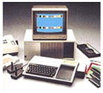
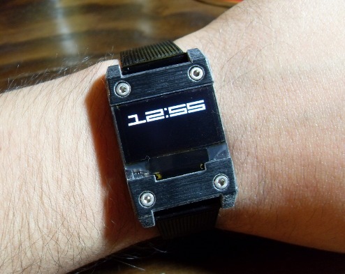
 While TI has introduced many toys for kids, we couldn’t ignore those that are kids at heart. What about something for the rest of us to be filled with awe? In 1975, TI created an awe inspiring LED watch. Introduced at CES in Chicago, the TI LED watch was the first electronic watch using light emitting diodes (LEDs). Retailing for just $20, TI’s model offered new technology at a much lower price, giving consumers access to technology like they have never had before.

It may be hard to think of a watch as awe inspiring, until you lay your eyes on the Pebble smart watch. The Pebble is fully customizable, wirelessly connecting to your smartphone and giving instant access to emails, texts and applications--allowing you to access much of your smartphone’s capabilities from your wrist. TI’s Bluetooth CC2564 dual-mode solution and power and battery management components ensure users will be able to stay wirelessly connected without having to constantly recharge their watch.

The 1980s marked the first time anyone could consider a computer as a toy. Until then, computers graced the campuses of universities and technical companies, but a computer at home was a rare luxury. In 1981, TI introduced the 99/4A, the first 16-bit personal computer designed to out-perform other 8-bit computers in the market. Equipped with a 13-inch video color monitor, it used plastic plug-in modules of read-only memory containing games like Donkey Kong, Frogger and TI Invaders. Other plug-in modules could be used for personal finance and educational programs.

Today, we don’t just buy a computer and use the accompanying software. With the Sitara-processor-based BeagleBone Black and MSP430™ LaunchPad, anyone can design computers for their needs, empowering the imagination of those willing to learn a little bit of code. The maker movement and the rise of an underground do-it-yourself technology culture has gained rapid momentum as these tech toys allow engineers to easily design and program, enabling a new wave of hobbyists to create their own tech toys.  

BeagleBone Black and the MSP430 Launchpad have been used for all sorts of toys from smartphone apps like BeagleStache, to OpenROV, the community of open-source underwater robots used for exploration and education, to the HEXBUG® Aquabot, a robotic fish. All of it made possible by TI technology and the resourcefulness, ingenuity and creativity of people who are passionate about making cool toys.

As we enter the holiday season, it is time to think, and feel, like a kid again. Be amazed at where we have come from (Speak & Spell, Julie Doll, LED Watch, TI 99/4A), and discover where we are going (InfoMotion Basketball, LEGO MINDSTORMS EV3, Pebble smart watch, BeagleBone Black computer, MSP430 LaunchPad). Like us, you can be filled with awe and wonderment about the world around us and the technology that empowers us.

We have so many more TI Toys we want to share with you from the past and the present. Check out this fun infographic of TI Toys through the years:

A Conversation with TI’s ESD Guru

$
0
0

Last week we looked at demystifying ESD testing terminology. This week I had the chance to sit down and talk with Zeb Agha, an ESD Guru at TI with seven years of experience in solving customer’s ESD-related issues. He brought up some common things to look for if you suspect your application is the victim of an ESD-related failure.  

(1) How did the failure manifest? There are multiple ways in which an ESD failure might manifest, for example hard, soft or latent failures. If a hard or non-recoverable fail is observed, a device on the board that is subject to ESD testing is permanently damaged. This can be verified by performing a failure analysis and observing the damage optically or via under a scanning electron microscope (SEM). Boards or devices that are sent back to the manufacturer for failure analysis routinely undergo such testing. Soft failures can manifest as latch-up of specific pins that couple ESD/EMI through conduction or radiation. Latent failures may not show any external symptoms of failure but damage device reliability or reduce the MTBF factor.

(2) What caused the failure? If you have an ESD expert at hand he will most likely be able to look at your board and point out weaknesses and areas of ESD susceptibility with a visual inspection. Is there an unshielded cable that leads from an external interface back to the board? Does the PCB support an independent ground layer? Are there any protection devices next to ESD hot-spots such as a USB connector? If debugging a suspected ESD fail on an MCU and it is a soft failure, we can gain some information by reading the state of the registers when the failure occurred. For example, if the board suddenly seems to stop functioning and a reset of the MCU brings the board back up, reading state registers, program counters etc can provide valuable information on the state of the device at the time of failure. This can be implemented by simple means such as a serial output stream via the UART or using a state trace mechanism via the debugger.

(3) Are there any hot-spots? IEC testing mandates that if the user has an interaction with the PCB such as through a switch, the testing must use contact discharge i.e. the ESD voltage is discharged by touching the external interface directly. In such cases where certain areas in the PCB are known to have increased exposure or higher susceptibility it is important to build in protection via external ESD-protection diodes such as the TPD2E001  a single chip ESD protection array for high-speed data interfaces.

A white paper by Roger Liang, Systems Engineer for the Integrated Protection Devices (IPD) group in TI also highlights a class of protection devices called Transient Voltage Suppressors (TVS). TVSs are placed on general purpose I/Os that are exposed to the possibility of a strike. Under normal operating conditions these devices are open and do not interfere with the GPIO operation. In the event of an ESD strike, the TVS device forms a short circuit path to ground to safely discharge the excess voltage. For more details on how TVSs work and information on system=level ESD design refer to Design considerations for system-level ESD circuit protection.  For a comprehensive list of ESD protection devices, visit the IPD group’s web page or browse through their brochure and select a device that fits your applications needs.

Remember that when an ESD-related failure occurs, it is important to walk through the exact scenario leading up to and after the ESD strike to determine how to prevent or protect the application from future ESD events.

In my next blog post I will discuss some common pitfalls that lead to lowered ESD resistance as well as measures to combat strikes and increase the possibility of passing system-level testing.

Stay tuned.

The buck regulator efficiency/size tradeoff dilemma

$
0
0

As an applications engineer, I know that buck regulator implementations are inevitably tied to a tradeoff of efficiency versus size. While this axiom is true for many switch-mode DC/DC topologies, you can put a long series of exclamation marks after the sentence (!!!) when the application demands low output voltage and high output current, e.g. 1V and 30A. Then, a small form-factor power solution, balancing efficiency and size, is vital.

High efficiency is a key performance benchmark, leading to reduced power loss and component temperature rise, and more useable power at a given airflow and ambient temperature. From this standpoint, a low switching frequency is very enticing, but cost and size increase as large filter components are needed to meet target specifications such as output ripple and transient response.

PCB area dedicated to power management is an immense constraint for the system designer. With that in mind, let’s review the benefits of high switching frequency. First, inductance and capacitance requirements decrease at higher frequency, leading to tighter PCB layout and smaller footprint and profile. A lower inductance allows a faster large-signal change in current, and coupled with higher control loop bandwidth, enables faster load transient response. A rule of thumb for maximum loop bandwidth is 20% of switching frequency. Last, some interesting options open up at higher frequencies in terms of component selection.

For example, take a look at this regulator design that exploits careful component selection to push efficiency/size/cost boundaries.  Watch a video demonstrationhere.

Schematic of 600-kHz step-down regulator rated at 30A

(1)  Inductor - Even though iron powder or composite core inductors give commendable performance at low frequency, higher core losses negate their value proposition above 500kHz or so. At that point, ultra-low DCR ferrite magnetics tend to offer lower copper and core losses. Note that core losses are easy to gauge, at least on a relative basis, by looking at a converter’s no-load input current. Off-the-shelf options for ferrite inductors with single-turn “staple” winding are widely available, and sub 1-mΩ DCR is easily achieved if only one winding turn is required!

(2)  PWM Controller - Now, if a design is captive to the hard saturation characteristic of a ferrite-cored inductor, it’s imperative to never exceed the inductor’s saturation current. This points to a PWM controller that leverages parasitic circuit resistance(s) for accurate yet lossless current sensing (read my previous blog, “Nailing Accurate and Lossless Current Sensing in High-Current Converters" for more on this topic). Other salient features include efficient gate drivers, remote BJT temperature sensing, and fast error amplifier.

(3)  MOSFETs - Power semiconductors are the cornerstone to gaining advances in efficiency and size. Consider, for example, the Power Block NexFET™ family, oft-praised for innovatively co-packaging high- and low-side MOSFETs by vertical stacking. When frequency-proportional losses warrant a close eye, low QG, QRR, QOSS charges are vital. Low RDS(ON), high current copper clips, kelvin gate connections, and grounded tab are essential, too.

(4)  Capacitors - At higher frequencies ceramic capacitors are favored over electrolytics. Now, output bulk energy storage becomes redundant as the control loop promptly reacts to transient demands. Ceramics offer not only lower ESR but also lower ESL, which mitigates output ripple from inductive divide effect and low filter inductance.

What other factors affect regulator efficiency and size? Popular themes of late include GaN MOSFETs, and power-system-in-package (PSIP) and -on-chip (PSOC).  Let me know what you think?

Resources: 


DSPs – they’re on every toy’s wish list this year

$
0
0

It is pretty well known that DSP began life as a voice processor for the iconic Speak and Spell toy. Speak and Spell may have achieved icon status on its own, but when ET hacked it to phone home its place in the toy hall of fame (if there is such a thing) was secured. DSP of course went on to greater heights as the workhorse of the mobile communications revolution powering both the modems in our mobile phones and the base stations that form the mobile infrastructure. Arguably the smart phone is in part a sophisticated toy, so the DSP’s role as an engine of play continues.

DSPs are still used in standard children’s toys today. And many next generation toys are focusing on voice as the primary user interface because it is the most natural interface, especially for young children. These toys will be interactive, as in, the child talks to the toy and it responds. The speech detection, analysis and speech synthesis functions required to support this are very processor intensive so the power/performance profile of DSPs makes them a great choice for this application.  

I haven’t seen any cloud enabled toys yet, but you know that has to be coming. DSP enables a great natural language interface, with always-on ease of use and great battery performance. Adding connectivity can make the experience boundless and evolving. If you add wireless charging to the mix, a child could put their toy to bed at night and it will wake ready and refreshed in the morning. No cables, no plugging in, no on/off switches. What a great formula for bringing a toy to life!

 At the other end of the spectrum are toys for big kids. Today, DSPs are critical to the advent of safer cars where they are increasingly providing the data and video analysis that is behind Advanced Driver Assistance Systems (ADAS). They are also critical in enhancing the driving experience through advanced in-car infotainment systems. Let’s face it; once we get beyond basic transportation, cars are the ultimate toys for many of us. Another big kid toy is this DSP powered basketball which clearly falls into the “what will they think of next” category. I’m hoping that people who have members of the Washington Wizards on their holiday gift list will read this and take the hint. They could use it!

So given the exceptional power and performance of DSPs, what are you thinking of for your next toy design?

Future battery chemistries: lithium / sulfur

$
0
0

While Lithium-oxygen is the ultimate prize for high energy density-seeking battery companies, it has severe issues with power capability -- especially since you need to force the fleeting gas (oxygen from air) to react fast enough to keep up with state-of-the-art solid state batteries. This issue made everybody look at sulfur, which does not have the concentration problem, being a solid and otherwise similar to oxygen in reactivity. Sulfur enables slightly less energy density because it is a less aggressive non metal (so voltage would be 2.4V instead of 3V), and it is lightly heavier because of its position on the third row of the periodic table. However, a Li / sulfur battery theoretically offers 2550 Wh/kg, which is more than five times higher than the best available Li-ion battery. This is a prize worth pursuing. And for the past 30 years many companies have attempted to create batteries with high densities. But like with all promising technologies, there are lots of hurdles – if there was none, it would have been done years ago. The trick is to attempt to commercialize a new chemistry at the right time – when material science has offered just the right new tools to solve the old problems, and at the same time the demand is so high that it can justify higher price for higher performance.

Is now such time for Li / sulfur? It remains to be seen, but let's look at the actual problems and new solutions. And maybe we can make an educated guess on chances of overcoming them.

Low conductivity. To provide electron flow active material needs to be electrically conductive. Sulfur is an insulator, so it need to be mixed with some conductive additive to bring electron flow very close to its surface where reaction will take place. The more additive the better the conductivity, and also the higher the contact area with sulfur, which speeds up charge transfer reaction so power capability increases. Unfortunately this conductive matrix occupies some volume and has some weight, which cuts into the energy density. In fact, the best commercial Li/S batteries (Sion Power) that have decent power capability are at 350Wh/kg, which is more than seven times less the theoretical level and does not even beat traditional LiCoO2 based cells. New tools to solve the problem? Nanotechnology. By making the matrix out of material specially shaped on nano-scale, they can retain high conductivity and high surface area needed for wide contact with sulfur while having itself low profile and weight. The kind of nano-structures considered vary widely. Carbon nano-wires are popular because they have great conductivity along their length, while keeping weight to the minimum. Carbon foams and graphene “petals” that resemble flowers are popular to increase surface area. Sulfur itself is being prepared as nano-sized particles or films deposited on carbon structures.

Sulfur solubility in the solvent. In a battery it is desirable that cathode material would stay where it is -- attached to positive current collector. If it can freely wander through the cell, it can contact the anode material directly and wastes the energy by reacting with it instead of passing the electrons over the external circuit. Unfortunately that is exactly what happens with sulfur cathode because sulfur atoms tend to make chains, circles, etc. with each other, which causes it to react with dissolved reduced product Li2S by forming polysulfide with general formula L2(Sn) where n can be very large number. This way sulfur is carried to various places in the cell and can be deposited far away from the carefully designed carbon structures that are supposed to contact it. This way sulfur is lost, and energy can not longer be extracted from the cell. For this reason even the best Li/S batteries typically show only 300 cycles vs 500-1000 cycles of rational Li-ion. To add insult to injury, sulfur can even be deposited very close to Li-anode reacting with it directly and creating potentially unsafe mix. What can be done with it? Again nano-structures to the rescue. A popular solution proposed by Prof. Yi Cui group is to put active material, such as sulfur or silicon as a “yolk” in the middle of oversized “eggshell” of conductive protective layer. When “yolk” is charged it is growing just like the chick embrion in an egg, but still has enough space without cracking the shell. The shell prevents polysulfides from leaking into the solution while also providing close electric contact. A similar solution is to pack sulfur inside carbon nano-tubs so that when it expands in stays inside like meat inside a sausage.

Fig.1 A Yolk-Shell Design for Stabilized and Scalable Li-Ion Battery Alloy Anodes, Nian Liu, Hui Wu, Matthew T. McDowell, Yan Yao, Chongmin Wang, and Yi Cui

Lithium safety. With everybody concerned about the safety of present day Li-ion cells, we are forgetting that Li-intercalation graphite anode itself was invented as a safe replacement for highly unstable Li-metal anode. After Moly Energy Li-metal battery factory fire in the nineties, no serious mass manufacturer was considering making a Li-metal rechargeable battery. Li-dendrites growth during charge is too unpredictable and can short the electrodes with catastrophic results. Luckily, polysulfides have an unexpected side effect of shaving off the growing Li-dendrites by reacting with them, and passivating the Li surface with solid electron-insulating Li2S layer that is mechanically strong and even stopping short-circuits under mechanical cutting or piercing the battery. Unfortunately the same layer makes their internal resistance quite high, cutting down battery power capability. Better solution would be to replace Li-anode completely with something more safe yet higher energy than tradition graphite, like Si-anode. But in this case we would need to have some source of lithium in the system. One way is to assemble cathode in discharged state as Li2S but it is difficult to deposit it in nano-shape since it is highly unstable in presence of water. Another approach is to still use much cheaper elemental sulfur, but add lithium in form of passivated lithium powder (such as provided by FMC corporation) to either anode or cathode and let it react on the spot once electrolyte is filled. This is an innovative approach that might help with many new interesting materials that could provide large energy but don’t come as convenient Li-containing compound.

Solvent flammability. Like all other high-energy batteries, Li/sulfur would have to use organic solvent, since water is violently reacting with lithium. Unfortunately all organic solvents are flammable, which is already a concern with present day Li-ion batteries but will be even more a concern when Li-metal is used. Interesting approach is to get rid of solvent completely and just use a very thin layer of solid electrolyte between anode and cathode. Solid electrolyte is a ceramic and cannot burn at all! More and more solid state materials that can conduct Li is being discovered, and this is an exciting area of research for any kind of Li-ion battery but particularly for Li-sulfur since products of its burning are SO2 that is much more irritating than for traditional Li-ion batteries case.

Based on all above advances, when will we see Li-sulfur batteries on store shelves?

Several companies in particular Sion and OXIS are offering prototypes for testing already. First applications are likely in next few years outside of consumer space, such as grid storage, where high energy density and low cost are key, while concerns of burning sulfur in the middle of the Arizona desert are reduced. As safety is proven and device makers familiarity with this chemistry increases, I expect to eventually see them in portable devices, since five times higher energy density is just irresistible to modern ultra-compact energy hungry gadgets.


Additional Resources:

Viewing all 4543 articles
Browse latest View live


<script src="https://jsc.adskeeper.com/r/s/rssing.com.1596347.js" async> </script>