Quantcast
Channel: TI E2E support forums
Viewing all 4543 articles
Browse latest View live

How to improve the startup and stop behavior of ERM and LRA actuators

$
0
0

Eccentric rotating mass motors (ERM) and linear resonant actuators (LRA) are commonly used in smartphone and tablet applications to provide tactile feedback through haptic effects.   While there are many characteristics to consider when designing for haptic feel, one of the most noticeable traits to users is the start and stop time of the actuator. 

The start time of an actuator is the time it takes to go from 0% (or driver off) to 90% of the maximum acceleration.  Likewise, the stop time is the time it takes for the actuator to go from when the driver waveform ends (or driver turns off) to 10% of the maximum.


       Figure 1:  Start Time                                                    Figure 2:  Stop Time

This start and stop time translates to a qualitative feel that a user will identify as “sharpness” or “crispness.”

The start time is analogous to a car’s “0-60” time.  Let’s take two cars, one is a fast sports car and the other is an inexpensive compact.  Both cars are stopped at a red light.  When the light turns green, both cars slam the accelerator to the floor and begin moving.  The sports car has a sharp burst of speed and quickly leaves the compact in the dust.  Meanwhile, the compact is only halfway across the starting line and is far from reaching full speed.  


Figure 3:  Overdrive and braking is analogous to 0-60 speed times.

Likewise, some actuators will have very quick start times and others will have very slow start times.  It depends on the design, manufacturing and type of actuator, all of which can be characterized empirically in the lab.

For haptics in touch screen smartphones, users may notice a keyboard click is sharper in one phone compared to another.  This is due to the response time of the actuator.

To improve the actuator performance, the actuator driver can overdrive it to obtain a quicker start time and reverse drive for a quicker stop time.  For ERMs, overdriving is achieved by applying a higher DC voltage at the beginning, and applying a negative voltage to brake.


Figure 4:  ERM Overdrive and Braking Drive Waveform

For LRAs, overdriving is achieved by applying a higher AC voltage at the beginning, and applying a 180 degree out-of-phase signal to brake.


Figure 5:  LRA Overdrive and Braking Drive Waveform

TI’s new DRV2605 haptic driver has a feature called “smart loop,” which uses closed loop feedback to apply the exact overdrive and brake signal to maximize the start and stop time of an actuator.  Smart loop does this by actively monitoring the electromotive force (back-EMF) signal of the actuator to accurately control the drive voltage and acceleration. 

The result is automatic overdriving and braking for ERMs and LRAs that simplifies software programming and reduces startup and braking time by 50 percent. And the DRV2605’s automatic actuator diagnostics and level tracking feature delivers consistent acceleration over a wide range of environmental conditions. If you want to get from 0-60 faster than the competition, take the DRV2605 out for a test drive. You’ll win, every time!


Electric Avenue: TI’s Texas sites experiment with electric vehicle charging stations

$
0
0

It’s a subject that’s been hot in the news: the number of Electric Vehicle (EV) charging stations is on the rise. Now, a new federal-funded project is making it easier for TIers to power up their electric vehicles. In April, TI’s Worldwide Facilities department is installing 46 Blink network Electric Vehicle (EV) charging stations at 12 different TI sites across Texas.

 Through a government and private-industry partnership designed to accelerate EV adoption, TI is installing the charging stations at no cost, and will evaluate them throughout the year. At the end of the evaluation period, TI can choose whether to leave the stations in place or remove them. (Want to see a map of Blink’s 289 Dallas stations? Click here.)

Other charging station locations will include TI’s Sherman manufacturing facility, which will receive four, and TI’s Richardson manufacturing facility which will receive two. The locations were selected based on building population and access to nearby power sources.

Steve Moore, a 31-year TIer and self-described “car nut,” is manager of central utilities and is helping to roll out the project. “I hope that the program becomes very popular and our employees look at it as another benefit,” he says. “TI has multiple products that go into electric cars, so in a way, we’re helping support our own technology.”

TIer Guy Josselyn, a strategy team manager for TI’s design systems IT group, agrees. Josselyn drives a 2012 Tesla S Model, and has been giving Moore’s team feedback for the past year.

“I’m a very big supporter of TI doing what it can to alleviate our footprint from an environmental standpoint,” Josselyn says. “Anything we can do to move toward having flexibility is a good thing for our country and opens up new technologies and ways to save energy, transfer energy and store energy.”

The Level 2 fast-charging stations will be operated by electronic transportation company ECOtality on the Blink network. Because it can take up to eight hours to charge an electric vehicle (depending on amount of discharge), Blink sends emails or texts to alert car owners when their charge is complete.  The stations at the TI campuses are designed to supplement home chargers, and charge $1 per hour, the standard rate.

These new EV stations are the first official stations at TI – but not the very first. About a decade ago, a former TIer built his own electric vehicle, and TI facilitated an onsite spot where he could park and re-power. “We were cool before it was cool to be cool – old-school cool,” Moore says with a laugh.

We’re, ahem, energized, either way.

TI's spotlight session at ECEDHA “TI, an education partner like no other”

$
0
0

Larissa Swanland, TI’s Worldwide University Marketing Microcontroller Manager presented a spotlight session in the 2013 ECEDHA Annual Conference and ECExpo last week. She presented “TI, an education partner like no other” to the largest gathering of ECE (Electrical and Computer Engineering) department heads throughout North America. Sad you missed it? Let me summarize!

Larissa began with an overview of Texas Instruments – a global semiconductor design and manufacturing company, operating in more than 35 countries, serving more than 100,000 customers worldwide, innovating for more than 80 years, with more than 100,000 analog ICs, embedded processors and software and tools, and a total revenue of $12.8 billion. Then began a deep dive into TI’s University Program- we offer educators discounted tools, free products, and lab donations so students can learn TI technology in teaching labs that are smarter and more fun. From teaching materials to design projects, our advanced Analog and Embedded Processing technologies fuel the passions of students and educators in more than 4,000 universities worldwide.

Larissa then went in depth around TI’s embedded processing tools, products and resources. TI microcontrollers offer the broadest range of options. We offer the spectrum of low power, low cost, entry level processors to the higher power, highly specialized application specific processor. These include TI’s MSP430 ultra low-power, 16-bit microcontrollers, C2000 real time control microcontrollers with DSP function, Stellaris general purpose ARM® Cortex-M4F 32-bit microcontrollers, and Hercules ARM Cortex-R4 32-bit microcontrollers. Larissa further highlighted TI’s LaunchPad: a low-cost, fully featured development ecosystem that is designed to have the lowest barrier of entry to TI’s microcontroller portfolio. Available on the MSP430, the C2000 and Stellaris, the LaunchPad is a cohesive Ecosystem consisting of hardware, software, community of support and additional add-on boards. At a sub-$20 price tag, it’s no wonder it’s proliferated over 300 university curriculums and sold over 400,000.


Design your own hardware to expand your LaunchPad/make your own BoosterPack and share your projects and your experiences with the rest of the LaunchPad community. Build your own BoosterPack for the LaunchPad ecosystem and turn your BoosterPack into a product! BoosterPack modules plug in to the header pins on the LaunchPad and allow to you to explore different applications that your favorite TI MCU can enable. There is a broad range of application-specific BoosterPacks available from both Texas Instruments and third parties, including capacitive touch, wireless sensing, LED lighting control and much, much more. BoosterPacks are available in 20- and 40-pin variants and multiple BoosterPacks can plug into a single LaunchPad to greatly enhance the functionality of your design.

TI University Program also offers FREE software development environment with the hardware. We encourage as many options to be available without any preference, but also provide a free software to academic instructors and students. Code Composer Studio™ (CCStudio or also known as "CCS") is an integrated development environment (IDE) for TI's embedded processor families. CCStudio comprises a suite of tools used to develop and debug embedded applications. By using CCStudio, instructors and professors can have 'One Install for All' making maintenance of shared lab equipment easy and support of all TI microcontrollers, microprocessors or DSP's possible on student owned copies.  

Our broad embedded processing portfolio and accompanying software allow students to gain familiarity with TI at the earliest point of their Engineering Curriculum, but it also scales to more advanced Integrated Development Environments and complimentary tool chains during more advanced curriculum.  TI covers everything from Intro to Engineering all the way to Senior Design.

To supplement TI’s tools, hardware, and software offering – TI bundles them all with educator developed teaching materials. These teaching materials are designed to help make the development of course materials seamless. TI’s Teaching ROMs are written by educators for educators and include introductory overviews to TI’s MCU or DSP, a walkthrough of the various architectures, and updated labs for today's most popular platforms. They are available to download or you can request a copy on CD free of charge. TI also offers a large selection of TI recommended engineering textbooks supporting analog, MCU or DSP curriculums. Educators can now collaborate across curriculums, schools, and countries within TI’s teaching repository. Share your course material or explore your fellow educators posted materials. Leverage this online resource to get informed and stay ahead.

 In summary, TI encourages professors to enrich their students education with more hands-on project based learning. The TI University Program makes it easy to teach students on the latest industry products from TI.

  • Hardware: Fully Featured With everything you need ready to go at prices that are manageable
  • Software Development Environment: Development Environment that matches the skill set of the user either by TI or software partner
  • Teaching Materials: Creation of a community and shared bodies of knowledge
  • Services value added: Enabling a network of providers to go beyond T,I IEEE, Third Party Partners

How to decide which MSP430 MCU is right for your application with an LCD

$
0
0

Welcome to the MSP430 LCD Blog Series!  Our team will take you on a three-part ride to learn what MSP430 MCUs have to offer for displaying all that cool data you guys are generating.  We get a lot of questions about our LCD portfolio because there are so many tempting features to choose and developers don't always know what's the best option for their design.  Here’s what you can expect to learn in the next few weeks:

  • Part 1:  TI's MSP430 LCD portfolio and how to decide which MCU is right for you
  • Part 2:  Applications and benefits of using an integrated LCD
  • Part 3:  Selecting a development tool for LCD applications

The ride is ready to begin.  Here we go...

Back in 2001, MSP430 released its first microcontroller with integrated LCD.  Since then, we've developed a strong portfolio that has grown to support more than 100+ devices with LCD and integrated memory of up to 512kB Flash.  This provides you, our customer, with the industry’s broadest offering of microcontrollers with integrated LCD and high memory options to support endless low power applications (Seriously, what ISN'T using a display nowadays?)

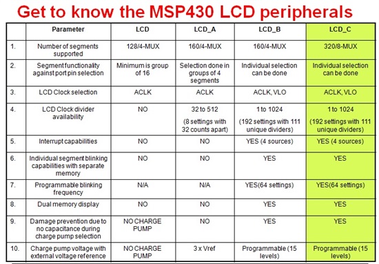
As the MSP430 microcontroller has grown, so has each peripheral - including our beloved LCD.  Features such as the number of segments, clock dividers and programmability of segments have expanded with the latest microcontrollers.  It’s now easier than ever to individually control the blinking of each segment, dual displays and interrupts with the 320-segment LCD_C.  If you're having trouble deciding which features are important to control the display in your application, the table below provides many details on the features and differences between the LCD peripherals across our portfolio.


Now that you're decided which features are most important for your application, take a look at our various ultra low power MSP430 series with integrated LCD.

4 series– up to 16MHz and 120kB Flash; featuring 16-bit Sigma Delta, 12-bit DAC, Operational Amplifier

6 series– up to 25MHz and 512kB Flash; featuring 24-bit Sigma Delta, RTC with battery backup, USB, 12-bit DAC, Operational Amplifier

RF SoC series– up to 20MHz and 32kB Flash; featuring sub-1GHz RF Transceiver, 128-bit AES for security


The MSP430 LCD portfolio is the best option for any developer using an LCD.  Stay tuned for our next segment on this blog, where we'll evaluate different applications and the benefits of using an integrated LCD in your next design.

To Be Single or Differential, That is the Question

$
0
0

Single Ended or Differential?Whether 'tis nobler to signal via complementary means, or to take arms against a sea of noise… ah, but I take literary license with Shakespeare.  But it does raise a real question… should a designer use differential or single ended methods for carrying analog signals?  The answer also contains a question… which is, “it depends on the SNR requirements” or “it depends, what are the system requirements?” to be exact. In high performance systems, noise can be everywhere, but will that warrant the additional complexity of differential signals?

In low speed signaling it is much simpler to use a single (ground referenced) signal.  In the singled ended mode there are two options – unipolar and bipolar.  The unipolar option swings the signal between V+ and ground.  This is common for single supply systems and can actually be configured in a bipolar fashion with biasing (more on this in a minute).  Bipolar signaling in classic sense swings the signal between V- and V+ centered at ground.  Many operational amplifier circuits are designed with this type of signaling and (NOTE: IMPORANT INFORMATION FOLLOWS) will not work with a single supply op-amp (e.g. +5 and ground).  However, by moving the bias point of the amplifier to V+/2, you can emulate the split supply bipolar system and the standard op-amp circuits will again work (more in an upcoming blog post). In this configuration, the bias voltage (+2.5V in the example) is the new virtual ground reference.  All signal references are made to this voltage.  If you AC couple the input signal it will be bipolar relative to the Vbias voltage (the virtual ground).  In our example “working” inverting amplifier that would look like +/- 2.5V signal input relative to +2.5V bias – output would be inverted relative to the same bias voltage.

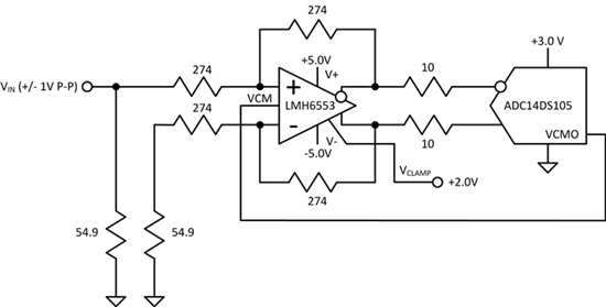
As signal speeds increase, the voltage swings are reduced to mitigate capacitive loading.  It is not uncommon to see 1 - 2V or +/- 1V levels driving (capacitive) cabling.  As frequency content increases, it is often a requirement to move to differential pairs (and controlled impedance transmission lines) which are terminated at both ends.  The termination is both to generate a voltage for the receiver or amplifier and to terminate the transmission line to limit reflections.  But what if an engineer has a design using a high speed input signal and needs to convert it to a differential signal.   This is common for designs using high-speed analog to digital converters such as the ADC14DS105.  This ADC has differential inputs… so they can either transformer couple which will degraded low frequency response or use the circuit shown below.  This circuit DC couples the bipolar signal resulting in DC accuracy – important for applications such as video… it also uses a unique differential amplifier - the LMH6553 - which has a protection clamp on the output.  This prevents large input swings from damaging the ADC - something that could happen if the input is a connector on the outside of the equipment!  In addition, the circuit below is terminated for 50 ohm transmission lines.

Bipolar to Differential ADC Front End

Schematic of single ended to differential ADC front end

Hope this brief discussion enlightens you to the trials and tribulations of single versus differential signaling. I’ll elaborate on this topic and some more op-amp circuits (if you like them) in future posts… till next time!

Teaching Your PI Controller to Behave (Part VI)

$
0
0

Dave Wilson, Motion Products Evangelist, Texas Instruments

I am writing this particular blog installment while lying by a swimming pool in a resort on the Riviera Maya.  There are lots of beautiful distractions which are competing for my attention, including my gorgeous 20 month old granddaughter who is playing at my feet.  So I have to disclaim any liability related to the quality of this particular blog!

So far in this series we have discussed how to set the coefficients for the PI controllers in a cascaded speed control loop.  We saw that Kb is used for pole-zero cancellation within the current loop.  Kc and Kd are indexed to the velocity feedback filter’s time constant, and are calculated by first selecting a suitable damping factor which is related to the responsiveness and damping of the system.  We also saw that Ka sets the current controller’s bandwidth.  But what should that bandwidth be? 

It turns out that we have two competing effects vying for control of where we set Ka.  On the bottom end of the frequency range, we have the velocity feedback filter pole with some really nice tan lines that wants to push the current controller pole to higher frequencies so as to not interfere with our nice tuning procedure.  But we can only go so high before we start running into other problems.  Let’s take a look at both ends of the frequency spectrum in an effort to understand these issues, and hopefully gain some insight into how to judiciously set Ka.  But first, let’s rewrite the open-loop transfer function of the velocity loop to once again include the current controller’s transfer function:

                          Equ. 1

where:      K is a coefficient that contains several terms related to the motor and load

                Kc and Kd are the PI coefficients for the velocity loop

                L is the motor inductance

                Ka is one of the PI coefficients for the current loop

                t is the time constant of the velocity feedback filter

                s is the Laplace frequency variable

Our tuning procedure assumes that the current controller’s closed-loop gain is always unity, which implies it has infinite bandwidth.  But in reality, as long as the current controller’s bandwidth is at least 10x higher than the velocity loop unity gain frequency, our tuning procedure is still pretty good at predicting the system response.  If this condition isn’t satisfied, the current controller pole starts interfering with the velocity loop phase margin, resulting in a more underdamped response than our tuning procedure would otherwise indicate.

Figure 1 shows an example case to illustrate this point.  The green curve represents what the tuning procedure predicts the normalized step response should be for a system with a damping factor of 2.5.  The red curve shows what happens when the current controller’s bandwidth is reduced to equal the velocity filter’s bandwidth.  The system is still stable, but the damping is much less than predicted from our tuning procedure.  At this point, we have two options…either increase the damping factor (and consequently lower the frequency response of the velocity loop), or increase the current loop bandwidth by increasing Ka.  The cyan curve shows the first option where we increase the damping factor just enough to bring the overshoot down to the predicted value.  Unfortunately this increases the step response transient time as well.  The yellow curve shows the latter option where we put the damping factor back to 2.5, and increase the current controller’s pole to be 10x higher than the velocity loop unity gain frequency.  As you can see, the actual response more closely resembles the predicted value.  The higher the current controller’s bandwidth is, the closer the response will resemble the predicted response.

Figure 1.  Step Response of a System with Variable Damping and Pole Placement

So from this exercise, we might conclude that the best strategy is to set the current controller bandwidth to be as high as possible.  But is this really the best course of action?  As my dear ol’ grandma used to say, “Never use a 1 GHz op-amp when a 1 MHz op-amp will do the job.”  (Well, she never actually said it in those exact words, but you get the point).  Usually high bandwidth in any system results in unruly and obnoxious behavior, and should only be used if absolutely necessary.  In this case, high current loop bandwidth often results in undue stress on your motor, since high frequency current transients and noise translate into high frequency torque transients and noise.  This can even manifest itself as audible noise!  But there is also another limit on your current loop bandwidth:  the samplingfrequency.

Take a look at Figure 2 which shows a digital Field Oriented Control (FOC) based Variable Frequency Drive (VFD).  To simplify the discussion, we will assume that the entire control loop is clocked by a common sampling signal, although in real-world applications we often choose to sample the velocity loop at a much lower frequency than the current loop to save processor bandwidth.

Figure 2.  Digital Field Oriented Control System for a PMSM.

In an analog system, any change in the motor feedback signals immediately starts having an effect on the output control voltages.  But with the digital control system of Figure 2, the motor signals are sampled via the ADC at the beginning of the PWM cycle, the control calculations are performed, and the resulting control voltages are deposited into double-buffered PWM registers.  These values sit unused in the PWM registers until they are clocked to the PWM output at the start of the next PWM cycle.  From a system modeling perspective, this looks like a sample-and-hold function with a sampling frequency equal to the PWM update rate frequency.  The fixed time delay from the sample-and-hold shows up as a lagging phase angle which gets progressively worse at higher frequencies.  Figure 3 shows a normalized frequency plot of the phase delay for a sample-and-hold function, where the sampling frequency is assumed to be 1.  As you can see, the phase delay reaches down into frequencies much lower than the sampling frequency.  For example, at one decade below the sampling frequency, the S&H is still affecting a phase shift of -18 degrees.

Figure 3.  Phase Lag Plot for a Sample-and-Hold, Fs = 1

 Since the current controller processes higher bandwidth signals than the velocity loop, it is usually the current loop that suffers most by the S&H effect of the PWM module.  Since the PWM S&H is in series with the signal path for the current loop, its magnitude and phase contributions add directly to the open-loop response for the current controller.  If we rewrite the equation for the open-loop response of the current controller (assuming Kb = R/L), we end up with the following function:

               Equ. 2

This is simply an integrator function with gain of Ka/L.  Unity gain will obviously occur when s = Ka/L.  The single pole at s = 0 implies that the unity gain frequency will have a 90 degree phase shift, which also implies a 90 degree phase margin.  However, for a digital control system, you must add the phase lag shown in Figure 3.  To do this, calculate for the following frequency ratio:

                  Equ. 3

Then use Figure 3 to determine how much phase lag you must subtract off of your phase margin.  For example, if KaTs/(2p L) = 0.1, then you must subtract off 18 degrees from your phase margin, leaving you with a comfortable 72 degrees.  In most designs you probably want to keep Ka/(2p L) at least an order of magnitude below the sampling frequency.  So using this assumption as well as the constraints from the velocity loop tuning procedure, we can now write a general “rule of thumb” expression for the range of Ka:

                                                           Equ. 4

where:     L is the motor inductance

                t is the velocity filter pole

                d is the damping factor

                Ts is the sampling period

In most designs this still leaves a fairly broad range for the value of Ka.  In my experience, I have found that erring on the side of the current bandwidth being too low is usually better than being too high.  Snappy waveforms look nice on an oscilloscope, but your application may not need (or want) all that bandwidth. 

Up until now, we have only dealt with “small signal” conditions (i.e., linear operation with no saturation effects).  But in the real world, step transient responses almost always saturate the system’s voltage or current levels, which tend to lengthen the response times.  When this happens, you can increase the PI gains all you want, but it won’t speed up the response.  In fact, it will usually just make the overshoot worse, since the integrator is acting on a gained-up error signal, which it will just have to dump eventually.  So how do we deal with this problem?  Are we doomed to simply using low integrator gains?  It turns out that there is another solution which doesn’t involve changing your integrator gains, which I will discuss in my next blog.  Until then…

 Keep Those Motors Spinning,

Op Amps… G=1 stable & decompensated

$
0
0

You have voted. Unity-gain-stable op amps won in a landslide—they’re far more popular than decompensated op amps. What’s this all about?

Click Here to read on EDN Magazine site.

Develop a Bluetooth Smart sensor app in one hour

$
0
0

In cooperation with Bluetooth SIG we will present a webinar how to develop Bluetooth Smart (low energy) apps based on the SensorTag. Join us to learn how to get started with app development for Bluetooth accessories!

Register now

Date: Wednesday, April 17, 2013 
Time: 8:00 a.m. (PDT) / 11:00 a.m. (EDT) 
Duration: One hour

Archived webinars will be available here

Jarle


Testing power supply: Measuring efficiency

$
0
0

During my normal activity as an Analog Field Applications Engineer, I am called to help a customer solve system problems. These system problems sometimes relate back to the power supply.  Last year, over a period of 3 months, I had 3 different situations at different customers where the root cause of a system problem was a relatively straight forward power supply design problem. Systems were in production, but problems were arising based on intermittent field failures.  In each case, I discovered that the power supply needed a minor design change which could have easily been identified and implemented before the system was released to production.

What I found most interesting was that because of our advancement in software design tools, customers are placing much more trust in power supply designs without performing what used to be fairly standard bench testing.  In cases, I observed system designers used the results from simulations tools as a strong indication of the robustness of a design, thus not placing as much time (if any at all) on actual bench testing of the power supply.  This observation, with the fact that many designers have never gained experience with bench testing, left me with the clear realization that an article was needed on the subject.  I sometimes wonder how much of this relates back to the current de-emphasis on hands-on design and test in universities, where software tools are replacing these tasks… but that is a topic for a future blog.

That being said, why is testing power supply so important?

As explained above, if a power supply is not fully tested it may leave a system in a marginal state of operation.  A marginal design can result in system failures once the system is deployed and operating in different environments.  System components vary slightly over time which can result in failures of a system that was not fully tested and/or analyzed.

Here is a simple procedure for accurately measuring efficiency:

  1. Before connecting the DC power supply to your power circuit, set the proper input voltage and verify correct polarity.
  2. Connect a voltmeter to the input and output of the power supply close to the input and output connectors.
  3. Connect a current meter to the input and output, see earlier comments.
  4. Connect the electronic load to the output and set it to the lowest value of interest.
  5. Turn on the input voltage and set it to provide exactly the nominal input voltage across the power supply input. Important: Input voltage accuracy may need to be within a few millivolts to ensure overall accuracy and needs to be adjusted after each time the load is changed.
  6. Record the input and output current along with the output voltage. The input voltage is fixed by step 5.
  7. Increase the load at regular intervals up to a load at or above 100 percent. Testing up to 110 percent of maximum load or greater is valuable to help understand operating margins.
  8. Plot curves of the output power over the input power (*100) to show the peak efficiency and efficiency at different loads (Figure 3)

Find more detail on how to measure efficiency of a power supply in my full article on EDN.

You can walk through the process with me in this Engineer It video on how to measure efficiency of a power supply:


Part 2 on measuring noise, and part 3 on measuring stability coming soon.

Why do you think fewer designers are testing their power supply?

Take Ten: Q&A with TI characterization manager of precision analog Scott Gulas

TI “On the Grid” at DESIGN West 2013

$
0
0

Heading to DESIGN West in San Jose later this month? Make sure you stop by TI’s booth (#1607) to explore TI’s latest products from across its embedded portfolios. You will also see our smart grid products in action for metering, grid infrastructure and smart homes/buildings appliations.

Here are the highlights:

Metering:

  • TI’s Energy Watchdog tool can be used to accurately measure power consumption of any household electrical appliance. The power measurement is performed using the MSP430AFE253 energy metering IC and results are displayed on a LCD screen.

Grid Infrastructure:

  • TI’s new Smart Data Concentrator Evaluation Module EVM pushes the smart grid to the next level. Based on TI’s Sitara™ AM335x ARM® Cortex™-A8 processors, the EVM includes advanced hardware and software that reduce development time by up to nine months while still supporting connectivity to more than 1,000 smart meters. The Smart Data Concentrator EVM expands the functionality of designs and enables quick connectivity to the smart grid.

Smart Homes and Buildings:

  • TI is showcasing how easy home automation can be with wireless connectivity solutions. ZigBee and Wi-Fi connected LED lighting, appliances, entertainment equipment and more so consumers have more control and monitoring capabilities inside or outside the home.
  • TI’s ZigBee solutions allow local control via remote that communicates directly to LED bulbs or remotely through a gateway, which is based on an AM335x BeagleBone Linux computer. The kit revolutionizes ZigBee-enabled LED lighting making it easier to develop new networked lighting products for home and building automation.
  • The SimpleLink™ Wi-Fi CC3000 model home demonstrates how simple home automation can be. TI’s CC3000 module combined with the MSP430FR5739 microcontroller help users monitor and control home applications through a smartphone or tablet including a thermostat, window-breaking sensor, fan with light, and an RGB light.

We hope to see you at DESIGN West April 23-25!

Get that cow out of my shower!!

$
0
0

Photo credit: Sylvia Wright / UC Davis.

There are more than 6 billion people on planet Earth and with cows fast approaching the 2 billion mark, there is a high probably, as silly and preposterous as it may seem, that a cow has ended up in someone’s shower. I came from the cow-rich state of Wisconsin, but it does not mean I experienced it – but someone out there is either too ashamed to admit or has missed a golden opportunity to grab their 15 minutes of fame (and missed the next big thing since the Kardashian’s ). Anyway, you may ask how we can avoid this incident (or stop it from happening again– depending on your point of view). 

You’re probably wondering what cows, showers and ultra-low power microcontrollers have in common: Well, the recent release of MSP430G2xx4/G2xx5Value line microcontrollers with more memory can be used in various applications that will definitely prevent this awkward situation from happening again (and stop any incriminating photos from leaking out).

Speaking of cows, have you ever wondered where these natural and energy-efficient lawn mowers come from in the first place? If you are looking for the end-product like a burger, then I suggest stopping by any local fast food joint. But if you’re looking for live ones, check out your nearest dairy farm or any street corner in Wisconsin.

Seriously speaking, modern dairy farms have deployed passive RFID tagging systems to identify cows within a specified range. This system works well if there is only one cow that needs to be identified at a time. It does not work so well if you have multiple cows within a close area. Typically, the cow tag with the strongest signal wins. This is why you see cattle ranchers guide their cows in single file, like elementary school children, as they enter a holding pen to ensure that there is no way to miss a cow’s signal. This isn’t the most practical way to run a dairy farm.

Employing an active wireless tagging system that incorporates an ultra-low power (ULP) microcontroller provides more intelligence while paired with the proper wireless radio/s. The MSP430G2xx4/G2xx5Value Line microcontroller series is perfect for this application because it can now support up to 56K Flash and 4K SRAM, available in a tiny 3.3 x 3.3. mm DSBGA package, and is ultra-low power. The larger memory on these low-cost MSP430 MCUs helps support  the necessary wireless protocol stack, the small DSBGA package size minimizes the solution footprint, while the ultra-low power features is critical to extending the battery life as much as possible. Since developers now have a more capable microcontroller for cattle tracking systems, adding additional sensors to the system is possible. With livestock tags that are effective at longer ranges and last longer because of a stronger battery (courtesy of ultra-low power MSP430 MCUs), cows won’t be able to wander off the pasture and into your home.

So, the next time you see a cow on the side of the highway, check out if they have an active RF tag and assure yourself that you won’t have to scream: “Get that cow out of my shower!” In case you are wondering, that cow in the photo above is probably taking a hot shower courtesy of an electronically controlled water heater, which just happens to be another perfect application for our new MSP430G2xx4/G2xx5Value Line devices!

What is your favorite application for the MSP430 Value Line Series– we’d love to hear from you! If you want to learn more, check out our overview video.

Tools

Related Documents


TI engineers designed their own BoosterPacks – Which is your favorite?

$
0
0

The BoosterPack Design Challenge inspired TI employees to help grow the MCU LaunchPad ecosystem. Check them out and help choose the winner on the Make the Switch Blog.

Vote Today!

While you’re there, don’t forget to read up on some of the great experiences people have had by switching to TI MCUs!

Texas Instruments brings WEBENCH® speed training to DESIGN West!

$
0
0

Have you finished your PCB design but still need to power it?  Are you confident your design features the best mix of performance and cost?  If you've been in this situation, I've got a free class for you! 

Texas Instruments will host a special “speed training” session, "Play the game - with WEBENCH," at the DESIGN West conference at the San Jose Convention Center on April 22-25, where you will learn how to create a power supply design in just a few minutes.  You will discover how to fine-tune your design to get the best balance of footprint, efficiency and cost.  Then, you will choose from dozens of optimized solutions to select the best design for your needs.

You can find me here:

WEBENCH speed training location

The infamous widget we will be playing with:

At the training, you’ll be provided with a laptop to practice your new skills, and you can join your comrades to participate in a competition to see who can zero in on the best design to win a prize. From what I've seen in the 13 years I've been involved with power supply design, I promise this will be the quickest way to get the design you need.


A little about me: As part of the WEBENCH team formed at the height of the Internet craze in 1999, I led the initial start up of the WEBENCH Designer tools, and I've been involved with it ever since.  I've really enjoyed being part of an innovative team that leads the industry with a number of “firsts” including online circuit design, simulation and prototyping capabilities.  I'm passionate about TI’s WEBENCH tools because they have helped engineers around the world be more efficient in their jobs.  Please join me on April 25 at either the 12 p.m. or 1 p.m. session held on the DESIGN West conference exhibit floor.  Sign up for the session here.

This is me:

Jeff Perry WEBENCH guru

See you there!

Analog basics: Beginner knowledge and veteran refresher

$
0
0

As a former college instructor who regularly lulled his students to sleep with a traditional lecture format, I’m excited to announce that TI is offering a“Hands-OnAnalog Basics” workshop at Design West 2013(April 22-25 in San Jose, Calif.)with our very ownamplifier expert, Art Kay!  This workshop is ideal for all analog engineers – from beginners to veterans – as well as digital designers and new college graduates.  Op amp topics from bandwidth to noise will be discussed, simulated, calculated, demonstrated andmeasured!

Everyone who attends the session will have their own workstation composed of a computer, National Instruments (NI) myDAQ, and multiple custom Texas Instruments (TI) experimenter boards.  Below is a picture of the hardware setup we’ll use to demonstrate common-mode voltage, output swing, slew rate and bandwidth during the session.

This hardware will correlate real-world results with theory and simulation.  The results from our output swing module are shown below.  Believe it or not, these results even correspond to the data sheet specifications!

                                TINA-TI Simulation                                                Measured Results

Each topic will start with approximately 15-20 minutes of theory (hopefully not enough to lull everyone into a deep slumber) before transitioning to interactive activities like running TINA-TI simulations and takingreal-world data using the NI myDAQ.  In contrast to my higher-education days, this methodology transforms the experience from passive to active participation, which will increase comprehension and retention of the concepts presented.

In addition to the aforementioned topics (bandwidth, noise, slew rate, common-mode voltage, and output swing), there are also modules that discuss active filtering and op amp stability.  The filtering module compares the Sallen-Key and multiple-feedback (MFB) topologies and shows the consequences of not selecting the right op amp.  The stability module shows you how to stabilize an op amp driving a 1uF load using an isolation resistor with and without dual feedback.  The selection of the topics was based on decades of experience supporting the design community, so the session should be very informative!

While I’m unable to be there in person, I helped Art develop this workshop and am thrilled to offer it at Design West 2013. I hope everyone who attends the session will find it to be rewarding, useful and fun!

Be sure you’re registered for Design West in San Jose, and then plan to attend one of our three “Hands on Analog Basics: Beginner Knowledge and Veteran Refresher” sessions in the Low-Power Design track: Monday morning (full session), Thursday morning (part 1) or Thursday afternoon (part 2).

Some browsers may experience compatibility issues when accessing information from the above links. If you’re not able to access thelinks, consider updating your browser or your version of Flash.


TI is charged up about Mophie

$
0
0

You’re ready to update your status or respond to those incoming emails – then your smartphone dies. And you’re without your charger. Running out of cell battery juice at a critical moment has happened even to the most organized – even those Type As.

That’s where the Mophie juice pack comes in. It’s a durable, portable battery-charging case for smartphones that can more than double the battery life of an Apple iPhone or Samsung Galaxy S III Android phone. And TI battery-charging integrated circuits (ICs) are what give the Mophie its battery bo ost.

“I remember one time I was driving, and my phone died an hour before my car broke down,” says TI employee accounts specialist Kyle Brown, who is a personal fan of the charger. “If it had not been for the Mophie case that was charging my phone back up, I might have been stuck out in the middle of nowhere for hours.”

How it works

The Mophie juice pack has a rechargeable lithium battery. When you slide your phone into the case, a connector at the base plugs into the micro-USB port at the bottom of your phone. Flip the standby switch on the back from red to green to start charging your phone.

To charge the Mophie juice pack, simply connect it to a USB power source, such as a wall charger, car charger or your computer, with the included micro-USB cable. You can charge the juice pack while it’s on or off your phone. If you charge with the case on, it will also charge your phone.

The juice pack contains TI’s bq24040, which serves as the USB Li-ion battery-charger IC, and also features the bq2425x and bq2419x family of battery-charging ICs, which TI unveiled on March 25. These ICs enable faster, cooler charging for single-cell, Li-Ion battery packs for an array of applications ranging from power banks and packs to 4G LTE routers, Wi-Fi speakers, portable medical and industrial designs. The Mophie juice pack also contains the LM324 operational amplifier.

“It gives you very good protection, and puts your mind at ease knowing that your phone will not run out of battery,” Brown says. “They have always done a great job keeping the cases sleek and stylish because they don’t make it feel like a brick.”

For more information on the Mophie case, click here.

DAC Essentials: Static specifications & linearity

$
0
0

In my last post, “DAC Essentials: The pursuit of perfection,” I explained the concept of the ideal DAC and established the key idioms of its performance. Now we’ll explore how real devices deviate from the ideal DAC transfer function and how to quantify those deviations.

DAC specifications are divided into two basic categories: static and dynamic. Static specifications are behaviors observed at the DAC output at a steady output state, while dynamic specifications refer to behaviors observed during a code-to-code transition. When discussing linearity and the DAC transfer function, you only need to consider static specifications.

Let’s first start with a spec called offset error. Offset error describes how much the entire DAC transfer function is shifted up or down. The measurement is usually made from a line of best fit taken from a two-point measurement around 10% and 90% full-scale. We do this to avoid operating the output operational amplifier in the non-linear region near its power rails. If you were to consider slope-intercept form for a straight-line equation, y = mx + b, offset error would be the b term, as illustrated below.

Zero-code error is similar to offset error but describes a different and useful DAC behavior. Zero-code error is measured by loading the DAC with all 0’s and observing the DAC output voltage. In the ideal DAC, we would see 0V at the DAC output when loaded with all 0’s, but due to headroom requirements for the output buffer, we usually see some small offset from 0V.  

Another important specification is called gain error. As you may expect, it compares how the real DAC transfer function’s slope relates to the ideal slope. In the ideal case, the slope of the transfer function is equal to exactly 1 LSB, but frequently this figure is slightly off. The measurement for gain error is taken from the same two-point line of best fit used in measuring offset error. If offset error is the b term in y = mx + b, then gain error is the m term.

Offset error, zero-code error, and gain error are all provided holistically for a DAC using the measurement techniques mentioned above, which should make sense given what they’re describing. The remaining specifications, INL and DNL, are measured for each and every code in the DAC’s transfer function, but a single number is provided in the electrical characteristics table that expresses the worst case observed across the entire transfer function. The datasheet will also include graphs showing the typical INL or DNL across all codes in the typical characteristics section.

DNL is differential non-linearity. It expresses the difference between measured LSB size and ideal LSB size for any two sequential DAC codes. DNL is often used to infer DAC monotonicity and to determine if the DAC has any missing codes. Since most modern ADCs and DACs are monotonic, DNL is usually not as useful as INL.

The last static linearity specification is INL – integral non-linearity, which is also referred to as relative accuracy. INL describes the deviation between the ideal output of a DAC and the actual output of a DAC, where offset error and gain error have been calibrated out of the measurement. In a lot of ways, INL is the most valuable specification to consider for an application that requires extremely high precision. Offset, gain, and zero-code errors can be compensated for externally, but there is no way we can reach inside the device package and correct internal mismatches to fix INL.

In our next couple of posts, we’ll take a look at the DAC architectures used to create precision DACs. I hope you’ll check back for them in the coming weeks!

Leave your comments in the section below if you’d like to hear more about anything mentioned in this post or if there is a topic you'd like to see us tackle in the future!  

Curious about yesterday’s TI/UC Berkeley Electronics Design Lab opening? You’ll want to watch this.

$
0
0

TI and the University of California, Berkeley, opened the doors yesterday to the newly renovated Electronics Design Lab. It’s packed with sleek workstations and tools designed to inspire engineering students and ignite their interest in the subject – all in a collaborative environment. It’s the result of a $2.2 million gift from TI to the school, a project in the works for the past year.

Around TI was at the ribbon cutting yesterday, and caught up with Brian Crutcher, TI senior vice president and general manager of analog; George Breslauer, UC Berkeley provost and executive vice chancellor; and UC Berkeley student-body president and engineering student Connor Landgraf. Our video has all the details.

The Innovation Premier League - 2013!

$
0
0

The Innovation Premier League – 2013!

C.P. Ravikumar, Texas Instruments

"Welcome to IPL 2013!" I announced, as the host of the inaugural ceremony of the first TI India Educators’ Conference (TIIEC 2013). The venue was the NIMHANS Convention Center, Bangalore. The date was April 4 - the first day of the two-day conference. More than 700 participants were seated in the Silicon Hall - about 300 educators, 300 students, and 100 professionals from electronics industry. 

Several people exchanged puzzled expressions. IPL 2013, the popular cricket tournament, was slated to begin the same day. 

"Welcome to TI India Educators' Conference!" I quickly corrected myself. "That was just a little humor to get you into a good mood!"

But it is fair to call TIIEC 2013 by the name IPL 2013 - or "Innovation Premier League 2013." The conference featured the presentation of about 100 innovative technical papers, about 60 innovative student projects that mesmerized the visitors, and about 40 poster papers describing innovative applications.

If you missed attending TIIEC 2013, this report will try and recreate it for you. And if you prefer a picture to a thousand words, we have also created a Picture Book for you! Read on.

Inaugural Ceremony

It is Indian custom to light a lamp before beginning a ceremony. We kept this tradition and broke it at the same time.

The conference made a strong statement about innovation in college campuses by using an electronic lamp, designed by the TI Center of Embedded Product Design, Netaji Subhas Institute of Technology, at the inaugural ceremony. I will write about the lamp project another time. The lamp was lit by Dr. Bobby Mitra, President and Managing Director of TI India, Steve Lyle, Director of Diversity & Work Force Development, TI, Sanjay Bhan, Director of Human Resources, TI India, Brad Ruzicka, Director of University Marketing, TI, R. Madhu, Director of University Marketing, TI India, and Dr. K.R.K. Rao. A number of TI ICs are used in the lamp, including MSP430 and a number of analog ICs.  

Dr. Bobby Mitra addressed the educators and stressed the importance of building things. He urged the students to “soil their hands” and build electronic sub-systems using integrated circuits. Steve Lyle delivered a talk entitled “We share your passion for education” and provided an overview of TI’s University program activities both globally and in India. Steve Lyle thanked IEEE Bangalore Section and IEEE Circuits and Systems Bangalore Chapter for the technical co-sponsorship of the event.

Three short “techno-skits” were enacted. In “The Infinite Coffee Cup,” enacted by the students of IISc, Bangalore, they demonstrated an implementation of an “Internet of Things” project based on TI integrated circuits. In another play called “Sherlock Holmes in the Modern Times,” the students demonstrated a project to guess the emotional state of an individual; this project also makes use of several TI integrated circuits. “Let there be light,” enacted by TI employees, brought out the applications of DLP technology.

Technical Papers

The conference included 16 technical sessions which were distributed over two days into four concurrent tracks. A total of 91 papers were presented at the conference. These papers were classified according to the central TI technology used. Experts from TI and from outside TI were invited as Session Chairs. Please see more details of the technical sessions at www.tiiec.in.  A CD-ROM compendium of the technical papers presented at the conference was distributed at the conference. The technical sessions were well attended, with good Q&A following the presentations. “It was a great experience participating in TIIEC 2013 and the arrangements were excellent,” said Prof. Ammasai Gounden of National Institute of Technology, Tiruchirapally, who was a session chair. “The Technical sessions were very interesting and I thoroughly enjoyed, both as mentor and session chair, the complete proceedings”.

Selected technical papers from the conference will be archived on IEEE Xplorer.

Exhibits Program

Steve Lyle inaugurated the Exhibits program. More than 60 projects were demonstrated at the Exhibits floor. Most of these exhibits were put up by students who had won prizes in the first phase of “TI India Analog Design Contest 2013.” The exhibits were classified based on application areas, such as Robotics, Industrial Electronics, Automotive, etc. “The 2 hours I got to spend at the student booths turned out to be totally inadequate - there was so much to see and learn!” said Ashok Hattangady, who was a panelist in the Panel Discussion held at TIIEC 2013.

Poster Sessions

Brad Ruzicka inaugurated the Poster Sessions – more than 40 poster papers were showcased. The poster papers were also classified based on the application areas. The poster sessions were held during the breaks, when the attendees of the conference visited the booths and interacted one-on-one with the authors. Often, more than one author of the paper was available at the posters to answer the queries. The authors of poster papers received certificates.

Post-conference Tutorials

Six post-conference tutorials were held in six parallel tracks during Apr 6-7, 2013. Each of these tutorials was of two-days duration and included lectures and hands-on sessions. The following tutorials were held – “Digital Signal Processing Using OMAP- L318, “Internet of Things,” Low Power Embedded Systems Using MSP430 Microcontroller, Embedded Android on Beagleboard Introduction to Motor Control,” and “Designing Analog Systems.” The tutorials received good response from educators and students.

Panel Discussion

A panel consisting of four experts discussed the topic - "Leveraging the opportunity of ESDM - The role of industry-academia interaction". The moderator was C.P. Ravikumar of Texas Instruments. The panelists were Prof NJ Rao (former Chairman of CEDT, Indian Institute of Science, Bangalore), Mr Ashok Hattangady (Innovator), Mr Sham Banerji (Founder, i2iTelesolutions), and Dr. Sarat Babu (Executive Director, CDAC, Bangalore).  Prof. N.J. Rao spoke about the ESDM (“Electronic System Design and Manufacturing”) initiative from the Government of India, which aims at providing support to the growing electronics industry in India. “The electronics market in India has the potential to grow to $400B. Unfortunately, in the engineering curriculum, the subject of electronics has not received its due recognition,” Prof. Rao said. “The time is right for emphasizing the topic of electronics systems engineering.  I urge the engineering educators to think of starting a new academic program on electronic systems engineering.” 

Mr Ashok Hattangady, a successful innovator, spoke about the process of innovation and how we must understand, create, and preserve the factors that influence innovation. Sham Banerji, who initiated a “start-up” company a few years ago, shared his experiences as an entrepreneur.  Dr. Sarat Babu spoke about the initiatives from Government of India in the space of ESDM and the opportunities for faculty training at CDAC. At the end of the panel, the audience raised a number of questions, leading to a healthy discussion.

Award Ceremony!

In a colorful ceremony, Mr. Hitesh Mehta, President of IEEE Bangalore Section, presented certificates to the authors of the papers presented at TIIEC 2013.  Brad Ruzicka of Texas Instruments gave away the awards to winners of consolation prizes in the preliminary round of TI India Analog Design Contest 2012-2013. Apart from cash prize, certificates were awarded to the team members.  A plaque was presented to the faculty mentor of every winning team. Steve Lyle presented the awards to the winners of the first phase of TI India Analog Design Contest (2012-2013). 

This year,a new award was initiated to encourage participation from girl students. The "TI India WIN Aspiring Tech-Talent Award" was given to a team consisting of only girl students. There were six teams that qualified, and among them, the team from Madras Institute of Technology was selected by the panel of judges for the award. The students received iPods and certificates.

Mr K.S. Narahari, Director (Internal Communications) at TI India, gave away the awards for the winners of the "Best Video Demonstrations" There were three winners in category from the preliminary round (Sardar Patel College of Engineering, PSG College of Technology, and College of Engineering, Pune) and one winner (Chitkara Institute of Engineering & Technology, Punjab) from the final round.

Dr. Biswadip (Bobby) Mitra, Managing Director and President of Texas Instruments India gave away the awards for the final round of “TI India Analog Design Contest: 2012-2013.” There were two consolation prize winners: a team from NIT Surathkal and a team from NIT Tiruchirapally. Two teams shared the Second Runner-Up Award ($2000): a team from NSIT, Delhi (“Road Accident Prevention Unit”) and a team from VNIT, Nagpur (“Subsitute Eyes for the blind”). The First Runner-Up award ($5000) was shared by a team from BNMIT, Bangalore (“The Safest Key – Smart Key”) and a team from BMS College of Engineering, Bangalore (“Harmonic Pollution Reduction”). The top award (Tom Engibous award, $10,000) was shared by a team from NIT Surathkal (“Fast Response Search and Rescue Robot, Assisted Low Power WSN Net for Navigation and Detection”)  and a team from NIT Tiruchirapally (“Solar Power based Intelligent Battery Charging System Compatible with existing Home Inverters”).


Second Runner-Up Award

(a)   “Road Accident Prevention Unit (R.A.P.U)” by Dibakar Barua,  Jitesh Gupta,  Pranshu Jain of Netaji Subhas Institute of Technology, mentored by Prof. Dhananjay Gadre

(b)   “Substitute eyes for blind with Navigator using Android” by Rohan Thakker,  Harsharanga Patil,  Sachin Bharambe of VNIT, Nagpur, mentored by Dr. K. M. Bhurchandi 

First Runner-Up Award

(a)   “The Safest Key-Smart Key” by Shashanka D, Tejas D C, Raghav A, Sumukha Chandr of BNMIT, Bangalore, mentored by Mr. Subodh Kumar Panda

(b)   “Harmonic Pollution Reduction” by Harshitha N , Ramya M.S ,  Bhaskar S. , Yadhunandana R.K. of BMS College of Engineering, Bangalore, mentored by Dr. D Seshachalam, D. R. Ambika, and Dr. Meena P.

Tom Engibous Award

(a)   “Fast Response Search and Rescue Robot, Assisted Low Power WSN Net for Navigation and Detection” by Preejit Prakash, Siddahrtha Kumar,  and Varun Reddy of NIT Surathkal, mentored by Dr. Aparna P

(b)   “Solar Power based Intelligent Battery Charging System Compatible with existing Home Inverters” by B.Kowshick, Ramesh.K.Govindarajan, P.Dinesh, Pankaj Raghav.P of NIT Trichy, mentored by Dr.G.Saravana Ilango


Feedback!

There was an outpour of enthusiastic feedback from the participants at the conference. A lot of this was also expressed by them on the social media.  “Great experience & exposure to all research scholars and faculty” wrote Prof. Usha Joshi, on Facebook. A “Feedback Wall” was erected at the conference for the participants to scribble their immediate feedback.

Many educators who attended the event wrote back to the organizers. “TIIEC'13 was a wonderful event and a great platform for the students to showcase their innovative minds,” wrote Prof. Abhishek Appaji of B.M.S. College of Engineering.

 “The conference was excellent and it did gave us an idea on thought and capabilities of youngsters from technology,” was the reaction from Prof. Pradeep Chhawcharia of Techno India NJR Institute of Technology, Udaipur. “Your efforts and TI are really to be appreciated for providing such a great platform to students and educators. 

The organizers also received excellent feedback from many of the dignitaries who were present at the conference. “The TIIEC program provided an excellent opportunity to me to meet a large segment of students and faculty members,” wrote Prof. N.J. Rao, who was a panelist in the Panel Discussion held at TIIEC 2013. “It further reinforced my urge to create a BE program in Electronic Systems Engineering. Most of the students who participated had ideas and enthusiasm.”

“Let me congratulate you and your team for the great arrangements at the very apt and timely conference,” wrote Ashok Hattangady, who was a panellist. “When I went around the booths, I saw how the students were truly excited and motivated! Most students said the experience had really drilled in the basics like proper soldering, grounding, initialization, etc, knowledge that is essential but which no textbook can teach. In our very academic and hands-off educational system, such project based learning experiences really make a huge difference.”

“The exposure given to us and our students is worth treasuring for many more years to come,” wrote Prof. Padma Vasavi of Sri Vishnu College of Engineering for Women. “We were able to interact with many eminent persons at the conference. After seeing the project expo, we understood the effort involved in shortlisting the projects!”

A Picture Book!

A “Picture Book” has been created to tell the story of TI India Educators’ Conference – 2013! The book tells the story of a little bird, whose curiosity drew the bird to attend the conference! The first part of the book builds the background to the story.  The second part of the book talks about the inaugural ceremony.  The third part of the book covers the “Exhibits Program.”  The fourth part covers the technical paper presentations. The panel discussion held at TIIEC 2013 is captured in the fifth part.  In the sixth part, an attempt is made to capture the excitement of the award ceremony. All the pictures taken at the conference are also available from here.

Texas Instruments Innovation Challenge: India Analog Design Contest 2014

TIIEC 2013 is over, but preparations are already ongoing for the next year's contest - the "Texas Instruments Innovation Challenge: India Analog Design Contest 2014" will be bigger in scale and our effort will be to make it even better. I will write about the Innovation Challenge another time. At this stage, I only want to share my personal disgruntlement with you - I suggested the name "IPL 2014" for this contest, but can you believe it that they did not approve it? I am still moping about it. Oh, well :-)

Will be delighted to hear from you, if you have any thoughts on TIIEC or TIIC!

Teaching Your PI Controller to Behave (Part VII)

$
0
0

Dave Wilson, Motion Products Evangelist, Texas Instruments

So far we have discussed the PI tuning problem in the context of a linear system.  This is because under steady-state conditions when the system transients settle out, you will probably be operating in the linear region, and that’s when your feedback loop will either oscillate or not.  Therefore, performing a small-signal (linear) analysis will tell you how stable your system will be when it is not saturated.  But in most real-life scenarios, the system will saturate because of limits on your voltage and/or current, especially under large transient conditions.  This saturation effect can play some real mind games with your PI controller; especially the integrator.  Since the maximum torque your motor can produce is determined by your current limit, the acceleration of the system is also limited.  But the integrator in the PI speed controller doesn’t know this, and it thinks it can make the motor speed up even faster by increasing its output.  This increased integrator output can’t help the situation since the system is already saturated.  All it does is create a very large output that will cause the system to overshoot when it does come out of saturation.  For this reason, most PI integrators employ techniques to keep them from needlessly integrating while the system is saturated.

One technique which is commonly used is integrator clamping, which establishes limits for the maximum and minimum values that the integrator output can have.  An example of this is illustrated in Figure 1.  The most common scenario is to set the clamp values to be equal to the PI output limit values.  However, there is nothing that says that the integrator limits must equal the PI output limits, and many designs use different clamp values based on the specific application.  As you might expect, the tighter you set the clamp limits, the less windup you will have to deal with when the system finally does come out of saturation.


Figure 1.  PI Controller with Static Integrator Clamping

However, a more robust clamping scheme is shown in Figure 2.  The thinking behind dynamic integrator clamping is based on the rationale that if the system is already saturated by the P gain output, then why allow the integrator to continue integrating since it can’t help anyway.  Only during conditions where changes in the integrator output would affect changes in the PI controller output is the integrator allowed to integrate the error signal.

  Figure 2.  PI Controller with Dynamic Integrator Clamping

The effectiveness of integrator clamping can be seen by the simulated velocity responses in Figure 3.  The system is instantly stimulated with a commanded velocity step from zero to a target speed of 1500 RPM, which will obviously cause saturation.  Shown are the effects of system overshoot with no clamping, static clamping where the integrator clamp values equal the output clamp values, and finally dynamic clamping.  As you can see, no integrator clamping at all is unacceptable as it results in horrendous overshoot which triggers further system saturation and oscillation.  Static integrator clamping dramatically improves the system response.  However, dynamic clamping improves performance even further, resulting in six times less overshoot than static clamping in this particular example.  An important but somewhat obvious point to remember about integrator clamping is that it only improves the overshoot response if the clamp activates.  If the commanded stimulation is small enough to keep the system in the linear mode of operation, then the overshoot you get will be determined exclusively by the damping factor.


Figure 3.  Example Comparison of Integrator Clamping Techniques

Another technique that has been used to mitigate windup is integrator switching.  With this technique, the integrator is only turned on at the end of a commanded profile transition, or when the system output has pulled to within a specified range of the commanded input.  In the latter case, the output loading must be small (or at least somewhat predictable) in order to select a meaningful threshold for when to turn the integrator on.  But you must also be careful how and when you turn the integrator off.  If you also reset the integrator output to zero when you switch it off, you can end up with a large and undesirable discontinuity in the output waveform if the integrator output was very large at the time.  But not resetting the output to zero can also have undesirable consequences when the integrator is turned back on.  For example, if the steady-state integrator output eventually changes polarity when it is turned back on again, the settling time will take much longer than if the integrator output had been reset.  My opinion about integrator switching is that it can be an effective technique to minimize windup, but getting good results can be tricky, and it is very much application dependent.

In my next blog, I want to double back and talk some more about PI tuning.  Now that we know how to put the puzzle together, the obvious question to ask is, “do we have all the pieces?”  Up until now, I have assumed the answer is yes.  But there is one piece that all the other pieces fit around that we haven’t really talked a lot about, and that is inertia.  While this parameter is sometimes provided on a motor data sheet, it is almost never provided for the load you are driving.  Without it, you can’t accurately tune your velocity loop unless you rely heavily on trial and error.  In my next blog, I want to introduce you to TI’s new InstaSPIN-FOC algorithm, and propose a technique for how it can be used to actually measure system inertia.  You don’t want to miss this one!  Until then…

Keep Those Motors Spinning,


www.ti.com/motorblog


Viewing all 4543 articles
Browse latest View live


<script src="https://jsc.adskeeper.com/r/s/rssing.com.1596347.js" async> </script>