Quantcast
Channel: TI E2E support forums
Viewing all 4543 articles
Browse latest View live

Integrated, efficient power for portable systems

$
0
0

Being on a plane right now, I do wish my notebook was a little bit smaller. But thanks to all the innovation in portable devices, like notebooks, tablets, and electronic point of sale machines, I know that this wish will likely be delivered soon.  In fact, here is a TI Design that does just that—a notebook power system that is 30% smaller than previous generations with a 48% reduction in BOM count.  While saving space and cost, TIDA-00194 reduces power consumption as well.

Integration is the main driver behind board space and BOM count reductions thus, reducing cost to build.  Packaged in a tiny 2 mm x 3 mm chipscale package, the TPS62180 delivers 6A of output current from a 2-3 cell lithium battery in the same 100 mm2 total area as its predecessor the TPS62130A. The dual-phase approach and integration of numerous passive components provides an efficient and small solution that can be as short as 1.2 mm.

Nicely pairing with such a high-current regulator, the TPS22993 4-channel load switch uses an I2C interface to save passive components.  All 4 channels are controlled via this I2C communication with the notebook’s host.  Using load switches reduces power consumption by removing the leakage or shutdown current of unused peripherals, such as Wi-Fi and sensor sub-systems, from the output.  This greatly reduces the power loss, especially when the notebook is in standby or sleep modes.

Operating from a 2-3 cell lithium battery, TIDA-00194 supports the most common battery arrangements of these higher-powered, portable systems and provides the necessary rails to meet the requirements of new processor platforms.  By using the TI Design, designers gain access to all design files, such as the BOM and test reports. If you are searching for a way to make your next notebook smaller, consider using this reference design to save time and money.

What portable systems are you shrinking the size of?


Get Your Motor Running: Intelligent Over-voltage Protection

$
0
0

In the world of motors, drive stage damage due to over-voltage is an all too common event. Although not the only cause of over-voltage failures, supply pumping is by far the most prevalent. Supply pumping occurs when energy from the motor is returned to the supply, causing the supply voltage to temporarily increase.  If the voltage increase is significant, over-voltage stressing of the drive stage occurs, either destroying or reducing the drive stage’s useful lifetime. 

Typically, system designers design a given drive stage with enough operating voltage margin to safely handle temporary voltage spikes. For example, in designing a brushed DC drive stage, the typical rule of thumb is to pick a driver with an operating voltage that is 1.5 to 2x that of the supply voltage. So for a +24V system, you would pick a motor driver rated for +36V to +48V operation. This approach works great, with one exception: you are essentially overdesigning the drive stage to handle the voltage spikes, which means you are adding cost to the system. Depending on your motion profile requirements, this overdesign of the drive stage may or may not be required.

Anti-voltage surge (AVS) technology is a new intelligent over-voltage protection technique from Texas Instruments that prevents supply pumping from ever occurring in the first place. To understand how AVS works, let’s talk a little about the nature of supply pumping.  

Supply pumping occurs when the motor, acting as a generator, transfers rotational kinetic energy back into the supply. Remember, a motor and generator are one in the same; it’s just a function of which state you are operating. This transfer of energy back into the supply occurs during rapid deceleration. To decrease speed, you reduce the applied voltage, but if the applied voltage is less than the motor’s BEMF, the motor acts as a generator, pumping current back into the supply.

The rate of deceleration that causes supply pumping is between braking (suddenly stopping the motor by shorting the BEMF) and coasting (slowly stopping the motor by removing the applied voltage and isolating the BEMF from the drive stage).   


AVS over-voltage protection prevents supply pumping by limiting the rate of deceleration of the motor, such that the BEMF is never greater than the applied motor voltage. During deceleration, AVS automatically calculates and applies a motor voltage equal to the BEMF, preventing supply pumping.  Keep in mind that the BEMF voltage dynamically varies during deceleration, and varies greatly from one motor to the next. So, making sure the applied motor voltage is exactly equal to the BEMF is a tad more complicated than it sounds. AVS is also smart enough to short the inductive kick-back energy to ground vs. dumping it into the supply during a fault event such as a short circuit, protecting the driver from an over-voltage.

Unfortunately, there is no free lunch, and the tradeoff is that in eliminating supply pumping, AVS limits the maximum spin-down rate of the motor to that of the “coasting” spin-down rate. This may or may not be an issue depending on your motion profile requirements. For most fan and pump applications, this tradeoff is perfectly acceptable and allows for a very cost effective drive stage implementation.

To see AVS in action, take a look at the below graphs showing the spin down of the DRV10983, a +12/+24V fan and small pump driver with AVS enabled and AVS disabled.  The maximum operating voltage of the DRV10983 is +28V, and with AVS enabled, it can safely support +24V applications.


Leave your comments below if you’d like to hear more about anything mentioned in this post or if there is a topic you'd like to see us tackle in the future!  

And be sure to check out the full Get Your Motor Running series! 

Additional resources:


Belgian students win European innovation challenge with “TIagnose Watch”

$
0
0

To follow is an update from the TI Innovation Challenge, Europe Analog Design Contest 2014.

With almost 800 students from 145 universities in 23 European countries participating in the 2014 TI Innovation Challenge Europe Analog Design Contest, this year’s contest can only be described as competitive. Though we saw many creative solutions to real world problems, one final winner was revealed at the award ceremony on the last day of electronica. Beating out the competition, students from KU Leuven in Belgium took home the winning prize. 


KU Leuven's winning design: the "TIagnose Watch," an all-in-one solution to check newborn body parameters. 

The KU Leuven student’s design: the “TIagnose Watch.” An innovative all-in-one solution, the device measures the three most frequently checked body parameters of newborns (temperature, oxygen saturation and bilirubin – a predictor of jaundice). Whereas several devices were previously required to control and measure these parameters, the “TIagnose Watch” solution reduces the number of devices down to one. 

 The winning team from Belgium receiving their first place prize. 

Three other teams were also recognized at the ceremony for their impressive designs. Students from the Wroclaw University of Technology in Poland won second place by successfully demonstrating how our technology can be used to add extra features to a typical 3-D printer, enabling engraving on different kinds of material surfaces.

The third place team from Kielce University of Technology in Poland presented a project to monitor the health of hospital patients, the elderly and people working in conditions which constitute a threat to their lives with their "Wireless Personal Monitor.” The fourth place winner’s project designed by the team from Ruhr-Universität Bochum in Germany was a highly accurate and low cost radar sensor ideal for a variety of medical and industrial applications.

The KU Leuven winners received a cash prize of $10,000 US dollars for their great achievements. A total of $7,000 USD went to the Poland teams: $5,000 USD for second place and $2,500 USD for third. The German team was awarded $2,500 USD for fourth place.

“Within the five years of its existence, the TI Innovation Challenge Europe Analog Design Contest has become increasingly successful. We are speechless in light of the many creative solutions these 800 students have found to electronic problems using our products,” said Florian Sartral, director of strategic marketing for TI in Europe. “TI has been supporting universities for 31 years now and we are very proud to have offered half a million students worldwide the chance to implement their own ideas.”

Students can already register for the next contest, where we expect even more inventive and innovative new projects in 2015.To find out more about entering the 2015 contest, visit: http://www.ti.com/tiic-eu, to watch a video about this year's contest click here

The 2014 TI in It holiday gift guide

$
0
0

Looking for that perfect gift for family or friends? Do you have that special someone who is always so hard to shop for? Well, look no further than our 2014 TI in It holiday gift guide.

Every item in our holiday gift guide includes at least one TI technology innovation, enabling products that improve how we live our lives. For more information on the TI products behind these gifts, check out the information below the graphic.

 Happy Holidays from TI!

Texas Instruments does not set pricing for customer products. Pricing information is listed on individual customer websites and is subject to change without notice.

Wearable technology provides convenience and productivity

$
0
0

 As the Internet of Things (IoT) expands, so does the value of wearable electronics. Traditionally, these devices have started in the form of a standard wrist watch. Not only could they provide the time, but eventually, they began to offer interaction with the world around the user. Health and fitness was one of the first markets these devices targeted by using accelerometers to analyze a person's movements. This was interesting, but became more valuable and useful as wireless connectivity was added. This enabled connections between a wearable watch and a strap that could be used for heart rate monitoring. This meant a wearable could provide much more insight into the effectiveness of a workout.

With the addition of more connected nodes, these wearable devices really began to enable exciting opportunities! All of a sudden, your watch could tell you when a new plant needed water or if your dog escaped under the fence again. Now, these devices continue to add functionality within the same form factor. By adding Near Field Communication (NFC) or Bluetooth Low Energy (BLE), wearables could not only connect directly to more complex nodes like a cell phone to leverage increased computing power, but they could now leverage the device's Wi-Fi capabilities to connect to another node anywhere in the world via the Cloud. People could use this capability to connect to other devices, such as a Wi-Fi enabled security system for notifications about a break-in, or to connect with other people via email.

There is no question these wearable platforms can provide value in terms of greater convenience and even increased user productivity, but there are many challenges in developing them. First, these devices generally run on batteries. This battery operation was fine when just keeping track of time, but wireless data transition and more data processing could greatly reduce the life of a battery. The other big development challenge is creating a full-featured electrical design to fit in such a small form factor. After all, you don't have much room to work with when trying to place a small computer on a wrist.

Did you know that ultra-low-power MSP430 microcontrollers can greatly reduce the challenges involved in wearable design? These devices feature integration of analog-to-digital converters (ADCs), segment LCD controllers and more! This means decreased system size and cost, but these optimized peripherals and the microcontroller core itself can greatly reduce power consumption thanks to efficient power management and the use of software-controllable low-power modes. Specifically the CC430 system-on-chips SoCs combine these MSP430 MCUs with a CC110L Sub-1GHz radio to further simplify development and reduce size.

If you are looking to start developing your own wearable electronics, the eZ430-Chronos is the perfect p[lace to start! In minutes you could wirelessly control a presentation on your computer or connect to a chest strap to monitor hear rate. This is basically a wireless development kit in the form of a wrist watch, that provides everything necessary to develop your own wearable application. Get started today for only $58!

Using SAR ADC TINA Models: Static behavior, power scaling

$
0
0

As with any complex analog circuit, designing SAR ADC circuits involves multiple tradeoffs and is thus an iterative process. Thanks to SPICE simulation tools, such as TINA-TI and TI's Precision SAR ADC models, accurate computer-based performance estimation after each design iteration is relatively quick and painless.

The most important tradeoffs in SAR ADC applications involve accuracy, response time and power consumption. These parameters are inter-dependent, and must be traded off per application requirements. Indeed, the greatest value of a SAR ADC is in its power-scalability with sampling rate. Due to this property the power consumption of the ADC input drive circuits may dominate at the system level, and using low power components becomes necessary. The problem is that low-power drive circuits generally have higher output impedance, which translates to slower response and lower accuracy. Thus, careful design choices are required to achieve an optimal trade-off, and therefore the primary focus of our SAR ADC models is to accurately represent factors that modulate ADC accuracy and power consumption, so that users can optimize the ADC input drive circuits accordingly.

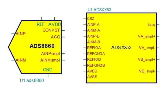
Figure 1 depicts the TINA-TI models of two popular high-precision SAR ADCs – the ADS8860 and the ADS8353. Both are 16-bit 1MSPS devices, but unlike the ADS8860, the ADS8353 contains two 1MSPS simultaneous-sampling ADCs. Both ADC models have several commonalities that make them functionally equivalent to each other.

Figure 1: TINA models of the ADS8860 and ADS8353 family of SAR ADCs


The inputs to each TINA model include the power supply, input, reference and “CONVST” or “CS” signals, which are defined in the datasheet. The outputs of each TINA model are “tacq” or “ACQ”, which indicate whether the ADC is in acquisition or conversion mode, and the “*smpl” signals represents the acquired input voltage values.

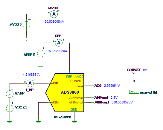
To see how well a SAR ADC TINA model correlates with the device datasheet, we can run a quick set of simulations using ideal input sources to drive the ADC model. For convenience, we use the ADS8860 TINA model as shown in Figure 2.

First we find the DC operating conditions of the circuit:

Figure 2: TINA schematic and simulation of DC operating conditions

When the ADC is not converting, it enters a “power-down” state, drawing about 50nA of current from AVDD. With ACQ high (3V logic), the ADC is in acquisition mode. Naturally, the sampled signal (AINPsmpl – AINMsmpl) is the same as the DC input (AINP – AINM) at 2.5V, and the supply current is about 30nA, indicating “power-down” mode operation.

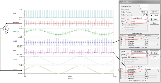
Next, we simulate the ADC’s dynamic behavior through a transient analysis of the circuit for a full-scale 40 kHz sinusoidal input. The average values of the supply and reference currents can be precisely determined by extracting the DC components of their Fourier Series expansions as shown in Figure 3.

(Click on image to enlarge.)

Figure 3: Transient analysis of ADS8860 showing RMS values of supply and REF input currents

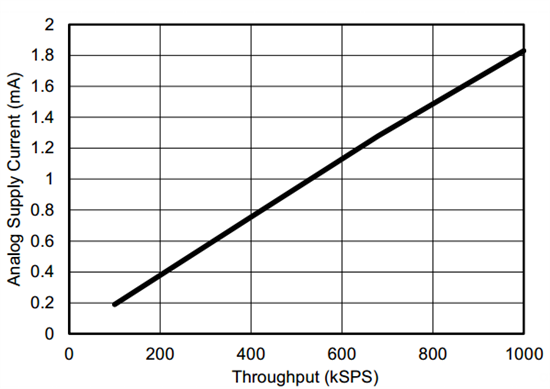
Once again we observe that the TINA model provides good approximations of the supply and reference input currents. Typical datasheet values are 1.8 mA and 300 uA respectively at 1 MSPS. Additionally, “Vsmpl” in Figure 3 clearly illustrates the sample-and-hold behavior that is fundamental to the SAR ADC architecture.

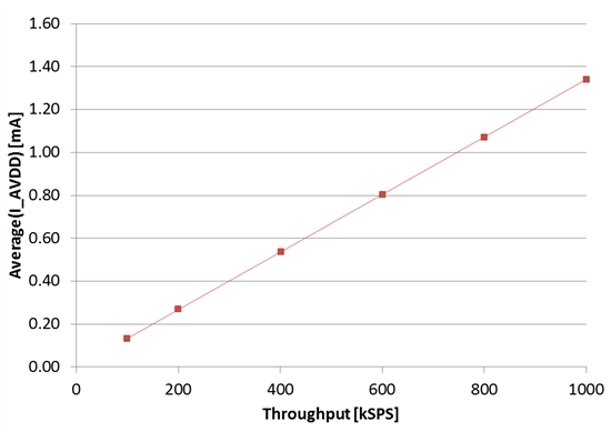
The technique illustrated in Figure 3 can be used to verify ADC power-scalability vs. sampling rate. Figure 4 depicts average IAVDD vs. sampling rate obtained by sweeping the CONVST frequency.

(Click on images to enlarge.)

Figure 4Comparison of TINA model estimate vs. datasheet plot of supply current vs. throughput

Figure 4Comparison of TINA model estimate vs. datasheet plot of supply current vs. throughput


The simulation differs from the datasheet in terms of the absolute current values at each sampling frequency, and this is probably because the TINA model may be based on IC simulation data vs. actual device test data that the datasheet uses. However, the simulation results do indicate a strong linear relationship between ADC supply current and sampling rate. 

In conclusion, the TINA model emulates a real SAR ADC in terms of static behavior and power scalability versus throughput.

Stay tuned for a follow-up blog post in which we examine how a SAR ADC model can be used to understand the effect of source impedance on ADC accuracy.

Related resources:

Read more about SAR ADCs on the Precision Hub.

See an overview of TINA TI. 

ADS8860 tools and software

ADS8353 tools and software

What are you sensing? Capacitive sensing for proximity detection and more

$
0
0

Capacitive sensing is becoming popular to replace optical detection methods for applications like proximity and gesture detection, material analysis, and liquid-level sensing. Capacitive sensing technology measures the capacitance resulting from change in dielectric material between two conducting plates.

Capacitance measurement basics

Capacitance is the ability of a capacitor to store an electrical charge. The capacitance (measured in Farads) of the common form―a parallel plate capacitor―consists of two conductor plates and is calculated by:

  • The parallel plate equation ignores the fringing effect due to the complexity of modeling the behavior but is a good approximation if the distance (d) between the plates is small compared to the other dimensions of the plates.
  • The fringing effect occurs near the edges of the plates, and depending on the application, can affect the accuracy of measurements from the system.
  • The density of the field lines in the fringe region is less than the density directly underneath the plates since the field strength is proportional to the density of the equipotential lines. This results in weaker field strength in the fringe region and a much smaller contribution to the total measured capacitance.

Figure 1 displays the electric fields’ path of a parallel plate capacitor.

Figure 1: Electric fields of a parallel plate capacitor

Applications

There are three common sensor topologies for capacitive sensing applications that utilize different working principles and target use cases. 

Figure 2: The three common sensor topologies

System-level integration with a capacitance-to-digital converter like the FDC1004 is fairly straightforward. The sensor, ground (GND) and shield electrodes can be any metal plate or foil. The FDC1004 is directly connected to a microcontroller or host processor via the I2C bus lines, as shown in Figure 3.

Figure 3: System-level block diagram

Theory of operation

The FDC1004’s basic operation of capacitive sensing implements a switched capacitor circuit to transfer charge from the sensor electrode to the sigma-delta ADC, as shown in Figure 4. A 25 kHz step waveform is driven on the sensor line for a particular duration of time to charge up the electrode. After a certain amount of time, the charge on the sensor is transferred to a sample-hold circuit for the sigma-delta ADC to convert the analog voltage into a digital signal. Once the ADC completes its conversion, the result is digitally filtered and corrected based on gain and offset calibrations.

Figure 4: FDC1004 capacitive sensing theory of operation

Use cases

There are several use cases where the FDC1004 provides significant advantages due to the device specifications and design features. These include:

  1. Independent channels
    1. Allows measurements from each channel to be unaffected by the other channels’ parasitic capacitance and noise.
    2. Enables the system to compensate for capacitance variances and offsets individually.
  2. Differential or ratiometric measurements
    1. Allows the system to track environmental changes to obtain accurate capacitance measurements from the sensor (minus the environmental factors).
    2. One channel (reference/calibration sensor) monitors changes in dielectric due to factors like temperature, humidity, material type, container stress, etc.
  3. Remote sensing
    1. Allows parasitic capacitance along the signal path from sensor to input of the FDC1004 to be compensated up to 100 pF.
  4. Time-varying offset measurements
    1. Similar to the differential concept but can track offsets that vary over time.
    2. Environmental factors that are not constant can be tracked and utilized to have a more accurate capacitance measurement.

Active shielding

Capacitive sensing with active shield drivers allows the capacitance measurements to be unaffected by any capacitance-to-ground interference along the signal path between the sensing device pins to the electrode sensor. The shield driver is an active signal output that is driven at the same voltage potential of the sensor input so there is no potential difference between the shield and sensor input.

There are several benefits to using a shield in capacitive sensing applications:

  1. Directs and focuses the sensing to a particular area
    1. Blocks fringing parasitic capacitances.
  2. Reduces environmental interferers
    1. Uses a shield wrapped around the sensor signal path.
    2. Environmental interferers include the human hand, radiated electromagnetic signals and noise from other electronic devices.
  3. Reduces and eliminates parasitic capacitances
    1. Helps mitigate fringing effects to PCB ground plane.
  4. Eliminates temperature variation effects on the ground plane
    1. PCB contracts and expands with temperature variations, creating capacitance variations that are not a constant offset.

Additional resources:

LDO and switcher solutions deliver cleaner, more efficient power for noise-sensitive Infotainment systems

$
0
0


Today infotainment systems are the personal electronics inside automobiles. Like personal electronics, automotive infotainment systems integrate many electronics in space constrained head units and instrument clusters to process various kinds of signals. One critical challenge for infotainment OEMs and suppliers designing these compact and feature-rich infotainment systems is delivering clean power rails to noise-sensitive applications such as audio codecs, gesture sensors, microprocessor digital radios, GPS, and Wi-Fi.  

One highly efficient way to provide cleaner power is using a linear regulator and switching regulator solution to transfer power from the automotive battery. Switching regulators are the most efficient method to convert DC power, but they are notorious for their ripples and EMI--especially in noise-sensitive infotainment applications. By adding a low-noise and high-PSRR LDO as a post-regulator, it creates a way to deliver a clean rail by isolating and reducing supply noise and by decreasing ripples over a wide range of frequencies.

One example of an LDO/switcher solution for noise-sensitive Infotainment systems isthe TPS54260-Q1, a 2.5A step-down switching regulator, and the LP5907-Q1, a 250mA low-noise and high-PSRR LDO. The TPS54260-Q1 is used to generate a lower rail voltage from the automotive battery. The LP5907-Q1 is then used to keep the noise down across a wide bandwidth and to reject ripples at various frequencies. The LP5907-Q1 provides a clean rail because of its low noise (10uVrms typical from 10 Hz to 100 kHz) and high PSRR from 1 Hz to 1 MHz (82dB typical at 1 kHz) with high tolerance over load variation. This solution can be used to generate a clean rail such as a 1.8V rail for Bluetooth and GPS and a 3.3V rail for audio codec, gesture sensors, microprocessor and Wi-Fi. Since the LP5907-Q1 doesn’t require a bypassing capacitor for noise reduction, the small solution size of the LP5907-Q1 also simplifies the design process and reduces the total solution size and BOM cost. 

LP5907-Q1 PSRR over various load conditions

What noise-sensitive infotainment designs could you use an LDO and switcher solution?


How to quickly tune your stepper motor

$
0
0

In our fast-paced world, there are many times we are tasked with having to make something work but don’t have time to learn the theory behind it. It’s important that it works but not as important why. This allows us to move on to the next task. In modern stepper motor drivers, tuning the motor for optimal current regulation can be one of those situations.

Recently, I’ve been asked why a stepper motor driver is misbehaving. The concern is that there are missing steps at low speed. The current waveform may jump up to one level and remain there until the steps catch up, or it may increase beyond the maximum chopping current. Typically the user has set mixed decay, but many devices use slow decay when the absolute value of the current is increasing.

Most often the distorted current waveform appears at holding or low speeds, where slow decay does not remove as much current as the driver inserted during the normal drive time. The problem is often worse as the motor voltage increases. The bottom image is an example of this loss of regulation at slow speed. The motor is driven at 200 steps per second with 1/8 microstep. The motor voltage is 12V.

In the top image, a new feature called adaptive decay is used to create the desired waveform at slow speeds. This new feature automatically adjusts the percentage of slow and fast decay to create a near optimal current waveform.

The bottom image shows a typical waveform using slow decay when the absolute value of the current is increasing and mixed decay (50% fast and 50% slow) when the absolute value of the current is decreasing. Note the missing steps as the current transitions from zero current, as highlighted in the yellow circle. This is due to the motor driver injecting more current during the drive state than is removed during the slow decay state. The missing steps can also be seen as the current begins to go negative.

Using these new features available, such as adaptive decay, you can quickly tune your stepper motor and move on to your next task.

For more information, please see check out:

DRV8846 samples

Watch my video for more on adaptive decay

See the DRV8846 in action using this 3D printer TI Designs reference design


Dynamic Voltage Scaling - Improve System Efficiency and Thermal Performance

$
0
0
The expression for power dissipation in a processor is P  f*V2. As system clock frequencies climb ever higher, nearing a state known as overclocking, efficiency is compromised and heat becomes a designer’s primary concern. Excess heat from...(read more)

Live Training Event: December 9th, 2014

Why functional safety certification is important for automotive applications

$
0
0

A few weeks ago, I happened to find myself at a local car dealership. After much negotiating, my oldest son had somehow convinced me that he was ready to own his own car. So here we were looking at several used cars – was the decision going to be something sporty, or staid but sturdy? At the top of my list was reliability and safety. While I’m not overly protective, I wanted to make sure that the car would keep him safe and wouldn’t leave him stranded because of a breakdown; after all, he had only been driving for a few months. Long story short, we picked the Subaru because it came as part of the dealer’s pre-certified program (and was a manual, which I could have fun with). Having experience with several used cars in my past, I know that it is sometimes hard to tell from the surface and the specs how reliable the car is really going to be. Knowing that an experienced expert mechanic had spent the time to inspect the car thoroughly and ensure it was good enough to warranty gave me a lot of comfort. After I bought the car, I did take it to my local mechanic to give it a once over, but he was not very familiar with this Subaru and told me not to worry as the pre-certified program at this dealer was well known and reliable.

 I know you are wondering how any of this has anything to do with functional safety. A few years ago when the ISO 26262 standard was newly introduced, we at TI decided to have the Hercules™ microcontrollers (MCUs) certified by an external assessment house for the simple reason that we believed having a “pre-certified” product would give our customers more confidence and lessen the burden of their certification work. If you are not familiar with ISO 26262, it is a standard for automotive passenger vehicle functional safety and specifies what is an acceptable failure rate (ASIL level) for a system based on the criteria of severity, exposure and controllability. Based on these criteria, it also prescribes a standard for how automotive systems must be developed to make sure all the appropriate checks and balances are put in place to avoid any “systematic” failures. Nearly all systems in the car today have some ASIL level associated with them.

Now going back to my car buying analogy the question one has to ask is — can someone without great familiarity with the innards of the complex MCUs in today’s vehicle really know with confidence that it meets their functional safety needs (the required ASIL level)? I’m not saying this is an impossible task, but it certainly is a difficult one. Building a robust, reliable and functionally safe system is difficult as it is; knowing that the components within that system have been built to a “pre-certified” standard will help considerably. As you build up your system level failure mode and effects analysis (FMEA) and start to break it down component by component, it helps if the failures in time (FIT) rate data are available for the component. It builds a lot of confidence if you know that this FIT rate data was checked by a certification expert and that the recommendations in the component safety manual have been reviewed and blessed by experts. Now you know if you follow the safety manual, your certification assessor will have an easier job.

For those customers to whom ISO 26262 is new, that’s another curve ball — what new collateral and evidence do they need to generate for certification? Well, you won’t need to generate this for any “pre-certified” component because that’s already been done! If your end system is going to be certified by a different assessor than the one we used for the certified Hercules TMS570LS12x/11x MCUs, they don’t need to become experts on the innards of the MCU as they know that someone credible has already looked at it and blessed it off. Just as if you took your pre-certified used car to your favorite mechanic, even when they are not familiar with the specific car, if they know that it was assessed by someone credible, they will feel a lot more confident that it meets the expected criteria!

Leave us a note and let us know—are you familiar with ISO 26262? How do you think a pre-certified component can help your product development and certification efforts?

DIY with TI: Staying on track with model train hobby

$
0
0

DIYer Wolfgang Wirth has a unique opportunity to show some creative things that TI devices can do at this month’s Modelleisenbahn Ausstellung (model train exhibition) in Ergolding, Germany.

 The hobbyist meticulously builds small-scale trucks and trains loaded with TI parts. His homemade miniature vehicles are designed to drive on tracks using magnets pulled by hidden wires and can even shoot video.

"I've installed many TI devices in model trains and trucks. I wanted to show that we can build anything with our ingenious TI devices," said Wolfgang, who has been a member of the Model Railway Club for 22 years and demonstrated his trucks at the show for the past decade.

"They are always very well-received by the visitors. Many travel from far away to visit our model railroad. We put great emphasis on the details," he said.

Wolfgang's trucks contain magnets in the steering column that follow an iron wire hidden under the street. There, a coil generates a magnetic field and can stop the vehicles when power is applied. 

His trucks use a variety of analog TI parts:

  • TPS63060 buck boost converter, which powers the DC/DC converter and motor.
  • A TPS61220 powers the camera, while another TPS61220 powers the transmitter.
  • A TPS61160 powers the orange marker lights that are on both sides of the truck and the trailer.
  • Each TPS61060 powers the headlights and the taillights.

 An on-vehicle camera has an analog composite output and transmits video to a receiver on a nearby TV. Wolfgang also hopes to add an MSP430 MCU to regulate the truck’s speed and provide indicators for direction and distance from other vehicles.

Wolfgang works as a technician in TI’s Advanced Low-Power Solutions (ALPS) business unit in Freising, Germany, making layouts for evaluation module (EVM) boards. He was the people’s choice winner of last month’s EMEA “DIY with TI” event in Freising based on employee votes.

"It was a great idea for TI employees to present their own creations," he said. "I'm going to continue to work on projects for the next DIY show."

As a future project, he hopes to find ways to charge the miniature vehicles wirelessly. For example, if the battery power gets low, the vehicles would automatically drive to a charging station.

Wolfgang has worked at TI since 1993 and in the Low Power DC-DC Converter group since 1999. To learn more about his projects, check out this website (in German).

Part 2: Two-Wire 4-20 mA Transmitters: Background and common issues

$
0
0

Part 1 of this blog series provided an overview of the operation and uses of two-wire 4-20 mA field sensor transmitters and provided a basic example system. The post also introduced the current transmitter compliance voltage, which when violated prevents the transmitter from properly regulating the current loop.

Today we’ll discuss the circuitry that regulates the output current of a two-wire transmitter by deriving the basic transfer function. Using the transfer function we will then explain another common application issue caused by connecting the transmitter return (IRET) to the loop supply ground (GND) or a fixed potential relative to the loop supply GND, as shown in Figure 1. The transmitter can’t regulate the output current (I) if IRET­ is connected to GND or another potential. It’s a very common question with a fairly simple solution. 

Figure 1: Two-wire transmitter with IRET incorrectly shorted to VLOOP GND

To understand why these issues occur, let’s use Figure 2 to take a closer look at the operation of the XTR116 with a focus on the IRET pin. As marked below, , the XTR116 IRET pin serves as the local, or 2-wire transmitter GND, for the sensor excitation and conditioning circuitry. The output voltages of VREG and VREF are referenced to IRET. The circuitry they power, including the bridge, instrumentation amplifier (INA), and internal op amp (U1), all return current to the IRET pin as defined in Equation 1. The IRET currents are marked in blue in Figure 2.

Figure 2: XTR116 4-20mA transmitter showing current flow


The IRET current sums with the bipolar transistor (BJT) current (IBJT), shown in orange, and flows through the 25 Ω sense resistor. The input current (IIN), shown in green, flows through the 2475 Ω sense resistor and then sums with IRET and IBJT to form the final 4-20 mA output current (IO), shown in red. The voltage drop across the 25 Ω resistor (VIRET­) connects to the op amp inverting input and drop across the 2475 Ω resistor (VIIN) connects to the non-inverting input. Therefore, the op amp will regulate IBJT such that VIRET and VIIN equal. Equation 2 uses Ohm’s law to determine the ratio of the currents flowing through the two resistors. 

Since IO equals the sum of IIN, IRET and IBJT, we can simplify Equation 2 as shown in Equation 3, which is the final transfer function. 

We can now define the voltage at IRET relative to the VLOOP GND. Figure 3 shows that VIRET depends on the 25 Ω internal resistor, the 250 Ω load resistor (RLOAD) and IO.

Figure 3: Determining the VIRET voltage relative to VLOOP GND

VIRET is defined in Equation 4.

VIRET is based on IO and therefore will change as the output current changes. This is shown in Figure 4 by measuring the VIRET voltage over the 4-20 mA IO span. 

Figure 4: Measuring VIRET while sweeping IO


Connecting IRET to VLOOP GND, as shown in Figure 1, forces VIRET to 0 V. Therefore, the transmitter can’t regulate the output current because the VIRET voltage is not allowed to move up and down with the output current.   

It is common to inadvertently connect IRET to VLOOP GND during testing or calibration/programming of the system. For example, making measurements with an oscilloscope on the transmitter side referenced to IRET, while making measurements on the loop side referenced to VLOOP GND, will short IRET and VLOOP GND together. This happens because the negative probe connections of the oscilloscope channels are internally connected, and also usually connected to earth GND.

The preferred solution is to reference all oscilloscope probes to VLOOP GND and use an additional oscilloscope channel to monitor the voltage at IRET. For measurements on the transmitter side, simply subtract the IRET voltage using the oscilloscope MATH function to obtain the measurement without shorting the IRET and VLOOP GND node.

In my next blog post we’ll talk about the current consumption limitations that affect the sensor and transmitter circuitry powered from VREG and VREF. An interesting solution will be presented to increase the power available to the sensor circuitry. 

Related TI Designs for 2-wire transmitters:

Related 3-wire blog posts from Kevin Duke:


Powering Bipolar Rails with Wide-VIN Fly-Buck Converter

$
0
0

I’m often asked by power system design engineers, how do you provide bipolar (positive and negative) voltage rails while keeping cost and complexity to a minimum? And at the same time, how should one deal with a variety of challenges―from galvanic isolation and widely-ranging input voltage to small solution size and electromagnetic compatibility (EMC)? Consider, for example, building and factory automation, test and measurement equipment, and isolated RS-485 and CAN transceivers in industrial communications applications.

Fly-buck Power Converter

Count on the Fly-BuckÔ topology for low-current auxiliary and bias rails, especially if both isolated and non-isolated outputs are required. Shown in Figure 1 and Figure 2 are Fly-Buck converter schematics based on the 100V LM5017 regulator.

Figure 1: Fly-Buck converter supplying non-isolated ±12V rails


Figure 2: Fly-Buck converter supplying isolated ±12V rails

 The circuit in Figure 1 provides non-isolated ±12V rails based on a buck-boost topology and unity turns ratio coupled inductor. The feedback loop regulates the net of VOUT+ and VOUT– for symmetric startup behavior. Conversely, the circuit in Figure 2 delivers isolated ±12V rails, apropos a need to reduce noise, break a ground loop, or provide user safety. A primary-side aux rail sends bias power to the LM5017 VCC input to minimize quiescent loss at high VIN. Bifilar winding of the split-rail secondaries balances winding parameters (such as DC resistance and leakage inductance) for better load regulation.

Powering Precision Analog Applications

Ideal for powering high performance analog applications where low noise and signal integrity are key (for example, PLLs, VCOs, bipolar op amps, A/D converters), Figure 3 details a Fly-buck converter with post-regulated ±12V rails. Here, the secondary-side slave outputs are derived from positive- and negative-output LDO post regulators. Both LDOs provide high DC accuracy over line and load as well as excellent AC performance in terms of PSRR and spectral noise density. The Fly-Buck converter in this example runs at 300kHz, and the LDOs’ wide-bandwidth PSRR attenuates the outputs’ switch-mode ripple and noise.

Figure 3: Fly-Buck converter supplying post-regulated ±12V rails for precision analog applications

 Indeed, many of the LDO control and protection features complement the Fly-Buck’s system-level performance. Examples of this are secondary-referenced ON/OFF, programmable soft-start, along with current limit and thermal shutdown protection functions. Also, as the Fly-Buck’s isolated output voltages hinge on the selected transformer turns ratio, post-regulation offers an easy way to fine-tune an output to a target voltage setpoint.

Fly-Buck Solution Versatility

A good understanding of Fly-Buck circuits should be established for all power engineers. With that in mind, I recently wrote an article, “Post Regulated Fly-Buck Powers Noise-sensitive Loads,” in Power Electronics Technology that delves into a low-noise solution for powering high-precision op amps and data converters. In summary, the Fly-Buck topology provides a cohesive feature set to meet a variety of power solution needs:

  • Reliable synchronous buck or buck-boost converter based design
  • Multiple regulator- or controller-based IC solutions depending on input voltage and output current specification
  • Well-proven constant on-time control technique with excellent transient dynamics
  • Straightforward BOM, no loop compensation or feedback opto-coupler components
  • Small-size magnetic component ideal for space-constrained designs
  • No primary-side voltage spike from transformer leakage inductance.

Visit ti.com/widevin to learn more about the Fly-Buck topology and its position within our purpose-dedicated portfolio of wide VIN controllers, converters and power modules.

Additional Resources:

  • Read “Post-regulated Fly-Buck powers noise-sensitive loads” in powerelectronics.com.
  • Check out the “Wide VIN power solutions for industrial automation” app note.
  • Refer to the “Wide VIN power management ICs simplify design, reduce BOM cost, and enhance reliability” whitepaper.
  • Review these designs from the TIDesigns reference design library:


New IR BoosterPack showcases remote control design with MSP430FR4x/FR2x MCUs

$
0
0

 Looking to create a solution for controlling your holiday lighting, television or air conditioning unit? Developing a universal remote control has never been easier!

The MSP430FR4x and MSP430FR2x microcontrollers are now available for order! These low-power MCUs feature up to 16 KB of embedded FRAM that can provide benefits from inherently protecting data to enabling data backup on power failure with its extremely fast and low-power writes. Beyond FRAM, the MSP430FR2x adds abundant IO and infrared modulation logic that minimizes the software development required for IR-based applications. The MSP430FR4x series even adds on a flexible and low-power segment LCD controller with software configurable pins and maintained contrast in low-power modes.

To get you started in minutes, we now are offering a new Launchpad Development Kit and BoosterPack Plug-in Module. The MSP430FR4133 LaunchPad enables low-cost development with the MSP430FR4133 microcontroller, on-board LCD controller, and the eZ-FET programmer/debugger. The infrared BoosterPack (BOOST-IR) enables developers to stack on an IR transceiver and keypad. These kits are also available at a discounted pricewhen you purchase the bundle (MSP-BNDLFR4133IR).

(Please visit the site to view this video)

The provided sample software enables a learn mode, for easily storing commands from another remote control. Another mode enables communication between two LaunchPads with IR BoosterPacks for developing both the IR transmitter and IR receiver in an application.

Ready to get started? Order the MSP-BNDL-FR4133IR today! For information on using the IR Modulation Logic on the MSP430FR4x and MSP430FR2x microcontrollers check out this application note.

Tune in next week for an overview of the latest TI Designs showcasing full system solutions from remote controls to thermostats that can benefit from infrared communication.

Giving the gift of wearables this holiday? Don’t forget to look at the battery charger!

$
0
0


The holidays are upon us and one of the hottest gifts this season will be wearables. Style and convenience is usually what people look for. But what about the battery? Charging a battery that is smaller than your thumb is totally different than charging a battery for smartphones or tablets. Wearable electronics are usually small in size such as smart watches, sports and fitness trackers and even clothing. Due to their physical constraints, the battery size and capacity is limited, even though longer battery run time becomes more critical for good user experience.

So, are you ready to design your power management solution to achieve the longest battery run time for your wearable devices? Selecting the right battery charger is almost the first thing you need to think about.

There are four main features an ideal charger IC for wearables should have:

  1. Small size. When the total device size is around 20mm x 20mm and the battery itself occupies more than half of it, a 4 mm x 4 mm charger IC is no longer suitable. The latest linear charger bq25100 offers a package size of only 1.6 mm by 0.9 mm and the total solution size is as small as 2.1 mm by 2.2 mm.
  2. Low maximum charging current. Over 90% of the wearable devices use a battery with the capacity less than 300 mAH and the state of art power density is 150 mAH/cm3. The bq25100 supports up to 250 mA battery charge current which is sufficient to charge almost all the wearable devices on the market today within two hours.
  3. High accuracy in termination current control. With the limitation in battery capacity, every mAh is important for the device run time. An accurate control at a low termination level prevents the battery from terminating early and therefore extends the battery run time. For a 41 mAH battery, the charge cycle with 1 mA termination current can bring an extra 2 mAH capacity than that with 4 mA termination current, which increases the usable battery capacity by 5%. The smaller the battery, the more critical the termination control. Think about a 20 mAH battery, if you cannot control the termination current below 5 mA, then you would lose more than 10% of the battery capacity even before you start using it. The bq25100 can accurately program and control the termination current down to 1 mA, which is the best across the industry today.
  4. Low battery leakage current. While we are maximizing the effective battery capacity, we should minimize unnecessary power consumption at the same time. Again, bq25100 has superior performance in this area. It has maximum 75 nA spec for battery leakage current from 0°C to 125°C and it would take 152.2 years to discharge a 100 mAH battery. Therefore, in reality the current is negligible as the self-discharge rate of the battery cell is much faster than that.

Now that you have the ideal charger, let’s discuss the charging process with some exciting new technologies like wireless charging.

The TIDA-00318 is a reference design circuit dedicated to wireless charging for wearables. It has the low power wireless receiver bq51003 and linear charger bq25100 on the same PCB with a total solution size of 5 mm x 15 mm. It is smaller than a fingertip and can be easily placed inside any wearable devices on the market. Paired with TI’s wireless transmitter IC bq500212A, it is a complete charging solution that you can apply to your device.

Is there a wearable device on your wish list this year? Please leave a comment and let me know!

Additional Resources:

  • For more details about our design for wearables, visit ti.com/Wearables
  • Order samples or evaluation module of the bq25100 linear charger
  • Order samples or evaluation module of the bq51003 wireless power receiver
  • Visit ti.com/wirelesspower for other wireless charging solutions that you can considered for low power applications

The Sixth Sense. What would you do with it?

$
0
0

Don’t you wish you had a sixth sense that let you see into the future – beyond what your current five senses allow?

While this is not possible (…quite yet! Who knows?), getting an early indication of what’s going on with our bodies is becoming a reality with medical sensor patches and wearable fitness technology. These devices are designed to monitor your body’s vital parameters such as temperature, hydration, pulse rate and more without tethering you to a bulky wired setup. While some solutions are pushing the limits on battery life, there are other innovative designs that are eliminating batteries completely. Even in the case of a battery-powered device, what happens if the battery runs out and the user still needs to pull the data off the device? This is an example where integrating Near Field Communication (NFC) into these designs can help. NFC technology can be used not only for data transfers but also to power these sensor patches when reading them using a reader device like an NFC-enabled smartphone.

Every year when I train for my half-marathons, I realize the importance of being properly hydrated. As anyone can tell you, proper hydration is critical to performance and health – not only for runners but also other athletes. So, what if I could have a virtually invisible, non-intrusive hydration sensor on my arm that I could read periodically by tapping my smartphone and find out my hydration level? Enough of bragging! But seriously, while my own training is not exhaustive enough to dehydrate me to dangerous levels, dehydration is a serious issue among athletes. A simple, low-cost hydration sensor patch can go a long way in timely detection of a problem.

Where am I going with this? Well, I am talking about using NFC-enabled sensor patches. NFC can bring value to these applications because it can be used to power sensors as well as for data transfers to a smartphone or another NFC-enabled device. Clearly the wireless data transfer can be achieved by other connectivity solutions such as Bluetooth®, Bluetooth low energy, Wi-Fi, etc., but NFC has unique advantages for these types of applications because of its low power consumption, passive (battery-less) operation and inherent security due to the proximity-based (a few centimeters) connectivity.

What’s fueling this trend is the proliferation of smartphones and integration of NFC in them. Smartphones are becoming a hub of health and fitness activity with their built-in sensors, but they can’t be in direct contact with the skin, so that’s where these medical patches (that can adhere to skin) can extend the functionality and feed data into the hub – our smartphones.

But the concept is not limited to medical applications. In industrial and  Internet of Things (IoT) segments, there are plenty of applications that can benefit from NFC capabilities. One such application is hermetically sealed (air-tight) glass encapsulated sensor nodes. Encapsulation allows it to be used in harsh environments and NFC can add passive (battery-less) operation and wireless connectivity.

Today, my team at TI is announcing a new addition to its NFC portfolio. The new RF430FRL152H NFC sensor transponder integrates an NFC interface with a fully programmable MSP430 MCU and other unique IP such as FRAM (non-volatile memory) for data storage, an ADC for analog sensors and I2C/SPI for digital sensors connectivity. Developers can use this highly integrated NFC transponder for quick and easy designs for their innovative applications that require sense-store-forward functionality.

Now the question is, what does this sixth sense mean to you and how would you use NFC to hone it?

SPICE it up: Why I like TINA-TI (Part 1)

$
0
0

TINA-TI is TI’s circuit design and SPICE simulation tool. I’m a big fan of the software, but it’s not just because I work at TI. I’ve used other SPICE-based simulation programs over the years. While most are fairly easy to use and robust, there are several reasons I prefer TINA-TI.

TINA-TI has a simple schematic editor, but it also includes powerful tools, like noise analysis, variance analysis and fast Fourier transform for distortion analysis. An added bonus: it’s free.

But one of the biggest advantages for me as an applications engineer is that TINA-TI has many of TI’s ICs already included and ready to use, including a pre-drawn and linked symbol. When I get a customer support request, I can open TINA-TI, grab the SPICE macromodel for the IC in question and start making initial simulations. This saves me tons of time, and if you’re designing with a new TI device, it’ll do the same for you.

Today, there are more than 650 operational amplifiers pre-loaded into TINA-TI. The software also comes pre-loaded with comparators, fully differential amplifiers, voltage regulators and more – plus a category for other devices. You can often design a whole system with the devices included in TINA-TI

But what happens if you don’t see the device you’re interested in listed in the “SPICE Macros” tab of the software? Don’t worry. Nearly all new TI amplifiers will have a completely assembled TINA-TI reference design available.

To see if a TINA-TI reference design is available for the device, just search for the part number on TI.com and visit the device page, which we call a product folder. Once you get to the device’s product folder, click on the “Tools & software” tab, as shown in Figure 1. You should see links for a macromodel and reference design in the models section. 

Figure 1: Tools & software tab of the LMH5401 product folder

From here, you can download the reference design file, which is a TINA-TI native file format and will automatically open if you have TINA-TI installed on your computer. If you prefer to use your own simulation software, you can also download the macromodel for use in other programs. The reference design will only work in TINA-TI, though.

Once you’ve downloaded the TINA-TI reference design model and have it running, as shown in Figure 2, you can perform a variety of proof-of-concept simulations. 

Figure 2: LMH5401 reference design circuit

For example, I always check DC operating conditions when looking at a circuit. I want to know:

  • Are the power supplies the right voltage? 
  • Are the input voltages in the correct range? 
  • Is the common mode voltage set right? 

A transient simulation will usually show these errors best, but you can also run a “Table of DC results” analysis to start. I usually skip the table and go straight for a transient simulation.

Figure 3 shows the results I got when I ran a transient simulation using the LMH5401 TINA-TI reference design. The LMH5401 is an 8-GHz, ultra-wideband fully differential amplifier (FDA) that can be used in AC- or DC-coupled applications that may require a single-ended-to-differential (SE-DE) conversion when driving an analog-to-digital converter (ADC).

Figure 3: Transient simulation results using the LMH5401 TINA-TI reference design

There are some interesting things going on in Figure 3. For example, why is the signal obvious when the amplifier is off, and why is the input signal impacted so much?

Check back on Friday, Dec. 19, for part 2 in this series, when I’ll answer these questions and walk you through some other helpful simulations.  

Additional resources:

Game-changing innovation captures top TI prize; TI fellows honored

$
0
0

LDC  1000 winning team

The world's first inductance-to-digital converter (LDC) is disruptive, differentiated and defies convention.

And it was developed by TI.

On Tuesday, Dec. 9, the company recognized the game-changing analog technology by naming the LDC1000 converter for inductive sensing applications as the winner of the new Jack Kilby Award of Innovation.

Hundreds of employees and leaders from around the world celebrated the award during the company's first-ever Innovation Ceremony.

"When we innovate well, we do well. Today is about celebrating some of the key technologists who are driving innovation," said Rich Templeton, TI's chairman, president and CEO. "Thank you for driving continuous innovation at TI."

Brian Crutcher, TI's executive vice president of Business Operations, and Kevin Ritchie, senior vice president of the Technology & Manufacturing Group (TMG), introduced the seven newly elected and re-elected 2015 TI Tech Ladder Fellowstwo from TMG and five from Business Operations. Brian also introduced the eight Jack Kilby Award of Innovation finalists, who were honored with applause during the program.

"Your vision, imagination and technical contributions are making a tremendous impact on the company and the world around us," Brian told the audience. "As we go into 2015, I ask that you continue to harness your energy, take it back into the businesses and where you are working, and challenge yourselves to come up with some of the greatest innovations we've seen and make an impact on Texas Instruments moving forward."

About the innovation award

Fifty-seven teams submitted projects for the Jack Kilby Award of Innovation, and TI's technical community then selected eight finalists, all from eight different organizations.

"This shows the diversity of innovation across the company," Brian said. "The finalists we are honoring today are enabling new products and opening up new market opportunities for TI."

LDC1000 core team members said they were thrilled and surprised to receive the award.

"Lots of people were involved in this effort," said George Reitsma, SMTS, analog designer and team lead based in Santa Clara, Calif. "Innovation is hard. It takes time to come up with the right product to meet our customers' needs."

George accepted an engraved Jack Kilby Award of Innovation trophy along with core team members Sumant Bapat and Rick Henderson.


About LDC1000


LDC1000 is the first generation of a new data converter category developed specifically to use inductors as sensors in an array of applications.  The Silicon Valley Analog (SVA) team developed the technology to make inductive sensing cost-efficient and simple, bringing its benefits to a large customer base.
   
LDC1000 has a large customer base today. Customers view inductive sensing as a disruptive alternative to entrenched sensing technologies in terms of flexibility, reliability and system cost.

"I am very proud of the LDC1000 team. I applaud their willingness to defy conventional approaches and develop a truly differentiated, game-changing device," said Dave Heacock, TI senior vice president over SVA. "Innovation is a top priority for all of us at TI, and I am excited this team was selected among the incredible group of finalists as an example of outstanding innovation."

Tech Ladder Fellows

TI leaders also honored seven newly elected or re-elected 2015 TI Tech Ladder Fellows during the Innovation Ceremony: Tom Bonifield (Analog Technology Development [ATD] in TMG), Luigi Colombo (ATD), Tim Anderson (Processors), Yevgen Barsukov (Power), Clive Bittlestone (Embedded Processing R&D Systems Lab), Mahesh Mehendale (MCU and Kilby Labs India) and Sandeep Oswal (Medical & High Reliability in High Performance Analog [HPA]).

TI's Fellow title represents one of the highest rungs on the TI Tech Ladder. It recognizes outstanding and consistent contributions by technical leaders who continuously drive highest levels of innovation and push new technical boundaries for the benefit of TI and its customers.

The election results for all TI Tech Ladder titles will be announced in February.

To see more photos from Tuesday's event, click here.

Viewing all 4543 articles
Browse latest View live


<script src="https://jsc.adskeeper.com/r/s/rssing.com.1596347.js" async> </script>