In the first two parts of my ADC accuracy series, I established the differences between resolution and accuracy for an analog-to-digital converter (ADC) and explained the factors that contribute to total unadjusted error (TUE) of the ADC. Most of these errors are static errors that can be calibrated under ambient conditions. System performance can continue to drift even after calibration, however, due to a change in temperature, which is common in many factory automation and control and other applications. Other factors such as aging of electronic components, humidity and pressure can also play a role in long-term performance drift.(read more)![]()
↧
ADC accuracy: Effect of temperature drift on ADC signal chain (Part 3)
↧
Power Tips: How to measure frequency response in isolated supplies
Do you dread compensating the feedback loop of your isolated power supplies? Where you choose to break the loop for your measurement will affect the difficulty of your task.
In Power Tip 76, we discussed how to easily select the compensation components around a TL431 circuit. While employing the equations in this Power Tip, it is crucial that you break the loop in a specific location. There are two locations at which we could choose to break the loop.
Most engineers are inclined to break the loop at the feedback resistor divider as shown in Figure 1. After all, this is what we do with non-isolated bucks. When we do this in isolated supplies, the inner loop becomes part of the plant and complicates the equations and the design procedure. When we break the loop at the divider, we must:
- Inspect the stability of the open inner loop.
- Then we must look at the closed loop response of this inner loop. The closed inner loop is the plant, which is controlled by the outer loop.
- Ensure stability by selecting the compensation components around the TL431 in the outer loop.

Figure 1. Breaking the loop at the feedback divider complicates the measurement procedure.
By breaking the loop as shown in Figure 2, we can stabilize the power supply in one easy step. Now the plant is defined as the transfer function from the output of the optocoupler to output of the power supply, and the two loops are included in our compensation rather than the plant. This allows us to use the simple equations described in Power Tip 76 to quickly choose the compensation components around the TL431.

Figure 2. Breaking the loop between the output and the entire TL431 circuit simplifies the measurement procedure.
Often, a 50 ohm resistor is incorporated into the circuit with the only purpose to provide a location for injecting a disturbance while measuring the loop. When placed in the location denoted by Figure 2, the impedance of this resistor will affect the performance of the power supply. The optocoupler current must flow through this resistor and will cause an error in regulation. If you place a resistor in this location, a zero Ohm resistor must be used. While performing a measurement of the loop, a 50 ohm resistor can be placed temporarily for injecting the disturbance. Afterwards, the zero Ohm resistor must be replaced.
We have numerous isolated supplies in our Power Lab library of reference designs. Here are a few examples which contain a zero Ohm place-holder resistor for measuring the feedback loop in the location shown by Figure 2:
- PMP9203– Universal AC Input 5V/2A USB Adaptor with Fixed Frequency Operation Reference Design: http://www.ti.com/tool/PMP9203
- PMP9204– Universal AC Input 5V/2A USB Adaptor with DCM/Valley-Switching and Opto Feedback Reference Design: http://www.ti.com/tool/PMP9204
- PMP9720– 48V-60Vdc Input, 12V/150W Active Clamp Forward - Reference Design: http://www.ti.com/tool/PMP9720
↧
↧
5 reasons TI supports Trade Promotion Authority
Congress is on the verge of introducing a bipartisan bill to reinstate Trade Promotion Authority (TPA), which allows Congress and the Administration to better collaborate on U.S. trade negotiations and implement resulting trade agreements. As a leading global semiconductor company with more than 100,000 customers worldwide, TI strongly supports TPA legislation. Here are five reasons why:
 1.) Open trade drives growth and helps TI reach our customers
Nearly 90 percent of TI’s revenue comes from overseas sales, with 61 percent of revenues from Asia and 18 percent from Europe.
Open trade is essential for TI to reach new customers emerging every day in countries around the world. It also allows our 100,000 customers reach new markets with their innovative products, creating even more growth opportunities for TI. In addition, open trade enables a robust supply chain that makes TI more competitive.
The journey of a TI chip demonstrates how important the free flow of goods and services is to American competitiveness. For example, we might design and manufacture a chip in Texas. Then, it could go to any one of our overseas AT sites for assembly/test and packaging. Next, it might travel to our product distribution center in Singapore where it is shipped to TI Korea to be sold to a Korean electronics manufacturer. The manufacturer might then sell it to any number of countries. By the time the chip reaches the end consumer in the final product, it could have traveled literally the distance around the world.
2.) The semiconductor industry is an excellent example of success through trade
In 2013, there were over 703 billion semiconductors sold in the world, or roughly 99 per person on the planet. U.S. semiconductor companies account for about half of the $336B world semiconductor market.[i]
Semiconductors have been one of the top three U.S. manufactured exports for the last fifteen years[ii]. The elimination of tariffs on semiconductors through trade agreements, such as the Information Technology Agreement in 1996, played an important role in expanding global markets for U.S. semiconductor firms, and has benefitted consumers and workers around the globe.
As a company and an industry, we have a unique and positive story to tell about international trade.
3.) TPA is necessary to conclude and secure a vote on new trade agreements
TPA facilitates open trade policies and new agreements to access more customers for goods and services. TPA will enable U.S. negotiators to conclude and Congress to implement new trade agreements such as the Trans-Pacific Partnership (TPP) and the Transatlantic Investment Partnership (T-TIP) that address 21st century trade barriers and provide U.S. companies with greater access to key markets around the world, boosting growth and job creation.
Trade is not a zero sum game. TPP would open markets and increase trade among all the 12 countries around the Pacific Ocean that account for 40 percent of global GDP[iii] and 15 percent of global trade[iv]. The agreement benefits TI and other high-tech companies by increasing protection of intellectual property, addressing encryption and standards, and improving regulatory transparency.
Semiconductor and component exports from Texas to the five TPP countries without U.S. free trade agreements (Brunei, Japan, Malaysia, New Zealand, and Vietnam) accounted for $754M in 2013.[v]
The U.S. and the European Union represent nearly half of global GDP and 30 percent of goods trade[vi]. The T-TIP agreement will promote regulatory cooperation and protect cross-border data flows, beneficial provisions for TI and other U.S. firms.
The legislation outlines clear objectives that Congress sets for U.S. negotiators. TPA allows a completed trade agreement to receive a yes-or-no vote in Congress, with no amendments that would alter a carefully negotiated deal.
Every President since the 1930s until 2007 has had authority from Congress to negotiate trade agreements. Congress retains final authority to approve or reject trade agreements under TPA.
4.) 21st century trade barriers require new legal tools
TPA was last passed in 2002 and expired in 2007. Since that time technologies have changed significantly and the economy has become increasingly global. We need updated legislation to address emerging 21st century trade barriers such as intellectual property, technical standards, encryption, cross-border data flow, and forced technology transfer.
5.) TPA is a bipartisan issue
In his State of the Union Address, President Obama identified passage of TPA as a top priority, and key Republican and Democratic leaders in Congress also understand its importance. TPA is something that can get done this year.
TI is actively working to secure a favorable vote on the bill, sharing our perspective with the Members of Congress who represent our sites. We are amplifying our support through trade associations, as well as traditional and social media.
TI is a member of the Trade Benefits America Coalition, and is working closely with our trade associations such as the Semiconductor Industry Association, the Information Technology Industry Council, the Business Roundtable and National Association of Manufacturers, who are all aligned in support of the bill.
At a time where agreement on many other issues is rare, TPA provides an opportunity for Democrats and Republicans to work together. It’s time for Congress to act on TPA.
[i] Semiconductor Industry Association
[ii] U.S. International Trade Commission
[iii] U.S. Trade Representative
[iv] Business Roundtable
[v] Business Roundtable
[vi] U.S. Trade Representative and European Commission
↧
Driving Innovation: In the right lane to making the drive safer, greener and more fun
Ever since the introduction of the automobile, driving has always been an experience. Luckily for everyone, TI is dedicated to making that drive safer, greener and more fun. From headlights to taillights and all the systems in between, we offer a wide range of innovative technologies for the modern vehicle. With TI’s full portfolio of components, including solutions in infotainment, critical active and passive safety and advanced driver assistance systems (ADAS) to emerging solutions for hybrid/electric power train systems and wireless connectivity technology, TI is changing the way the industry thinks of automotive innovation.
Design engineers can create the latest solutions to effectively address the next wave of automotive features, including the connected car, safety, infotainment, and, ultimately, autonomous vehicles. This month, TI will be showcasing how we drive innovation across Analog, Embedded Processing and DLP® Products technologies. Each day we will be updating this blog post with additional blog posts that cover all of TI’s offerings in automotive innovation. Be sure to follow along on social media using the hashtag #DriveInnovation.

If you have questions on TI's portfolio of automotive technology leave a comment below - We'd love to hear from you.
To learn more about how TI drives Innovation, check out these other Automotive Innovation blog posts:
↧
Doing the math: The inside story of the “Analog Engineer’s Pocket Reference”
As an analog applications engineer, much of my problem-solving involves recommending application circuits for customers to use as subcircuits in their overall product design. Thus, I understand the need for standard values, formulas, printed circuit board (PCB) characteristics and shortcuts for predicting performance.
A colleague of mine, Tim Green, has about 32 years of experience, of which 16 are in board-/system-level design. When I asked him how he handled these common design aids, he opened his file cabinet and pulled out a folder stuffed full of dog-eared and well-worn papers he’d collected over the years of his favorite design collateral. One of the things that fell out was a small 25-page booklet called “The Burr-Brown Electronic Engineers Pocket Reference,” published in 1994.
That booklet was the motivation for Tim and I to modernize, simplify, organize and electronically publicize the new Texas Instruments “Analog Engineer’s Pocket Reference” (Figure 1).

Figure 1: TI’s new “Analog Engineer’s Pocket Reference” inspired by a 1994 Burr-Brown booklet
One general problem with pocket references is that you have to be really familiar with them. In other words, when confronted with a difficult problem, you might resort to a Web search before using the pocket reference if you don’t know that the answer is in the pocket reference.
So in order to help familiarize you with the new TI pocket reference, I have put together some questions. Try to answer the questions using the pocket reference and you will gain a much deeper understanding of the book’s powerful content.
Question 1 (hint: Analog section):
Referring to the circuit below, what is the phase shift at 100kHz?

Question 2 (hint: Amplifier section):
Referring to the circuit below, what is the rise time for the 20mVpp step wave input? Note that this is a small signal step and the OPA209 has a gain bandwidth product (GBW) of 18MHz (data sheet SBOS426).

Question 3 (hint: Amplifier section):
What is the noise spectral density of a 10kΩ resistor?
Question 4 (hint: Amplifier section):
Given the transient closed-loop waveform shown below, what is the loop gain phase margin?

Question 5 (hint: PCB and Wire section):
Referring to the figure below, what type of package is this?

Question 6 (hint: Sensor section):
What is the resistance for a PT100 resistance temperature detectors (RTD) at 100℃? Assume that the RTD adheres to the ITS-90 standard.
Question 7 (hint: A/D Converter section):
Calculate the effective number of bits (ENOB) for an analog-to-digital (A/D) converter assuming signal-to-noise and distortion (SINAD) (dB) of 75dB.
For the benefit of those who are still working through the problems, please do not post answers in the comments. I will post the answers next week. Good luck!
Additional resources:
Download the Analog Engineer’s Pocket Reference to get often-used A/D conversion formulas in one place.
↧
↧
Making a plant watering reminder system with LaunchPad & Energia!
Don't you hate it when your plant forgets to remind you every time it needs water? Yeah, me too...
Fortunately enough, there are tools available that make it easy for developers to rapidly prototype their own solution using the TI LaunchPad development tools, Energia software & Grove sensor modules from SeeedStudio.
In this tutorial, I'll walk you through on how to create your very own internet-connected flower pot moisture sensor that will send you a text message when your plant needs water!
Here's what you'll need
- MSP-EXP430F5529LP LaunchPad (Other Energia-enabled LaunchPad kits can also be used)
- CC3100BOOST WiFi BoosterPack
- from SeeedStudio &
Grove Moisture Sensor from SeeedStudio
- NOTE: The CC3200 WiFi LaunchPad can also be used in place of the LaunchPad + CC3100 WiFi BoosterPack above
Here's a quick video on how to plug everything together! In this tutorial, we will have the Grove Moisture sensor connected to pin 23 of the LaunchPad:
(Please visit the site to view this video)
Reading the analog Moisture sensor
First thing's first - we need to download Energia @ www.energia.nu
Now that our hardware is ready to go, let's switch our focus to the software. In this case, we will be using Energia to write our firmware. Energia offers a simple API for reading analog inputs, called analogRead() that we will be using. Fortunately enough, Energia offers a nice example that we can use to simply print out our raw analog readings to its built-in Serial Monitor.
You can find this example at FILE > EXAMPLES > BASIC > ANALOGREADSERIAL
Next, we need to tell Energia which board we want to compile this code to. We can select the appropriate LaunchPad board by navigating to: TOOLS > BOARD > [Select your board. In my case, I am using MSP430F5529 LaunchPad (25MHz)]
We will also need to tell Energia which Serial/COM port our LaunchPad is connected to. typically it is the last one on the list available at TOOLS > SERIAL PORT > [Select your serial port. Check your device manager if you are unsure]
Here's a quick video on how to use Energia to read the analog values coming from your moisture sensor:
(Please visit the site to view this video)
Using Temboo to interact with various cloud services
At this point, our hardware should be reading moisture sensor data from the Grove moisture sensor. Now, that we have this baseline functionality, let's figure out how to interact with the cloud to trigger a text message. To do this, we are going to leverage Temboo.
You can learn more about Temboo at www.temboo.com/hardware/ti
You will need to sign up for a Temboo account. We are also going to need a Twilio account, since this is the web service that we will use to trigger our text message. You can get one at www.twilio.com.
TI has collaborated with Temboo to provide a seamless development experience for enabling internet-connected hardware to interact with various websites & web services. In this case, we are going to use Temboo to generate Energia code that will allow our LaunchPad to send a text message using the Twilio web service.
Temboo makes it really easy to generate the right Energia code by simply asking for a few parameters from the developer. Once the Energia code is generated, we can simply copy & paste the code into Energia to be compiled & flashed into the LaunchPad.
Here's a video that demonstrates how easy it is to generate Energia code:
(Please visit the site to view this video)
Triggering a text message with Temboo & Twilio
Now that we have the Temboo-generated code, we can copy-and-paste it into Energia. Temboo generates both an application sketch as well as a TembooAccount.h file, which includes all of our Temboo and WiFi credentials. We can copy and paste both of these files into Energia& can flash this into the LaunchPad. At this point, our LaunchPad will trigger a text message every 30 seconds. Without writing any code, Temboo makes it really easy to enable our LaunchPad to interact with various cloud services; in this case, Twilio for triggering SMS messages.
Here's a video of our LaunchPad sending a text message with the help of Temboo and Twilio:
(Please visit the site to view this video)
Triggering a text message only when sensor values exceed a threshold
At this point, we have all of the required components for pulling together our application - we are successfully reading moisture sensor values from the Grove Base BoosterPack and Moisture sensor AND we are able to successfully send text messages with the help of Temboo and Twilio. Now, we need to tie these pieces together. In short, all we really need to do is encapsulate the Temboo-generated code in an if-statement. That way, we will only trigger off the text message when the if-statement condition is met. In our case,we only want to trigger the text message when the analogRead(23) function returns a value that is passed a certain threshold. In our case, we only want to send a text message when the moisture sensor returns a reading of 0, indicating that no water is present.
Here's a video of how we combined the two code examples to build our complete application:
(Please visit the site to view this video)
AND THAT'S A WRAP!
With this tutorial, hopefully you were able to see how simple it can be to use modular hardware to rapidly prototype a complete Internet of Things application using easy-to-use and intuitive software tools. With these components, it becomes much simpler to enable real-world hardware to interact with the cloud.
So go ahead and get started!
- www.energia.nu
- www.temboo.com/hardware/ti
- Seeed Studio Grove Starter Kit for LaunchPad
- www.ti.com/launchpad
↧
4, 3, 2, 1 Countdown to MWC 2015
Well we have marked the passing of the month of February, yet this relentless cold and snow in the US makes one wonder, will the winter of 2015 ever be over! Ah, but we are on the eve of Mobile World Congress (MWC) 2015, so spring must truly be around the corner. While the Barcelona destination certainly helps, the exciting energy at MWC always seems to deliver news and progress to the ever changing world of the mobile infrastructure.
So what will we be the buzz at the show this week? Certainly ONE of the main challenges providers are trying to overcome is not new: despite the ever increasing demand for wireless data usage, the amount of spectrum is limited. How do we as an industry squeeze more data through a finite pipe?
Well, we have a preview about how that problem is being tackled from TWO key market players; wireless operator, T-Mobile and wireless equipment manufacturer, Nokia Networks, via their pre-MWC announcement , unveiling a solution called Licensed Assisted Access (LAA).
This solution is comprised of THREE key elements:
- While not a new idea, the concept of leveraging unlicensed spectrum to augment existing wireless licenses, and providing offload of data traffic has been debated. To date, one of the most common technologies suggested for using this availability of unlicensed spectrum has been wi-fi.
- Anticipating the need for additional spectrum, the LTE-Advanced (LTE-A) or 3GPP Release 10 standard has a feature called carrier aggregation that enables operators to leverage two disparate slices of licensed spectrum together. This creates the effective bandwidth of a single wider band, providing higher bandwidth downlinks and hence more data to users.
- Subsequently, the solution leverages the LTE carrier aggregation specification, but with both unlicensed and licensed spectrum to form sort of a hybrid aggregated band. This is all in the form of a pre-standard concept called LAA (or LTE-U).
And I find all of this very exciting! Why? Because as a member of a team delivering enabling technology, wireless base station SoCs, I know we need to be patient to see the fruits of our labor. So it is no surprise that the recent announcements about pending LTE-A, LTE-U and LAA deployments are perfect examples of where our wireless team’s “products” have come to fruition to solve a common problem.
Here are FOUR specifics:
- 3GPP STANDARDS PARTICIPATION: TI has long been an active participant in the innovation and development of the 3GPP standards, notably the LTE-A specification including significant feature carrier aggregation, a key element to enabling this LAA to achieve the desired bandwidth. More details on LTE-A and carrier aggregation is shared by one TI’s 3GPP contributors in an earlier blog.
- HIGHEST SOC PERFORMANCE: For years now, our KeyStone architecture has been the foundation for our high performance, power optimized wireless SoCs, believing in the need for planning SoC performance for what was “future” feature such as carrier aggregation, LTE-A. The TCI6636K2H, selected Best Embedded Processor of the year by the Linley group, and the TCI6630K2L are both examples that support LTE-A Carrier Aggregation and LAA/LTE-U, with the TCI6636K2H deploying these features in customer solutions today.
- FLEXIBLE SOFTWARE: Getting our customers, the wireless equipment suppliers to market quickly, enabling them to focus of product differentiation without sacrificing LTE performance is what our Basestation SoftwarePac is all about. And, the recent version of this SoftwarePac now supports carrier aggregation!
- CUSTOMER ADOPTION: And finally, wireless solutions equipment providers, leveraging our products such as Nokia Networks to get this cutting edge technology to market.
The supply chain in action! I would love to hear your thoughts on this topic, or anything else you find exciting at MWC.

↧
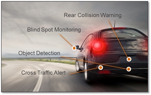
Eyes in the back of your head: Automotive radar goes mainstream

Do you remember when you were a kid and it seemed like your mother always could see what you were doing, so much so that it seemed like she had eyes in the back of her head? There are several situations that we encounter on a daily basis where actually having eyes to see things in places other than right in front of us would be extremely useful. One of these situations is behind the wheel in the driver’s seat of an automobile. I recently saw a car advertisement on TV that describes the roadway as "360 degrees of chaos." This ad describes many of the hazards that exist around an automobile during a normal driving experience and promotes the latest radar-based advanced driver assistance systems (ADAS) that aid in detecting these hazards and obstacles. One of the most interesting aspects about this commercial is that it wasn’t for a high-priced luxury automobile, but for a standard mid-sized family sedan. Features like blind spot monitoring, cross traffic alert, obstacle detection and collision-warning systems have been around for a number of years; however, they have only been deployed in limited numbers and available only in high-end vehicles.
Recent improvements in the amount of integration possible in these 24-GHz radar systems have enabled these features to be offered in more mainstream automobiles. One key component at the heart of these systems is the digital signal processor (DSP) that performs all the math-intensive computations necessary to process the data received from the radar sensors. One way that TI is enabling this high level of integration is with the C2000™ Delfino™ F28377D microcontroller. This MCUs provide the necessary blend of integrated analog and control peripherals coupled to a real-time DSP engine designed for applications requiring heavy signal processing. There are up to 800 MIPS of floating-point DSP performance with the available dual C28x CPUs and dual CLA real-time co-processors. The C28x’s integrated Trigonometric Math Unit (TMU) and Viterbi Complex Unit (VCU) enhance the performance of the C28x CPU by reducing the number of instruction cycles necessary to perform calculations commonly made in ADAS applications.
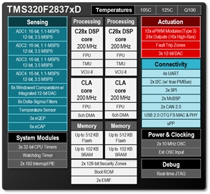
The C2000 MCU’s highly integrated on-chip peripherals are highly optimized for real-time controls tasks. Fast and precise data acquisition from radar sensors is made possible with four independent analog to digital converters. These ADCs have selectable 16-bit and 12-bit modes and can achieve up to 3.5 mega samples per second. Radar stimulus can be provided with the enhanced PWM modules that offer sophisticated shadowing, synchronization, edge positioning and trip logic in addition to precise duty cycle edge placement. 12-bit buffered DACs are also available to provide enhanced control capabilities.
C2000 real-time-control MCUs bring the power of a DSP into an MCU architecture that is designed to meet the requirements of the automotive and transportation industries. For more information, visit the C2000 MCU transportation application webpage.
To learn more about how TI drives Innovation, check out these other Automotive Innovation blog posts:
↧
TI named top company for executive women
When I began my career as an intern in Human Resources 15 years ago, I knew very little about what it truly meant to be a TIer.
My appreciation for this beloved TI nickname has grown alongside my unforgettable career journey – a voyage that has...(read more)![]()
↧
↧
Delta-sigma ADC basics: Walking around the delta-sigma blocks
In the first two posts of the delta-sigma (ΔΣ)analog-to-digital converter (ADC) basics blog series, we have discussed the two basic building blocks used in ΔΣ ADCs: the modulator and the digital filter. You’ll encounter many other integrated circuits as you work with these devices, however. The available functional blocks and the many variations of each one are why there are so many different ΔΣ ADCs customized to particular applications.
In this post, I’ll briefly look at many of these functions and talk about how they fit into different applications. Let’s imagine each type of ΔΣ ADC as a neighborhood, and walk around some block diagrams, beginning in a sparsely populated rural area.
ADS1252 (rural)
Figure 1 shows the block diagram of the ADS1252ΔΣ ADC. The modulator and digital filter are the essential parts. Let’s look at the other represented blocks.

Figure 1: Block diagram of the ADS1252ΔΣ ADC
Interface and control logic
The interface and control logic blocks are common to all ΔΣ ADCs and represent all that is needed to complete the device. In the case of the ADS1252, a simple two-pin interface (SCLK and DOUT/DRDY) provides an output of the conversion results. This basic interface is what allows the ADS1252 to quickly start up and provide data from a wide variety of sensors. Meanwhile, the logic controls can synchronize conversions with multiple devices, notify you when a data conversion is complete and power down the ADC when not in use.
Rural areas are usually quiet and devoid of the daily hustle-and-bustle of urban life. Similarly, the ADS1252 is an unsophisticated and simple ΔΣ ADC, that can be used for process control applications and thermocouple measurements.
Now that you’re familiar with the basic ΔΣ ADC block diagram, let’s walk toward a nearby town …
ADS1259 (suburb)
On our stroll into town, we pass through a suburb. The houses are getting closer and closer together, although each one is still unique. It is here where we encounterthe ADS1259, shown in Figure 2.Check out all the blocks!

Figure 2: Block diagram of the ADS1259ΔΣ ADC
Internal reference
All ΔΣ ADCs require a voltage reference to define the full-scale range of the modulator. The ADS1259 block diagram shows an integrated 2.5V reference. In most applications, the integrated reference provides sufficient input range and noise performance (more on reference noise in a future blog post); however, input pins (VREFP and VREFN) still allow for the application of an external reference. An external reference is usually required when performing ratiometric measurements (more on ratiometric measurements in a future post).
Internal oscillator (clock generator)
All ΔΣ ADCs use a clock source to determine the modulator’s sampling rate. The ADS1259’s clock-generator block provides a clock without any external components; however, attaching an external crystal may help stabilize the modulator clock or generate a different modulator clock frequency, affecting the modulator sampling rate and output data rates.
While the suburban homes are still fairly dispersed, we simply haven’t the time to see everything in the area. Similarly, the ADS1259 has many other features that I won’t cover in this post; you can learn more about them here. Devices like the ADS1259 integrate many useful circuits into the ADC to significantly reduce the amount of printed circuit board (PCB) area and cost required to fit a ΔΣ ADC into a system. However, even with the high level of integration, we are left with plenty of flexibility to use this device in many different applications, including high-resolution weigh scales. The facade of the ADS1259 might not make it obvious, but it is one of the lowest-noise, highest-resolution ΔΣ ADCs used for DC measurements.
ADS1220 (urban)
We finally reach town and find this urban area to be a little more crowded, much like the ADS1220 block diagram shown in Figure 3.

Figure 3: Block diagram of the ADS1220ΔΣ ADC
Multiplexer
The multiplexer increases the number of ADC inputs and allows for measurements of multiple sensor signals consecutively. To measure multiple sensors simultaneously, multiple ΔΣ ADCs or multiple ΔΣ modulators would be necessary (see the ADS1278 block diagram for an example). There are also ΔΣ ADCs with much larger channel counts (see the ADS1258 block diagram).
Programmable gain amplifier (PGA)
A PGA placed before the ΔΣ modulator amplifies small signals, providing higher resolution (more on gain and resolution in a future post).
IDACs
You can use programmable current digital-to-analog converter (IDAC) sources to excite and measure most resistive-type sensors such as thermistors, resistance temperature detectors (RTDs) and strain gauges.
You can find almost anything in a crowded city; likewise, the ADS1220 contains nearly everything you’d need to interface directly to a sensor. This ADC is well suited for instrumentation using temperature or bridge (strain) sensors and is ideal for space-constrained or low-power designs like temperature and pressure transmitters.
The road goes on and on, but it is here where our journey ends; we’ll part ways (for now). I hope you are more comfortable navigating ΔΣ ADC block diagrams. If you’d like for me to cover a particular functional block I didn’t include, let me know in the comments below.
For more in-depth information, see the following resources:
- Use the Precision ADC parametric search tool to search for the right ADC for your application.
- Browse questions about TI’s precision ADC applications in the TI E2E™ Community Precision Data Converters forum.
- See the ADS1220 delta-sigma ADC in these precision designs in the TI Designs reference design library:
- Temperature Sensor Interface Module for Programmable Logic Controllers (TIDA-00018)
- Small Form Factor, 2-Wire 4 to 20mA Current Loop RTD Temperature Transmitter Reference Design (TIDA-00165)
↧
Measuring noise requirements for ADC power supplies
In my previous blog, “Measuring PSR in an ADC”, I developed a complete PSR characterization procedure for a pipeline analog-to-digital converter (ADC) with low voltage differential signaling (LVDS) output and the methodology necessary to develop a power-supply specification for the maximum allowable ripple on the power-supply pins.
In this second installment of the blog, I will look at DC/DC converters both for the analog Vdd (AVDD) and the digital Vdd (DVDD) power supply. Understanding how ADC power-supply pins react to DC/DC converters is critical, since DC/DC converters are part of most (if not all) powering schemes due to their high power efficiencies.
DC/DC converter efficiency can be in the mid-90 percent, providing the most power-efficient solution where power needs to be provided. DC-DC converters have two main components to their internal power dissipation: static power dissipation and dynamic power dissipation
Static power dissipation corresponds to the energy needed to implement the functionality of the chip and is normally , where IQ is the quiescent current and VS the supply voltage.
Dynamic power dissipation corresponds to the energy needed to transmit the desired power to the load. In DC-DC converters, the main contributors are energy lost:
- During the switching transition.
- Driving the output metal-oxide semiconductor field-effect transistor (MOSFET).
- In the MOSFET due to the internal series resistance.
- In the inductor used to average the output voltage resulting in the DC voltage.
Figure 1 shows the efficiency curve for DC-DC converters.


Figure 1: (a) TPS54120 DC/DC (b) TPS62080 DC/DC
efficiency curve efficiency curve
Notice that the efficiency at the light load current drops dramatically and can indeed be worse than the efficiency of a linear regulator operating with a light load. As such DC/DC converters are always better when loaded optimally or with a load varying within a specified range to ensure efficiency. The highest efficiency for the TPS54120 is achieved above 500mA (>85 percent); for the TPS62080, it is from 300mA to 800mA (>90 percent).
I will not spend more time on the selection of DC/DC converters, as the best solution will depend on efficiency, cost, printed circuit board (PCB) area occupied versus available, possible electromagnetic interference, etc. …
For this analysis, I will use the TPS54120 and TPS62080 as example of the power-supply solution to evaluate the impact of different switching frequencies. The TPS54120 is switching at 480kHz typical and the TPS62080 at 1.5MHz. The TPS54120 is a dual-output device with one output being a low-noise, low-dropout linear regulator (LDO) and one output being a DC/DC converter. The TPS62080 is a 1.2A high-efficiency step-down converter.
The TPS54120 is an extremely versatile device with a small PCB footprint that can be used as either a high-efficiency LDO (DC/DC and LDO used in series); see figure 2(a) or a power-tree optimizer (DC/DC and LDO used independently); see figure 2(b).

A) {12V to 1.8V at 1A; Efficiency ~ 70%}

B) {2.3V to 1.2V at 3A; EfficiencyDC-DC ~ 83%}
{1.3V to 1.8V at 1A; EfficiencyLDO = 78.3%}
Figure 2: (a) High-efficiency LDO, (b) Power-tree optimizer configurations
Under no-load conditions, the time-domain response of the TPS54120 exhibits a 600µVPP ripple as shown in Figure 3.

Figure 3: TPS54120 DC/DC converter time-domain ripple
This time-domain ripple can be converted to a frequency-domain plot; see Figure 4.

Figure 4: TPS54120 DC/DC converter frequency-domain response
The TPS62080 is a 1.5MHz, 1.2A step down DC/DC converter. Figure 5 illustrates its time-domain no-load response. Note that this response exhibits an 8mVPP ripple. This response is the TPS62080 snooze mode and will be similar to the TPS54120 DC/DC response once a load is attached to its output.

Figure 5: TPS62080 time-domain no-load response
The fast Fourier transform (FFT) of Figure 5 is shown in Figure 6.

Figure 6: TPS62080 no-load FFT
Both Figure 4 and 6 show the components that the ADC will need to be rejected by the ADC. These are not the best DC/DC converters from an efficiency standpoint for a 200mA load such as the one the ADC3444 will exhibit, but it is understood that the load would be shared with additional components on board. Figure 7 shows the TPS54120 DC/DC converter FFTs for various loads. In this figure, you can notice the increased amplitude of both the fundamental and its harmonics as the load is heavier. These degradations will find their way in the output spectrum of the ADC for a steady additional DC/DC converter load, other than that presented by the ADC. If this additional load were to vary, you would then have to deal with a modulation of the amplitude of the DC/DC converter as well.

Figure 7: TPS54120 FFT for various loads
I selected the TPS54120 and the TPS62080 due to their availability, allowing the evaluation of the ADC3444 with two very different switching frequencies (480kHz and 1.5MHz).
Looking first at the DVDD supply of the ADC3444 from the previous blogs, see “Measuring PSR in an ADC”, we know that the maximum allowable ripple at the DVDD pin is ~15mVPP. Having a ripple below this value will ensure that not tone greater than -95dBFS will be present on the ADC FFT.
My evaluation is based on the block diagram shown in Figure 8. In this figure, you can notice that the power supply source is a battery. The use of a battery guarantees that the only source of power-supply switching-noise is originating in the DC/DC converter. On the DVDD supply, under test, we inserted the DC/DC converter without any post-filtering, only maintaining the four 0.22µF capacitor at each ADC3444 DVDD pins. The AVDD supply pin is powered of the same battery, but this time followed by a low-noise LDO, to ensure regulation at the appropriate voltage, but also provide an excellent rejection to any external switching noise and low thermal noise to the AVDD pins while providing the low impedance to the AVDD supply that is expected from a good power supply.

Figure 8: ADC3444 DVDD test configuration
(Note: No ferrite bead was used as we are evaluating ADC3444 power-supply rejection ratio [PSRR] performance)
The ADC FFT results for both the TPS54120 DC-DC are shown in figure 9 below.


Figure 9: (a) ADC3444 reference plot; (b) ADC3444 FFT with TPS54120 as DVDD supply
We now have confirmation that our earlier calculation, from my “Measuring PSR in an ADC” post that a ripple below 600µVPP, the DVDD supply does not have any tone at the switching frequency above -95dBFS. However, the DVDD supply also powers the internal clock circuitry, feeding the internal sample and hold circuit. A convolution of the clock phase-noise with the switching frequency creates an energy spread between 200kHz all the way to 1MHz.
Even though the detail is not shown here, no tone was present around the signal at 19.8MHz as would be expected from the ADC3444 PSR curves.
Evaluating the same two DC/DC converters with the AVDD supply, (see block diagram figure 10), we have the results shown in figure 11. In this case, we are connecting the Battery plus DC/DC arrangement to the AVDD supply and the Battery plus TPS7A47 to the DVDD supply.

Figure 10: AVDD evaluation block diagram
Knowing the DC/DC converter ripple voltage magnitude and frequency, this also confirms that the PSRR is not sufficient on the AVDD supply of the ADC. Thus, we will have to decrease the switching-frequency amplitude of the DC/DC converter prior to connecting it to the ADC AVDD supply pin.


Figure 11: (a) and (c) ADC3444 reference plot; (b) ADC3444 DC-FFT with TPS54120 as AVDD supply;
(d) ADC3444 FFT with TPS54120 as AVDD supply (detail around single tone)
For the reference plot, the ADC3444 AVDD and DVDD supply pins are powered from the same 6V battery, but are using independent low noise LDOs. (In this case, the TPS7A47). Looking at the data, we can clearly see that a very low-level ripple, mostly due to using a 3A DC/-DC converter to drive a 40mA load, appears at the switching frequency and that there is no convolution here. The up-converting of the switching frequency by the tone at 19.8MHz, however, is present; a -102dBFS signal clearly comes out of the noise floor. Figure 12 summarizes the location of a sinewave noise spur. The details are provided in the “Measuring PSR in an ADC” post.

Figure 12: Noise-spur locations
As the load in the DC/DC converter is going to be larger, the noise contribution of the power will increase, as seen in Figure 7, making it necessary to use a filtering strategy after the DC/DC converter. Note that the typical noise increase is only characterized at room temperature and does not consider any other variations from the DC/DC converter, the external components or temperature..
So far in this series of blogs we have seen: how to measure the PSRR from an ADC, evaluated the ADC PSR over frequency and just developed the signal-chain degradation brought on by a poor power supply. In the remainder blogs of this series, I will look at the power supply noise impact on the ADC performance and improvements from post filtering of the DC-DC converter, to finally develop a complete solution.
Additional Resources:
↧
Differential to single ended: What happens when you use only one differential amplifier output
Many applications require the conversion of a differential signal to single ended. Some common examples are an RF DAC buffer or a coaxial cable driver. Most of the time you can accomplish this with a magnetic transformer, but sometimes a transformer won’t work. If that’s the case, can you use a fully differential amplifier (FDA)? The answer is a definite maybe.
As a refresher, an FDA has two distinct outputs available. The first output is the most commonly used: it consists of the difference between the outputs, . The other output is generally considered a parasitic output; it is the average value of the two outputs . The common-mode output DC level is important; however, its derivative should be zero, meaning that it should have no AC component. This, in fact, will not be the case.
Let’s look at an example scenario. The LMH5401 is an FDA with extraordinarily high bandwidth. The pulse response is shown in Figure 1. At left is the differential output response, and at right is the common-mode response.
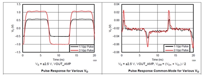
Figure 1: LMH5401 pulse response, differential (left) and common mode (right)
Now that we have reviewed the two main output modes of an FDA, let’s look at two potential alternative outputs: Out+ alone and Out- alone. For now, let’s use the identity of and look at what happens to the two primary responses with respect to one output only. For an FDA, the closed-loop gain = ) ; given the same loop gain using only one output, the closed-loop gain .This makes it clear that using only one amplifier output cuts the gain by 6dB, or by a factor of two. With an amplifier like the LMH5401, you can mitigate this drawback by using different external resistors to set the amplifier gain higher by a factor of two. Similarly, if you are using FDAs as attenuators, this gain reduction is an added benefit.
Using the same method, the amplifier common mode would change from to . This conversion shows that when using the single-ended method, the amplifier output common mode is no longer a meaningful concept since the common mode is simply equal to the output
To gain more insight into the amplifier performance, we’ll need to use more sensitive equipment than that used for Figure 1. With a spectrum analyzer, we can measure the amplifier distortion under single-tone conditions with a very high degree of precision. Figure 2 shows distortion measurements for the LMH5401.

Figure 2: Distortion measured with differential and single-ended outputs
Figure 2 clearly shows that the single-ended output does not provide the linearity of a differential condition. The output voltage for both conditions is 2Vpp. Note that in the single-ended output condition, one output running 2Vpp is the “same” as a 4Vpp condition for a differential output.
Given this serious handicap of single-ended operation, what happens when we drop the signal amplitude to make the conditions more comparable? Figure 3 shows what happens when you decrease the signal amplitude so that each output is swinging the same voltage, whether the results are measured in single ended or differential mode.
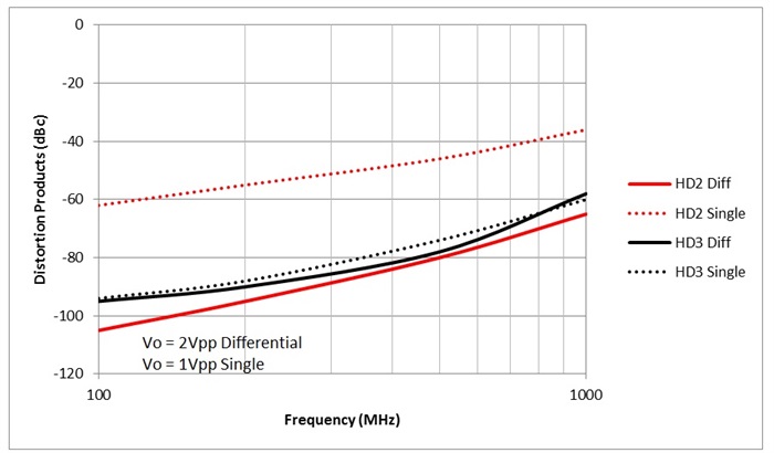
Figure 3: Distortion measured with differential and single-ended outputs
Figure 3 clearly shows that the third-order distortion products (HD3) are very similar for a single-ended output or a differential output – as long as you account for the amplitude penalty of single-ended outputs. The results for the second-order distortion products (HD2) are not comparable, however. This is the primary disadvantage of using an FDA with only a single output. While the HD2 of each output will cancel when the outputs are combined into a differential signal, this does not happen with a single-ended output.
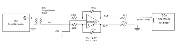
Figure 4: Test schematic
In conclusion, using a single output from an FDA may work in some limited applications: when the signal is at the lower end of the amplifier’s working frequency range, when the signal amplitudes are small, and when second-order distortion products are not a primary performance metric.
Related technical resources:
- Download the LMH5401 datasheet.
- Learn how to eliminate a power supply when using a fully differential amplifier (blog post)
- Learn how to use single-supply FDAs with negative input voltages to drive ADCs (technical article).
- Read about how to use FDAs as attenuators (technical article).
- Check out other high-speed amplifier blog posts.
↧
Simplifying higher current split-rail designs with Fly-Buck converters
Since 2011 TI has recommended using the Fly-Buck™ topology (or isolated buck topology) to simplify isolated bias designs for industrial and communication applications. The Fly-Buck design adds coupled windings to the inductor to provide single or isolated bias supplies without an opto-coupler. The LM5017 family is simple to use, reduces bill of materials (BOM) costs and increases performance, which is why it has gained popularity in the last few years.
Even though it’s popular, there is one constraint to existing Fly-Buck products – they are limited on total output power. The LM5017 is a 100V, 650 mA part, but in a typical 24V system, it can only support up to 5W output power before triggering the current-protection circuit. This limitation prevents the technology from expanding to more industrial applications. For example, a programmable logic controller (PLC) input/output (I/O) module requires 24VIN, isolated 24VOUT @ 500mA; in this case, the LM5017 could only support half of the required output power.
To meet these design challenges, TI has introduced the LM5160A, which expands the Fly-Buck portfolio and triples the power capability. The LM5160A not only easily solves the power-limitation problem; it also expands the technology to designers of broader applications like three-phase AC motor drives, power over Ethernet (POE) IP cameras and automotive.

Take the three-phase AC motor drive as an example to show how LM5160A simplifies the gate driver bias design. Figure 2 shows a typical AC motor drive system and bias supplies for the high- and low-side IGBT gate drivers. Positive and negative bias voltages are usually required due to IGBT characteristics.

The Wide Input Isolated IGBT Gate-Drive Fly-Buck Power Supply for Three-Phase Inverters reference design demonstrates the LM5160’s ability to generate eight isolated outputs from a 24V input bus. Three pairs of +15V and -8V are used to bias the high-side gate drivers, while the remaining pair (+15V and -8V) is capable of providing 300mA to bias all of the three-phase low-side gate drivers. The total output power is about 14W. Figure 3 shows the reference design board.

In addition to the AC motor drive, the LM5160A also addresses the higher bias power needed in PLC systems due to the increasing number of I/O channels. The Isolated Tri-output Fly-Buck Power Supply for Industrial PLC Applications reference design takes 24Vin and generates three isolated outputs: 5V@1A, +15V@200mA, -15V@200mA. All outputs remain +/-5% regulation over line and load regulation.
POE applications are booming these days, especially in the IP surveillance market. The LM5160A solution greatly increases power density and improves efficiency by more than 5% compared to traditional approaches. The Isolated Fly-Buck Power Module for POE Application reference design (PMP10572) demonstrates high density and high efficiency using a combined POE solution with the LM5160A and TPS2378.
These are just a few examples of the numerous options presented by TI’s expanded Fly-Buck capabilities. This approach will be successful in building automation; heating, ventilation and air conditioning (HVAC); elevator control; and automotive bias power in hybrid electric vehicles/electric vehicles (HEV/EV).
Additional Fly-Buck resources
- For more product information, see www.ti.com/product/LM5160A.
- For more Fly-Buck information and design resources, see the Fly-Buck landing page at www.ti.com/Fly-Buck.
↧
↧
“Driving” subsystem interconnect with voltage level translators

Automotive infotainment systems in the past have been predominantly based on a 5V and 3.3V voltage supply. This is due to a 12-14V battery that is readily available in automotive systems which can be stepped down to a lower voltage. However, there have been several key factors driving the need for lower voltage operation in infotainment, Advanced Driver Assistance Systems (ADAS) and cluster systems.

Over the past decade mobile and computing systems have made great strides in technology, which provide a flawless operation and a feature rich experience allowing access to multiple audio and video capabilities. Consumers are yearning for the same type of content and capabilities within their automotive infotainment system. What before was a single touch screen with Bluetooth, is now a multi-touch tablet size screen with web access, HDMI and USB interfaces.
Automotive tier-1 manufacturers are taking advantage of the electronics infrastructure that has been established for mobile and computing and repurposing it for automotive infotainment and cluster systems. These increasingly complex systems are modularized in a fashion where the OEMs can pick and choose features depending on the class of vehicle. To maximize the reuse of these mixed mode voltage systems requires the use of voltage level translators to connect these different subsystems.
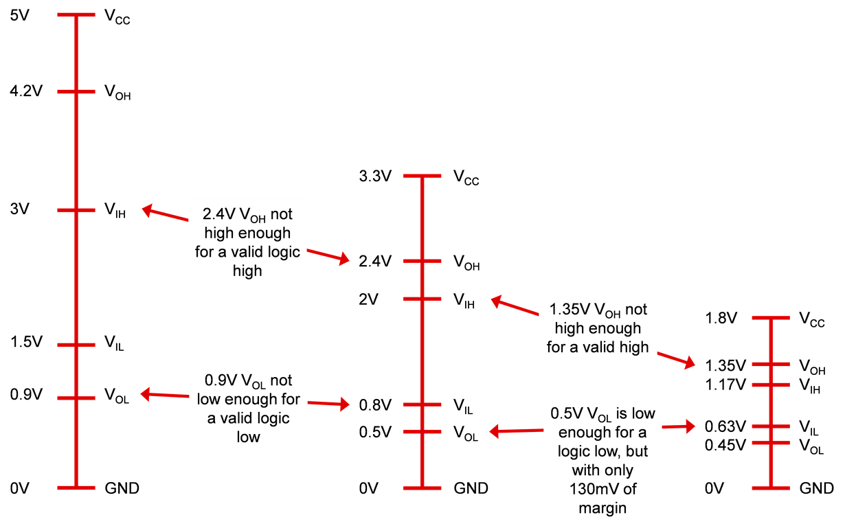
When interfacing 3.3V devices to legacy 5V systems, the problem is two-fold. The VOH of the 3.3V system cannot meet the required VIH threshold of the 5V system and the VOL of the 5V system cannot meet the VIL of the 3.3V system. The problem becomes hidden in even lower voltage systems where there are marginal VOH/VIH and VOL/VIL incompatibilities. A device may seem to initially communicate, but stop communicating because of the small margin between VOL and VIL. The threshold mismatches can manifest itself in these automotive extended temperature ranges.
To solve this issue, the engineer can use a full line of catalog automotive grade voltage level translators from Texas Instruments (TI). The SN74LVCxxT245-Q1, SN74AVCxxT245-Q1, TXB010x-Q1 and TXS010x-Q1 families are ideal for bridging this voltage mismatch where “x” indicates the number of bits or channels that need to be translated. Depending on the type of outputs (push, pull or open drain), loading condition, and direction of the signal, the appropriate solution can be used to “level shift” to the required voltages.
The SN74LVCxxT245-Q1 and SN74AVCxxT245-Q1 family is ideal for more heavily loaded buses where multiple devices are connected to the bus. These devices offer up to 12mA of current and is specified to drive up to a 15pF load. As such the main processor will need to control the flow of data of the device.
The TXB010x-Q1 series of devices are for those mixed voltage/mixed direction bus applications. This type of device requires no intervention from the main processor, making it a drop-in and forget solution. However, these devices are better suited for point-to-point bus applications given its relatively low current drive capability.
Much like the TXB010x-Q1 series, the TXS010x-Q1 does not require intervention from the processor, but is designed for open drain applications like I2C or for a reset/interrupt pin where there may be an external pull up voltage.
Next generation “start-stop” systems have battery voltages dropping below 3V. This is also accelerating the migration to lower voltage subsystems. Whether it is infotainment, cluster or ADAS, there will always be a need for voltage level translation.
To learn more about how TI drives Innovation, check out these other Automotive Innovation blog posts:
- Driving Innovation: In the right lane to making the drive safer, greener and more fun
- Eyes in the back of your head: Automotive radar goes mainstream
↧
Exploring the MSP430 tool chain: Part 5 – New MSP430 standalone GCC now available
This is the final entry of a five-part series to help you learn more about our robust MSP430 tool chain. Don’t miss Parts 1, 2, 3 and 4 on this blog from past weeks, because this week we focus on GCC for MSP.
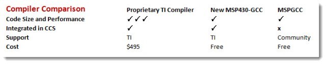
The new version (v3.02.02.00) of Red Hat’s GCC package for MSP430 MCUs has just arrived! It is the latest version of the successor of MSPGCC supporting all MSP430 devices without code size limitation. Being free and open-source, it includes GCC and GDB binaries for Windows and Linux, MSP430 header and linker files, source code and GBD agent configuration. You can get started with it both standalone and integrated with CCS6!

In addition to the features above, please check out what's new in this version!
- Large memory support in GCC (linker files update)
- Fixed loading of program into GDB with function in high memory
- Latest MSP430 device support (MSP430FR69x, MSP430FR68x, MSP430FR59x, MSP430FR58x, RF430FRL15xH)
- Several bug fixes (see release notes)
Can’t wait to get the new version GCC?
- Update your CCS v6.x installation (‘Help’, then click ‘Search for updates’) to the latest version and visit the CCS App Center under (‘Help’, then ‘Getting Started’)
- Use the standalone and open source downloads from the GCC tools folder
You can check out the basic migration advice and links to GCC documentation in the CCS v6 for MSP430 user’s guide.
Please provide any feedback on the MSP430 MCU E2E™ forum to help us continue making MSP430 development tools ecosystem better for you!
↧
Top trends in power innovation
Trends are often driven by some need that is not fully satisfied. This could range from fashion to entertainment to politics to even power management. Once a trend is recognized, opportunities for innovation kick off. Some trends have short lives, while others live for decades.
Trends in power have very long lives, perhaps because of the technical difficulties associated with new power-management technologies or the conservative nature of power-management industry. But just because a trend has been around, it doesn’t mean we should remain comfortable. A trend is no longer a trend when there are no more opportunities for innovation; however, a dormant trend can always be restarted when a technology enables new innovation. There are differences between trends and the technology that enables them.
Growing trends in power management include:
- Power efficiency.
- Power density.
- Energy harvesting.
- Digitally controlled power.
- Power-management tools for rapid design success.
- Wide VIN power.
- High integration.
- Smart power.
You will certainly find examples of innovations within these trends at the 2015 Applied Power Electronics Conference (APEC) in Charlotte, North Carolina.
Let’s focus on three of what I believe are the most significant trends where we will see the fastest innovation growth:
- Higher power density.
- Smart power.
- Energy harvesting.
Power density
Power density is almost like the “arms race” of the 1980s, with many companies spending their R&D dollars to take the lead. These companies are pulling out all the stops to process the most power in the least volume. Yet this trend brings many challenges, such as new topologies (bridgeless power factor correction), higher switching frequencies and of course improved power efficiency. In a supporting role, we have new technologies: wide-bandgap (WBG) devices such as gallium nitride (GaN) and silicon carbide (SiC) switching devices. We also need to support the ecosystem for this trend, which includes faster drivers and controllers that can manage the capabilities of the drivers and switching devices. Drivers with a sub-10ns minimum pulse width and even shorter propagation delays play a key role in enabling the technologies that support higher power-density trends. Many demonstrations of higher power density use high-performance digital-power controllers that do not consume much power themselves. These controllers need to have very fine edge control, as well as very fast data converters for loop control. Additionally, they also need circuits that can quickly calculate the response in time for the next switching cycle. So it is easy to see how significant improvements in power density are fertile grounds for innovation.
Smart power
Smart power is a major trend that addresses system efficiency by having the system manage the power subsystem. In the past, the power subsystem pretty much managed itself. Power designers could configure the supply for sequencing, soft start and stop, and fault-detection response based on the system requirements, but that was more of an initialization. Today’s systems demand much more real-time cooperation between the power subsystem and primary system. Industry interfaces like PMBus help with the standardization of interface and data protocols, but the real benefits come when the system and power supply cooperate. The system often knows in advance when it is going to change modes of activity that will require a change to power-system operation. Sharing this information with the power system allows the power supply to respond appropriately.
The big opportunities for innovation will come when the system and power subsystem can communicate at a much higher level. Today’s systems use dynamic voltage scaling (DVS), where the system tells the power subsystem to change the output voltage. Although this method is effective, so much more can be done. Communicating more information at a higher level can give more information to the multidimensional power supply, which better meets the needed response. Mixed-signal process technology provides designers opportunities for optimum partitioning. Power integrated circuit (IC) designers can closely couple the digital smarts with the optimum analog circuits. This allows integrated power converters to address the need for a smarter power subsystem to more easily cooperate with the main system. Future devices will accelerate this trend of addressing total system efficiency.
Energy harvesting
Energy-harvesting trends are key enablers to the Internet of Things (IoT). Many IoT devices rely on innovation in wireless connectivity, but to be really effective they need power that does not require wires. Batteries can certainly power the IoT, but then their replacement becomes an issue. Harvesting energy from the environment would be great as long as it provides all of the power needed. Harvesting environmental energy provides many opportunities for innovation. Improving the efficiency of the energy collector is an area under much investigation, but managing this energy is just as important. Environmental energy is not all that stable, so the energy must be stored in times of plenty for the times of little. In doing so, the energy-harvesting management unit should consume as little energy as possible.
Another aspect of IoT is that in order to minimize total energy needs, the peak-to-average power requirements are extreme; often more than 1,000 to 1. The energy-management unit needs to be able to handle these demands with very low latency while still consuming very little energy.
I would like to know your perspective on trends in power management, or the technologies that you think will start new trends or restart old trends. The list above includes my thoughts, and some of these trends will certainly have more activity than others. It doesn’t seem like it, but it was a decade ago that digital power control became a popular power-management trend and fueled many APEC conversations. It wasn't that it was a totally new trend, but it was restarted by innovations in process technology, where high-performance digital circuits could be integrated with high-performance analog circuits on the same die. We may see the same in areas where high-performance passives can be economically integrated in IC packaging.
It may be hard to tell if something is the chicken or the egg. Does technology start a trend or does a trend drive technology? I think it would be interesting to discuss this at APEC. One point is clear; we can no longer rely on long-lasting trends that patiently wait for innovation. Examples like Google’s Little Box Challenge show that if we don’t push innovation in our industry, others will.
TI at APEC
At APEC 2015, we plan to highlight several advancements in digital power and GaN technology and debut sophisticated new tools that help speed the design of power supplies for industrial, smart grid and automotive applications. Here are several demonstrations that will be on display in TI’s booth (No. 1001):
- Digital power: dynamic synchronous rectification control, end-to-end PMBus point-of-load DC/DC solutions, hardware and graphical software tools for digital power configuring and modeling, and tools for converting solar energy into electricity.
- DC/DC: wide VIN multirail power made simple with SIMPLE SWITCHER® nano modules and synchronous regulators, as well as automotive start-stop power.
- LED lighting: an efficient, step-down, high-power LED driver with strobe and synchronization for fire alarms.
- WEBENCH® power design tools and the TI Designs reference design library. TI will offer a USB stick to attendees with reference designs for many of the demos in the booth.
Some of our power experts will also present at technical sessions, including two focused on the impact of wide-bandgap power devices and how TI is making GaN technology more reliable.
For more information and to follow TI throughout APEC, see http://www.ti.com/apec15.
↧
Achieving Zero No-Load Power
Leading handset manufacturers recently set up a score chart rating system, in which stars are awarded based upon no-load power consumption, to encourage adapters to be designed for minimal standby power (Figure 1). Although there are demands for five star ratings, the ultimate goal is to drive the target rating down to a “zero-power” solution. An adapter is considered zero-power if its no-load power is measured to be less than 5mW when measured with an input voltage of 230Vac. Achieving less than 5mW of no-load power isn’t an easy task, as it involves compromises with other design targets.

Figure 1: Handset manufacturers developed a score chart to help consumers choose the most efficient handset charger based on no-load power consumption
Texas Instruments recently released a chipset: the UCC28730 zero-power primary-side regulation (PSR) flyback controller and wake-up monitoring and the UCC24650 200V wake-up monitor for fast transient PSR. This chipset provides a wide range of features that enable a <5mW standby power design without compromising design targets such as fast transient response, low component count and small size. Figure 2 shows a typical application of the UCC28730/UCC24650 chipset.

Figure 2: Typical flyback converter application using the UCC28730/UCC24650
A high-voltage startup switch eliminates the constant loss associated with a startup resistor. PSR reduces component count and the associated biasing losses for an opto-coupler and voltage regulator. The undervoltage lockout (UVLO) hysteresis of the UCC28730 allows the VDD voltage to drop as low as ~8V during standby without triggering UVLO. Using a low bias voltage of (for example) 12V at no-load combined with the low wait-state supply current (typically 52µA) will only “cost” approximately 0.624mW. The UCC24650 also has very low bias current (typically 41µA) and is biased directly from the output rail, resulting in approximately 0.205mW of power consumed in a 5V adapter. Total bias power uses less than 0.830mW of the total power-consumption budget.
Unavoidable losses that need to be accounted for would be the secondary-side leakage losses, associated with the output capacitor and the Schottky diode. A typical 10W design could result in leakage losses comparable to the bias power. The combined biasing power and these leakage losses constitute the minimum amount of energy needed to be delivered each switching cycle.
The act of delivering this energy creates losses proportional to the energy expended each switching cycle. The best overall way to reduce standby power is to reduce the switching frequency and to minimize the peak current during no-load conditions. The wide dynamic range of the UCC28730’s control law reduces the peak current to one-third its full-load value and allows the switching frequency to drop as low as 32 Hz at no-load, keeping dynamic switching losses low while sustaining standby operation.
With no-load power consumption minimized, the remaining design targets need to be considered. The low switching frequency would normally require large output capacitance to maintain output voltage regulation during large load transients. The UCC24650 is designed to send a wake-up signal to the UCC28730 so it can rapidly respond to load changes, minimizing output voltage droop without needing a large output capacitor.
The UCC28730/UCC24650 chipset can help achieve zero-power status by minimizing its own contribution to standby power, yet still operate in a way to minimize system-level losses. Together, the UCC28730 and UCC24650 require less than 1mW to remain active during standby, but are still ready to respond to sudden heavy load steps. The wide dynamic control range of the UCC28730 reduces the switching frequency and peak current during standby. With no external components required and minimal bias power, the UCC24650 wake-up monitor complements the primary-side UCC28730 to meet both no-load power and transient response. You still must pay strict attention to every possible contributor to ensure minimal collective standby losses, but achieving a five-star score or even zero power is achievable with the UCC28730 and UCC24650.
Here are a few reference designs using the chip-set that will help you on your way to Zero-power!
- 5V/10W off-line DCM flyback converter (PMP9561)
- 24V/12W off-line DCM flyback converter (PMP10927)
- Use this app note to deliver rapid transient response using the UCC24650 wake-up monitor with the UCC28633 high-power flyback controller.
↧
↧
Battery Terms Decoded: Part 1
Maybe you’re a firmware engineer assigned to write code to work with the battery charger and fuel gauge. Maybe you just want to know what your battery engineer friends are talking about during lunch. Whatever the case, you need a crash course in some battery terminology. Don’t worry, because there aren't too many terms you need to know, and it’s not all alphabet soup, either!
First, be sure to act clever and distinguish between the battery and the cell when necessary. The cell is just the bare Li-ion, Li-polymer or other electrochemical energy source without any protection, added electronics or packaging. A complete lithium pack, or battery typically has a small printed circuit board (PCB) attached to it with a protector integrated circuit (IC) controlling field-effect transistors (FETs) that will open in case of dangerous conditions like overvoltage or overcurrent. This protector IC is a minimum requirement for all lithium batteries due to the more “exciting” nature of this chemistry. There may also be a fuel gauge inside the pack, typically with a current-sense resistor; sometimes the protector and fuel gauge are integrated into one IC, as with the bq27742-G1.

Multicell packs may have even more electronics, like a chemical fuse, light-emitting diodes (LEDs) and cell-balancing circuits. And don’t forget the connector for interfacing with the battery. At minimum, the connector will have plus, minus and thermistor contacts. If it’s a “smart battery,” it will also have one or two connectors for communication with the gauge inside, perhaps a bq40z50.
Now let’s talk about shapes, or “form factors.” You can probably guess that a cylindrical cell is shaped like a candle. This is because it’s constructed like a jelly roll, with the cathode, separator and anode layers wound in a spiral before being enclosed in a metal can. Many thicker, older laptops have used multiple cylindrical cells in their battery packs for a long time. Cylindrical cells typically come in industry-standard sizes. The most famous is the 18650 cell, which has a diameter of 18mm and a length of 65mm.
The second type is also enclosed in metal for rigidity, but it’s usually a flat metal shape and is called a prismatic cell. Think of the increasingly rare flat removable batteries in mobile phones. Those are prismatic cells with a small protector PCB.
Now imagine that you want to get the thinnest possible battery to embed in your product. As long as users can’t remove the battery, you don’t have to encase the cell in metal, making a third type called a laminate cell or pouch cell an option. These names come from their construction, in which the cathode and anode layers are laminated to each other inside a flimsy foil pouch. This is typically the thinnest, flattest form factor you can get, but don’t puncture or bend it! These delicate laminate or pouch cells typically have the protector PCB connected to them by the pack maker; the entire assembly will be carefully embedded inside the final product, providing the physical protection. Users are not supposed to replace this type of battery themselves (at least not under warranty). Another good point is that custom laminate cells can easily be made with any dimensions, so you can fill exactly the volume allotted if your marketing department isn’t giving you infinite space.
I’ll close with a brief distinction between primary and secondary batteries. These are just fancy ways of saying non-rechargeable and rechargeable. If someone talks about their primary battery, they probably don’t mean their “main” battery. They mean a battery that is discharged once and disposed of. A primary cell can come in many shapes and sizes, but a common type is the “coin cell” like a watch battery. Traditionally they were non-rechargeable, but in recent years they, too, have been made available with rechargeable Li-ion chemistries.

With those basics behind us, in a future post we will get to that alphabet soup.
↧
A race against the clock: how to determine the power-up states of clocked devices
Many engineers choose flip-flops, shift registers, or other clocked devices for temporary storage and moving small amounts of data. These clocked devices have one or more clock-input pins, typically designated CLK or CP. A clock edge will determine when a specific function occurs; for example, the data may be clocked to an output, or data may be moved from one pin to another. Device data sheets specify whether this happens on the positive or negative edge, and include a truth table for each part.
Often, these truth tables include up and down arrows indicating the clock status. But what happens in that mysterious state before any clock edge has occurred? Consider the SN74AUP1G80, a five-pin D-type flip-flop. If VCC powers up and there is no valid clock edge, the truth table says that the Ǭ output is equal to Ǭ0.

Not very helpful, is it? Actually, it illustrates a design reality. We don’t know what the output will be before the first valid clock edge. When the device turns on, thresholds on internal transistors in the clocked device can float to indeterminate values, resulting in unpredictable signal levels at Ǭ. Typically, under the same conditions, the part will start up with the same output value, but this can vary across temperature and manufacturing lot to another. Therefore, for these clocked devices, it is imperative to wait until VCC has ramped to an appropriate level and a valid clock edge has passed before reading the output.
If the clock edge on a positive-edge-triggered device rises with VCC, I recommend waiting an extra clock cycle, as the clock threshold changes with VCC and any small amount of noise can cause unwanted clocking.
One clever trick you can use to “beat the clock” is to use devices with clear (CLR) (set all outputs to 0) and preset (PRE) (set all outputs to 1) inputs. Typically, in TI data sheets we designate these pins by some form of PRE, CLR or MR (for master reset). Look at the SN74AUP1G74, for example. The active-low CLR and PRE inputs allow engineers to override the clock! When used, these pins allow you to set the output of the device before CLK, giving you more control over the output bus.
For more advice on powering clocked devices, review these additional resources:
- Read this application note on how to select little logic or this app note on the power-up behavior of clocked devices.
- Search for solutions and share advice on the TI E2E Logic Community.
↧
Make sense of an uncommon reference
Often in high-power motor drives or industrial controllers, designers use closed-loop current sensors when their application requires a highly accurate representation of either AC or DC current. Also used in energy and hybrid electric vehicle (HEV) applications, a closed-loop current sensor can utilize a special sensor signal conditioning chip like the DRV411 that includes a Hall effect device as the feedback element.
In a recent user guide on a TI Design reference design (TIPD180), I explained how the circuit works when using a 5V supply and a fixed 2.5V reference. After publishing that design, I was asked, “How would the circuit work if the reference was fixed at 1.65V from an external source such as my analog-to-digital converter [ADC]?” Good question! Let’s work through the answer.
The drive stage of the DRV411, which provides current to the compensation coil, has a common-mode voltage that is fixed at VDD/2. When the supply rail is 5V, the drive-stage output has a common-mode level of 2.5V. The difference amplifier output stage of the DRV411, which provides the output voltage of the sensor module, uses the REFIN pin to set its common-mode output level. When the REFIN pin voltage is not equal to the internal VCM of the drive stage, current can flow through the series resistors in the difference amplifier, causing an offset error in the sensor module.

Figure 1: Uncommon VREF and VCM
Figure 1 provides an example where the DRV411 device is powered from a (max) 5.5V source; the reference is driven from an external ADC at 1.65V. The difference in voltage between the coil driver VCM and the reference is 2.75V – 1.65V = 1.10V. This voltage difference causes ~22µA of current to flow through the series resistors internal to the DRV411. Current also flows through the coil and shunt resistor, causing VOUT to be closer to 1.6513V.
When VOUT is fed into the external ADC for digitizing with its reference fixed at the original 1.6500V level, the primary current looks like it has a 1.34mV offset. Considering the 1,000 turns on the compensation coil, the 10Ω shunt resistor and the gain of four in the difference amplifier, 1.34mV of offset in VOUT is equal to about 33mA of primary current.

The TIPD180 was set up as a +/-50A sensor. Having a reference voltage lower than 2.5V will result in the sensor being able to go higher on the positive current measurements, but it will run out of headroom on the negative current measurements at around 40A.
Additional resources:
- Find out more in this app note, Design Considerations for the DRV411.
- Read more about the TIPD180, a single-supply closed-loop current transducer solution designed to accurately measure DC, AC and pulsed currents to +/-50A with galvanic isolation between the primary and secondary circuits.
- Get the most-used A/D conversion formulas in one handy guide.
↧