Rub the lamp and make a wish!
C.P. Ravikumar, Texas Instruments
The genie appeared when Aladdin rubbed the magic lamp. "Your wish is my command!" Integrated Circuits are like Aladdin's magic lamp. Rubbing this lamp with innovation can unleash the genie. Here is the story of an electronic lamp. It is the story of innovative product design from a University campus! |
I remember the winter morning on which I visited NSIT, Delhi. With help from Prof. Dhananjay Gadre, who is on the board of faculty of Electronics and Communication Engineering at NSIT, the TI India University Program was hosting four hands-on workshops in January. The event was technically co-sponsored by the IEEE Student Chapter of NSIT.
“Shall I make some coffee for you?” offered Gadre, and to my surprise, proceeded to make two cups of instant coffee using a microwave. In answer to my puzzled expression, he explained – “We keep the condiments for making tea and coffee in this office. My students use my office to do their projects. Some of them even sleep here if they have stayed up all night!” and pointed at the sofa.
I took a sip of hot coffee and looked around the office. Wires, soldering iron, printed circuit boards in various stages of construction, boxes, electronic components, text books. But there is a method in this madness, because Prof. Gadre is able to pull out what he is looking for without much searching.
I broached the subject of TI India Educators’ Conference, planned in April 2013. “Can you make an electronic lamp for the inaugural ceremony, Prof. Gadre?”
Like the coffee, his consent was also instant. I had seen his “birthday candles” project and wanted something similar, but being a free-lance designer, he likes to out-do his own prior designs.
“You may have seen the traditional brass lamp that is used in inaugural ceremonies. Perhaps you could build five small lamps that can be placed as five wicks for the lamp …”
“We will work on it,” he said, and smiled.
* * *
Here comes the lamp!
I told my team members about this conversation. Then we got busy with the preparations for the conference. At some stage, we received a list of semiconductors that Prof. Gadre needed for the lamp project and Vaibhav took care of that request. When we were about three weeks away from TIIEC, Prof. Gadre sent us a mail. The lamp project was going slow, but steady. He expects to have a prototype soon. We were prepared for the eventuality of using the conventional lamp as a backup.
The day before the conference, Sagar, Vaibhav, and I reached the venue at 5.30pm and got busy with some of the preparations we had to do. Prof. Gadre arrived at 8.00pm with a large suitcase. Very carefully, he took out the parts of the lamp and assembled them. He pulled out a matchbox from his pocket and an electronic matchstick. He rubbed the matchstick against the matchbox and the tip of the matchstick glowed milky white. He brought the matchstick in contact with one of the five lamps. The electronic wick caught on the light and began to flicker.
We were all smiles. “Hurrah!” we cried. “Bravo, Prof. Gadre!”
“But wait! The electronics works great. But we have this aesthetic lampstand that we have made for the lamp, which we need to assemble. That will take time.”
At this time, the electricity failed and we were covered with darkness. There was no backup power and we decided on the next action plan.
“There is no point in waiting here. Let’s go. I will be here by 6.00am and start assembling the lampstand. Your inauguration is at 9.00am. I will need at least 2 hours.”
* * *
The stage is all set
Apr 4. 8.45am. The “Silicon Hall” was beginning to fill up. The dignitaries who were going to “light” the lamp were already inside the hall, chatting, waiting for me (the host of the inaugural ceremony) to make an announcement. On the stage, Prof. Gadre and two of his students were kneeling on the floor, assembling the lampstand. Prof. Gadre had a soldering iron in his hand. He was pairing up wires of the same color coming from the power adapter and from the lamp and was going to solder them together. I looked at all this helplessly. What are the odds? I thought. Beads of perspiration formed on my forehead. Prof. Gadre’s steady hands continued to solder.
9.00am. The dignitaries in the front row occasionally looked up at the stage. The suitcase and plastic bubblewrap and boxes containing electronic components were still lying on the stage. Prof. Gadre was soldering. Should I act on the backup plan? The conventional lamp was ready, decorated with flowers and all. But the earnestness with which the students and Prof. Gadre were working did not permit me to say a word.
9.05am. I broke my silence. “Should we begin to clear the stage from the debris?” I said to one of the students. He obeyed. Just then, Prof. Gadre got up. The soldering was completed. Now for the acid test. He repeated the matchbox trick again – this time on all the five lamps. The first four wicks caught the light. The fourth one played hard to get. Wrong wiring? I thought. But Prof. Gadre held the matchstick for a little longer. The fifth wick obeyed. I rushed to the podium and began my welcome speech. It was 9.08am.
A successful lamp-lighting ceremony drew a thunderous applause from the audience. Then I invited our President and Managing Director Dr. Biswadip Mitra to say a few words, he chose to speak about the importance of building electronic systems. “My advice to students is to soil their hands. Choose a system, a sub-system, or even a sub-sub-system for implementation. Build it out of integrated circuits …”
I was thinking about Prof. Gadre kneeling on the floor, soldering the wires. “Surely his hands must be soiled,” I thought.
* * *
The lamp was made in many stages
Many days after the conclusion of the conference, I decided to ask Prof. Gadre to share the story of the lamp so that our readers from the Universities will be benefited. In particular, I am hoping that this story will help all those students who are starting out on projects using Texas Instruments integrated circuits.
“There were many stages during the development of the lamp,” said Prof. Gadre. The first stage was to form a team and brainstorm. A team of four worked with Prof. Gadre on this project – Rohit Gupta, Prateek, Piyush, and Rohit Dureja. More about the team later.
There are so many ways in which we could build an electronic lamp. We wanted a lamp that can be lit like a conventional lamp; simply pressing a switch will be breaking the tradition too much, although it will simplify things considerably. We also talked about several ways to trigger the lamp with the electronic matchstick. Finally, we settled on using infrared (IR) transmitter and receiver used in TV remotes. We tested out the idea by building a quick prototype – that was in the end of Jan.”
The second stage involved building the LED lamp with an integrated IR remote receiver. Several versions were built in February 2013. A final version was tested in early March 2013. The third stage was to build and test the electronic matchstick. This was done in March, about 3 weeks before the date of deployment. The matchstick uses an 8-pin MSP430, an infrared LED, a TPS61070 DC-DC boost converter and a 4.7F/2.7V super-capacitor.
After we got the lamp prototype to work, the next stage was decide on the structure of the lamp. “After much brainstorming, we decided to build a complete lampstand from acrylic sheets. Earlier, our idea was to build the lamp as an add-on attachment for the traditional brass lamp. In hind sight, building an entire lampstand was not a good idea – the stand was fragile and presented challenges in transport. It was also expensive to build.”
So there is a lesson in system design. Reuse what you can.
The final stage was to do “mass production.” Of course, in this case, the team only produced 10 lamps. This was done in the last week of March. “We clicked the image of the prototype, shot a small video demonstration, and sent them off to the TI team,” said Prof. Gadre. "A lot of care was taken to pack the lampstand and the lamps into a suitcase. I took an afternoon flight to Bangalore and when I checked in the luggage, I asked the airline to place a ‘Fragile’ label on my sturdy suitcase!”
* * *
Throwing some light on the lamp
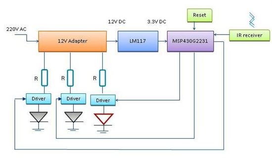
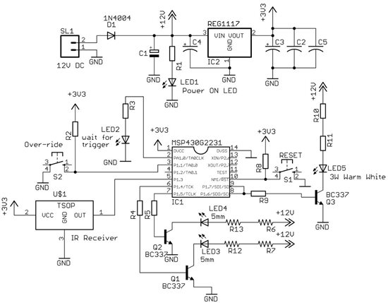
The lamp uses warm white High Brightness (HB) LED which is powered with 12V, as the main source of light. In addition, two lower power (100 mW) 5-mm warm white LEDs are used as additional sources of light to create a perception of flickering. The lamp is powered from a 220V AC mains supply; an adapter converts the AC voltage into 12V DC, which drives the LEDs. An LM117 Low Dropout (LDO) voltage regulator chip from Texas Instruments steps down the 12V DC supply to 3.3V required by the lamp controller circuit. The TV remote IC receiver is also powered with a 3.3V supply from the LM117 regulator. The lamp controller ccircuit also includes suitable drivers for the LEDs. To make debugging easier, the controller card includes a reset switch and an override switch, a power ON indicator LED and a status indicator LED.
![]()
Figure 1 - Block Diagram of the Lamp
A block diagram of the lamp controller appears on Figure 1. An MSP430 microcontroller has been used in the lamp controller circuit; in particular, a 14-pin DIP package was selected to simplify manufacturing. When the reset switch is pressed or when power is first applied to the lamp, a status indicator LED begins to blink, indicating that the controller is waiting for a trigger. The MSP430 microcontroller continuously waits for a trigger from the IR receiver or the press of the override switch. When either of these events happens, the microcontroller enters a loop where it shifts out bits from a 32-bit LFSR to the three output pins driving the three LEDs, creating a flickering light pattern. Providing the “override switch” allows the designer of the lamp controller card to independently test the card; it is also a valuable diagnosis tool for later use.
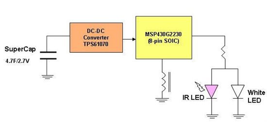
The electronic matchstick is powered by a 4.7F supercapacitor, charged to 2.5V using a pair of external AA batteries prior to use. The supercap drives a DC-DC converter that provides a DC supply voltage of 3.6V to an 8-pin (SOIC package) MSP430 microcontroller as illustrated in Figure 2.
![]()
Figure 2 – The Electronic Matchstick
The microcontroller in the matchstick drives two LEDs, a white LED and an IR LED. When the microcontroller is powered, it waits for a trigger signal from a 100mH sense coil. The trigger is provided by ‘rubbing’ the matchstick against conventional matchbox fitted with a couple of powerful neodymium magnets inside. When the matchstick is sharply struck against the matchbox (which side of the matchbox the matchstick is struck, is also important), a short pulse is induced across the sense coil and that triggers the microcontroller to light up the white LED using a random sequence of bits, thus creating an illusion of a real matchstick being lit. Also, the IR LED is fed with a sequence of ‘1’s and ‘0’s modulating a 40 kHz train of pulses. The 40 kHz carrier frequency is required because the IR receiver in the lamp has that requirement. The modulation of a carrier frequency with the required bit sequence offers immunity against unwanted ambient optical noise. The bit sequence transmitted by the IR LED is what triggers the LED lamp when the matchstick is held close to the lamp. The lamp waits for a sequence of five ‘1’s before lighting up. The white LED on the matchstick does not really have a role in lighting the LED lamp; it is only provided for creating an illusion of a burning matchstick!
* * *
The Team
Given that there were only three months to build the whole thing, four students were involved in the project. Rohit Gupta from Delhi Technological University helped in programming the MSP430 microcontrollers used in the lamp and the matchstick. “Piyush Guddu and Prateek Jha, alumni of NSIT, implemented the LED lamp based on a structural design I suggested. Piyush is an artist and Prateek transferred the design to Corel Draw, got the design fabricated, and raised the structure. He also did several designs of the lamp cover using the 3D printer we have in the TI Center of Excellence in Product Design. Rohit Dureja, a final-year undergraduate student of NSIT, helped in mass production. “Rohit Dureja is more experienced, can do better soldering and has some idea about testing,” says Prof. Gadre. “Since the volume was low, only 10 pieces, we managed everything in the lab itself, including the PCBs, soldering and testing.”
No project is without hiccups
To achieve the “flickering” effect, a random sequence of 0s and 1s are sent to a port pin that drives the LED. Rohit Gupta set out to program this on MSP430. Prof. Gadre told him about the Linear Feedback Shift Register (LFSR), which can be implemented easily on MSP430. The LFSR can generate a pseudorandom sequence of 0s and 1s. If these data bits are shifted at a suitable rate, the flickering effect is easy to create. Being an ambitious student, Rohit decided to try a different approach – use a pulse width modulation (PWM) generator to drive the LED. “This was an overkill,” said Prof. Gadre. “Moreover, there was something in the implementation which was causing the LED intensity to show a pattern in the short term.” In other words, the flickering was not random. Prof. Gadre sat down with Rohit for a debug session, when he realized that PWM has made inroads into the code. He advised Rohit to revert to the planned LFSR scheme, which, of course, worked! Once again, the lesson for the students is to “Keep things simple.” The lesson for mentors is to watch out for feature creeps in an ambitious student’s code!
There were other hiccups. “We noticed some minor errors in the lamp during its field trial,” says Prof. Gadre. “For example, we had not imagined that the flash light of the photographer’s camera could also trigger our lamp! Not sure how many people noticed this! Our plan is to correct this in the next version.”
System-level Design
Prof. Gadre had to think about other “system-level” issues as his students proceeded to carry out the design and implementation of the sub-systems. For example, he thought of adding a feature that can trigger the lamp without the matchstick. “There are two sub-systems – the lamp and the matchstick. Having an independent way to test the lamp will allow the design and debugging of the two sub-systems to proceed concurrently.”
Providing power supply to the lamp without adversely impacting the aesthetics was another concern. The lampstand was made of transparent acrylic material. Having a lot of wires running up the lampstand would be far from desirable. “We used copper tape for attacking this problem,” explained Prof. Gadre. “A vinyl cutter was used to cut the tape in required shapes and sizes. The copper tape was made part of the aesthetic feature!”
Transporting the lamp safely from New Delhi to Bangalore was no mean task. In the book “Soul of a new machine,” Tracy Kidder describes an incident that happened in a computer manufacturing company. The computer was assembled in a room on a higher floor. When the time came to transport the machine out of the office, the workers realized that the computer would not fit into the elevator!
“We were naturally worried about the acrylic sheets breaking. For transporting the fragile acrylic sheets, I had to think of a suitable scheme and I ended up using 6 mm plywood sheets of a size that would fit a large suitcase,” said Prof. Gadre. “I taped the acrylic cut sheets on these plywood sheets and then the entire structure could be transported safely. This has also been a lesson for us. Our next version will overcome these problems, so that the lamp has a higher acceptance in the market.”
Test, test, and test some more!
When the final prototype was ready, it worked just fine. The team then started the mass production, but continued to test the prototype lamp installed on the lampstand. One evening, when testing the lamp without the 3D printed covers, the lab assistant walked in and turned the tube light on. The team stared in disbelief – the lamp had been unintentionally triggered! The humble tube light has significant IR component and could trigger the lamp without the matchstick!
“There were only two days before the deadline. Fortunately, covering the lamp with the 3D printed covers protected the sensor from false triggering,” explained Prof. Gadre. “We heaved a sigh of relief. In hindsight, as we discovered during the conference, even this was not enough! The photographer was using a strong flashlight, which also has a very strong IR component, thereby triggering the lamps without the matchstick!”
The lesson here for students is to test the prototype as much as possible. Having it tested by someone who does not know the working principles of your project will also help!
I asked Prof. Gadre if their team has a solution to the false trigger problem. “The solution is simple – the matchstick and the lamp must trigger on a unique code of IR radiation and not just count 5 pulses of IR radiation, which happens in the prototype. Another lesson we learned at the conference was not to depend on AC power as the source of power for the lamps. Even during the conference, brief power outages happened and that turned the lamp off. In the new design, we are using batteries to power the lamps.”
What next?
I congratulated Prof. Gadre on the first product that officially rolled out from TI Center for Embedded Product Design at NSIT. To be precise, the lamp is the second product. “The Stellaris Guru” educational kit was the first product to be developed; but the Center had then not yet come into existence formally. I asked Prof. Gadre the questions that most people would be tempted to ask – will the design be available to someone who wishes to productize it? How does one approach the Center for this purpose? What support would Prof. Gadre and his team of students be willing to provide?
Prof. Gadre is willing to be a consultant for a company that wishes to bring out the electronic lamp as a product, either in its current form or with customized modifications. “The existing design as well as the new version that we are working on, will be made open source,” says Prof. Gadre. “If there is enough traction, we can think of making it available as a complete product or a DIY kit. I am available on e-mail to take questions about the productizing the lamp.”
Pictures!
Here is an attempt to capture the various stages of creation of the lamp!
![]()
Schematic Diagram of the Lamp | | |
![]()
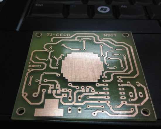
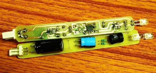
The bare PCB of the lamp controller | ![]()
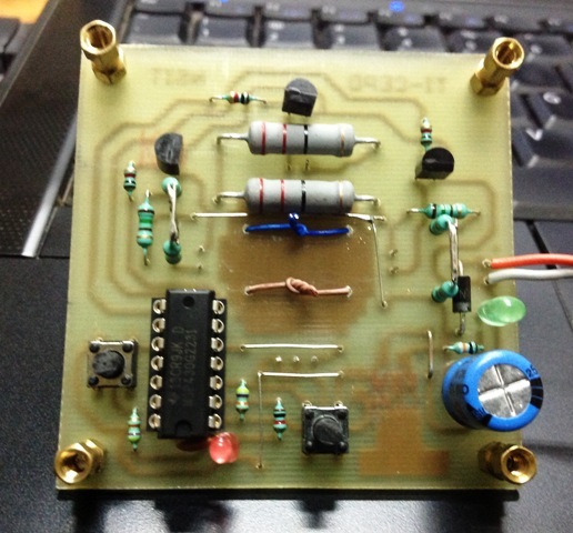
Top view of the lamp controller card | ![]()
Bottom view of the lamp controller card |
![]()
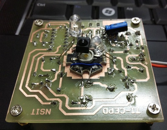
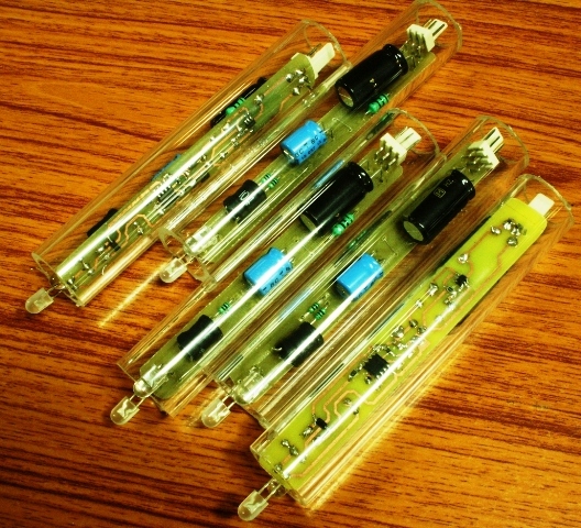
The assembled PCB of the matchstick | ![]()
Assembled Matchsticks | |
![]()
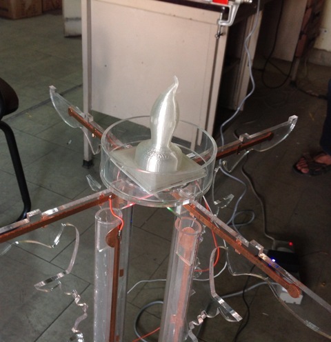
Lamp assembled on the stand. The lamp cover was printed by Prof. Gadre's team on a 3-D printer | ![]()
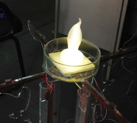
Picture of the glowing lamp taken at the stage of testing | |
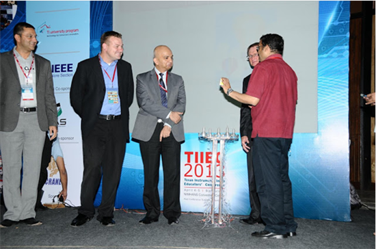
![]()
Prof. Gadre (in red shirt) explains the working of the lamp to the dignitaries who lit the inaugural lamp – Sanjay Bhan, Brad Ruzicka, Dr. Biswadip (Bobby) Mitra, and Steve Lyle are seen in the picture. | ![]()
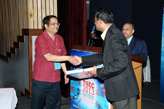
Prof. Gadre receives a memento at TIIEC 2013 from R. Madhu of Texas Instruments | |
![]()


 Equ. 1