Quantcast
Channel: TI E2E support forums
Viewing all 4543 articles
Browse latest View live

Wittra brings the Internet of “moving” Things powered by Sub-1 GHz and Bluetooth® low energy

$
0
0

Guest blog by Warwick Taws, chief technology officer, Wittra

Most of us can see the “Internet of Things (IoT) revolution” coming. It’s a fragmented landscape, with no dominant standard in any part of the technology chain. This can make it difficult to find where each of us fit into the overall ecosystem – how can we monetize our brilliant IoT idea? At Wittra, we see a differentiation opportunity in the “Internet of Moving Things”… being able to manage moving things (objects, people and animals) by knowing their position and activity.   To get a better understanding of our company and our products, we’ve answered a few questions below.

1.       What is Wittra?

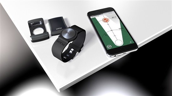
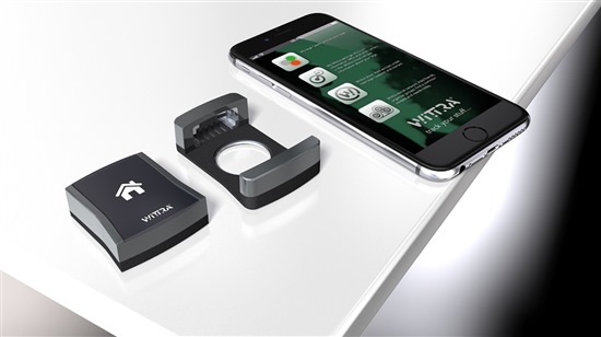
Wittra provides the world’s smallest, long-range mobile asset tag. This is paired with a fixed beacon (base station). Depending on your view of the world, we can be called an RFID, RTLS or IoT vendor. Our unique difference is our ability to perform distance ranging over our data link, at long range (kilometers), with low-power consumption. So we can triangulate the position of the tag if we have more than three available base stations, and operate both outdoors and indoors with a single product. We have a GPS chip in our tag, but we only use it if we can’t compute an accurate position from our network. In this way, we can offer months of battery life on a single charge.

Our customers are integrating this technology into products in diverse applications such as maritime safety for boat crews and passengers, pet lifestyle and activity monitoring, elderly care in the home (remote activity monitoring), vehicle security and tracking, race horse welfare and health monitoring, workflow management for trains in the shunting yard and workshops, shipping container tracking and management, warehouse/inventory logistics (pallet tracking indoors/outdoors), to name a few. We are seeing new applications every week and replacing existing technology solutions that have too many limitations to be effective.

2.       What makes Wittra stand out from its competitors?

We have recently won a number of positioning system deals where we beat the closest competitor on capital equipment cost by a factor of 10 – 20 times. This is a good example of what low cost, high performance silicon allows us to do. So cost is one area. Another is range – Wi-Fi® and Bluetooth® positioning systems measure distance in tens of meters (or perhaps a hundred meters)… we use kilometers as our baseline. GPS based asset trackers provide a few days of battery life – we measure battery endurance in months.

Our business customers are using this technology to provide their end users with new features and greatly improved product performance in many different market verticals.

3.       There are many wireless connectivity technologies on the market. Why did you choose to integrate Sub-1 GHz and Bluetooth low energy technology in Wittra?


Only Sub-1 GHz technology can provide us the unique advantage of long communication range and low power. You can’t ignore the laws of physics! Bluetooth low energy provides a complementary way to ensure seamless compatibility with millions of existing wireless devices already on the market, again using low power. Low power is the Holy Grail of small, battery operated end devices, because consumers don’t want the inconvenience of frequent battery charging.

4.      Why did you choose TI’s Sub-1 GHz and Bluetooth low energy connectivity technology for your product?


Of all the technology vendors, we saw that TI stood out in terms of RF performance, commitment to continued innovation, had a history of quality and consistency in delivery of functional silicon, and a willingness to support our product vision. We chose the SimpleLink™ Sub-1 GHz CC1310 and Bluetooth low energy CC2640 wireless MCUs to design into our product for those reasons.

5.       Where do you see your technology/solution going in the next five years?

In order to maintain our unique market advantages, we need to remain focused on innovation. We will make our end devices smaller, cheaper and more power efficient over time. This will enable us to enter more market verticals and provide our end users with a more compelling user experience and a better value proposition. Our fixed infrastructure beacons will become better at locating the end devices through more flexible radio architectures with more processing power and increased performance.

For more information, visit:


How to remove the ground-shift phenomenon from your capacitive-sensing application

$
0
0

There are many system requirements regarding sensitivity, responsiveness and power when using resonator-based capacitive sensing to achieve proximity detection. In end equipment such as automotive collision detection, white goods and personal electronics, grounded objects adjacent to the device can affect capacitive measurements. In this post, I will illustrate this phenomenon, referred to as a ground shift, under various grounding configurations.

Analytical model

Figure 1 models the ground-shift phenomenon through a simple circuit diagram of a resonator-based capacitive sensing solution and its parasitic capacitances where Cs is the combination of the board parasitics and the sensor capacitances, Cg is the parasitic capacitance between local and earth ground, and CP0 and CPg are the parasitic capacitances of a large local ground plane (if nearby).

Figure 1: Simplified circuit model with the resonator-based capacitive sensing device floating and a large local ground plane nearby

The oscillator signal alternates between INA and INB, so the circuit configuration is different for each half cycle of the oscillation. Since no other branch bridges the circuit with earth ground in either phase of the half-sine-wave excitation, Cs and (Cg + CPg) are effectively in series. This series relationship is given by Cx, characterized by Equation 1:

Therefore, the effective oscillation frequency is the average of the two phases, given by Equation 2:


Whenever (Cg + CPg) varies, β and Cx also changes, causing a shift in frequency and creating the ground-shift phenomenon.

System ground configurations either use earth ground or local ground. For example, if the capacitive-sensing device is connected to a battery-powered laptop and has no other connections to the external world, you may notice differences in performance than if both the laptop and the capacitive-sensing device are referenced to earth ground. In terms of the mathematical model, if the laptop is floating, Cg is negligible and if there is no nearby large local ground plane, then CP0 and CPg are negligible.

Qualitative assessment

To better understand this qualitatively, I ran an experiment using a laptop and TI’s FDC2214 evaluation module (EVM) with the standard sensors replaced by a custom bezel-shaped sensor. The sensor area is 55.8cm2 and I measured the proximity detections with a hand approaching within 10cm of the sensor. The white USB cable in Figure 2 connects the FDC2214 EVM directly to the laptop.

Figure 2 shows how the long black cable can also connect to earth ground or be left disconnected, leaving the system floating. A short black wire is soldered onto the copper side of the ground plane, allowing it to be either connected or disconnected from the FDC2214 EVM ground (Figure 3).

Figure 2: The setup consists of a laptop, USB cable, custom bezel sensor, FDC2214 EVM and large ground plane


Figure 3: The ground plane has copper on the backside (seen here) and FR-4 on the topside (seen in Figure 2)

Results

When the EVM is connected to a battery-powered laptop, the system ground is floating at an unknown value relative to earth ground. When a human hand contacts the laptop, the value of the AC ground may shift, causing an apparent shift in the sensor capacitance; see Figure 4.

Figure 4: Capacitance measurements of the system, with the laptop floating and no large local ground

An EVM connected to a nearby large local ground plane significantly reduces the ground-shift phenomenon, as the ground plane increases the value of (Cg + CPg) allowing β to be close to 1 and effectively shielding the sensor from any external ground coupling.

As expected from the circuit model shown in Figure 1, Figure 5 shows no significant response when touching the laptop. However, one thing to note is that the dynamic range of the proximity detection has decreased from 0.15pF to 0.04pF. Having a large nearby ground dilutes the signal and decreases sensitivity because of the introduction of a large ground-parasitic capacitance, CP0 (Equation 2). Even though sensitivity is reduced, the signal quality is still decent – around 11dB.

Figure 5: Capacitance measurements of the system with the laptop floating, but also with a large local ground connected to the EVM

Summary

The ground-shift issue resides in the fact that the sensor capacitance is in series with the parasitic capacitance between local and earth ground. One of the ways to mitigate this issue is by connecting the capacitive-sensing device to a large local ground plane. This effectively allows for shielding from external ground-coupling noises.

I’d like to know if you try this technique or if you have another technique for removing ground shift in your capacitive sensing design. Log in to post a comment below!

Additional resources

Out of Office: Carving serenity from stone

$
0
0

HeaderYou could say TIer Ethan Davis’ life strikes a good balance of leading edge and age-old.

His work centers on the high-tech, ever-advancing world of developing products for automotive and industrial applications.

His home life takes on a much more zen-like state as he practices the age-old art of stone carving.

Think Michelangelo.

“I like the permanence of stone, the feeling it’s something that can last,” he said.

carvingEthan took a rock carving class about five years ago at the Dallas Creative Arts Center and was instantly hooked. He had always wondered how people made the ancient architecture he saw while living and working as a TIer in France and Japan.     

His hobbies, which include gardening in addition to stone carving, help him manage the everyday stress of working on complex programs. A TIer for 26 years, he currently manages the program management team in our Processors business unit.

Typically carving marble and limestone, Ethan prefers architectural stonework – making items that are functional as well as beautiful.

Many of his sculptures, such as a 35-foot arched gateway, adorn the large garden at his Dallas home.

“I would love to see him in action,” said Mike Wagner, a program manager in our battery management unit who has known Ethan for years. “The finished products are quite impressive.”

GardenWagner and other TIers have seen some of Ethan’s sculptures during happy hour and dinners Ethan occasionally hosts at his home.

The challenge of stone carving is that “you only get one chance,” Ethan said. “If you break it, it’s gone and you have to restart.” Yet he loves turning a block of stone into a work of art.

“With stone the art is waiting inside, you can create something fantastic,” he said. “Like with work, you have to have a vision and make a plan.”

Ethan started carving small items, such as a 14-inch lotus flower, but they kept getting bigger and bigger.

His largest, longest and most difficult project so far was turning what started as a 1,800-pound piece of limestone into a copy of a section of the west Parthenon Frieze – the giant stone relief of horses from around 440 BC that’s part of the Elgin Marbles at the British Museum in London. It took nine months to carve and about three months to install the three-and-a-half-foot by five-and-a-half-foot frieze on Ethan’s garden patio wall.

gardenEthan picked up his interest in gardening from his grandmother, whom he remembers helping with her roses as a teenager in his native Kentucky.

“These kind of hobbies make you more self reflective and, in a way, more balanced and ready to take on the challenges of the crazy work we’re doing,” Ethan said.

Taking his pursuit of balance even further, Ethan began practicing yoga and meditation in the last year.

Coworker Sapna Setty, a software program manager in Embedded Processing who introduced Ethan to meditation, said she can see its effects in him.

“Once you manage inner wellbeing, it shows big time at the way you come to work and handle the work,” Sapna said. “I have always known him to be very calm in any situation, including emergency situations.”

How to leverage the flexibility of an integrated ADC in an MCU for your design to outshine your competitor – part 1

$
0
0

Have you wondered why MSP microcontrollers (MCU) offer flexibility in its integrated analog-to-digital converters (ADCs) such as programmable resolution or power modes? This degree of flexibility is typically not offered in standalone ADCs. Developers can use MSP MCUs for multiple applications to leverage flexibility to optimize performance, ease of use and power consumption for a variety of applications. Recently, we explored increasing ADC performance by oversampling the 14-bit ADC integrated into the MSP432™ MCU on Analog Wire.

Today, I will focus on a few key performance features of the MSP432P401R MCU’s 14-bit ADC, named ADC14, which offers the flexibility to customize for your application:

  • Performance features:
    • Reference options
    • Select single ended or differential input per channel
    • Programmable number of bits

Reference options

Selectable reference options for the ADC14 allows for flexibility to have the best reference voltage for different applications. The reference voltage must be larger than the maximum input signal but the closer to the maximum input signal value the better resolution the ADC will have because the step size will be smaller. The internal reference can be chosen with ADC14VRSEL bits and the voltage selected as 1.2V, 1.45V, or 2.5V with REFVSEL bits. The internal reference can even be outputted externally (with REFOUT bit) to power the sensor for ratiometric measurements or vice versa by using the AVCC supply to source the ADC reference voltage and the sensor. If the internal reference and AVCC supply don’t offer the required voltage, then pins for an external reference voltage can be selected.

Here is an example showing the increased resolution by selecting the optimal reference voltage. Input signal is 1V and 14-bit mode is selected for this example:

With a 2.5V reference it results in a 14-bit ADC resolution of 153uV per code

With a 1.2V reference it results in a 14-bit ADC resolution of 73uV per code

In this case using a 1.2V reference with a 14-bit ADC provides better resolution than a 15-bit ADC with a 2.5V reference. Thus, a lot can be gained from choosing a lower reference voltage greater than the maximum input signal.

Single-ended or differential input

Single-ended or differential input can be selected per conversion with the memory control registers ADC14MCTLx. This allows true differential mode support, i.e., 0 - VREF common-mode when needed to simplify on-board signal conditioning circuit, thus reducing cost and system power. The ability to select differential input for one required input channel and single-ended for the rest maximizes the pins usage of the device as differential input requires two input pins vs the single-ended only requires one pin.

Programmable number of bits

The ADC14 offers a programmable number of bits 8, 10, 12, or 14 with ADC14RES bits. There is less clock cycles required to complete a conversion as you reduce the number of bits, so select the minimum number of bits required to both maximize sample rate as well as minimize energy. This allows applications which prioritize speed such as fault detection to select a lower number of bits and applications where speed is not critical, such as temperature measurements, to prioritize resolution. As the number of bits is programmable, it can even be changed between conversions based on requirements of different parts of the application code that may require different ADC resolutions.

To get started, order our easy-to-use MSP432 MCU LaunchPad™ development kit.

If leveraging the 14-bit ADCs flexibility to leverage ease of use for your application is interesting – stay tuned for the next blog in this series where I will discuss ease of use features for ADC14 on MSP432 MCU.

For those of you developing on an MSP430™ microcontroller, the "ADC12B" inside the MSP430FR5x/MSP430FR6x MCUs have similar features. 

Additional resources

eFuses: clamping and cutoff and auto retry, oh my! – part 1/3

$
0
0

Much like when Dorothy arrived in Oz, your first look at the multitude of features inside the Texas Instruments eFuse portfolio can be overwhelming. With options such as voltage clamping, circuit breaking and auto retry (to name a few), our portfolio can help protect almost every power circuit.

But with so many choices, picking the perfect eFuse can pose a challenge. The goal of this three-part blog series is to simplify your eFuse selection process by removing the confusion surrounding the options for overvoltage (part 1), overcurrent (part 2) and fault response (part 3).

We’re off to see the wizard down the yellow brick road of circuit design.

As you begin your journey down the Yellow Brick Road, you come to the first fork: overvoltage protection (OVP). Figure 1 shows two options: output-voltage clamping and output-voltage cutoff. Before deciding which path to go down, let’s take a look at the benefits of each, starting with the simpler and more common of the two options: output-voltage cutoff.

The benefits of output-voltage cutoff

An eFuse with output-voltage cutoff will generally have an OVP pin where an external resistor can set the trip point. As an example, let’s set the trip point to 15V. During normal operation, a 12V rail will not trip the comparator, and the internal FETs will remain closed; the device will stay on. However, a transient of 18V will exceed the trip point and the internal FETs will open, turning the device off. Figure 1 shows this operation.

Figure 1: eFuse output-voltage cutoff example using the TPS25940

Once the input voltage (VIN) exceeds 15V, the eFuse turns off and the output voltage (VOUT) falls to 0V, as shown in Figure 1. The eFuse will remain off as long as the input voltage exceeds the set overvoltage trip point. Once the input voltage returns to 12V, the device turns back on and VOUT once again returns to 12V. Because output-voltage cutoff disables the eFuse when active, it will never trigger a thermal shutdown.

While this is the most common form of overvoltage protection in the Texas Instruments eFuse portfolio, it may not always be the best. Sometimes it is beneficial to keep a voltage rail alive for as long as possible by clamping the output voltage to the nominal voltage.

The benefits of output-voltage clamping

Contrary to output-voltage cutoff, during output-voltage clamping the eFuse remains operational. When the input voltage exceeds the hard-coded trip point, the internal clamp will activate and limit the output voltage. As shown in Figure 2, the TPS25924 eFuse integrates a 15V output clamp.

Figure 2: eFuse output-voltage clamping using the TPS25924

You can see in Figure 2 that when the input voltage spikes from 12V up to 18V, the clamping circuitry activates and ensures that the eFuse only outputs 15.6V (typically 15V). If the transient on the input is only temporary, this can allow the eFuse to “hide” the fault from downstream circuitry. If the fault lasts long enough to activate the eFuse’s thermal shutdown (typically TJ = 150°C), then the fault will still cause the eFuse to turn off (similar to output-voltage cutoff). After thermal shutdown, all eFuses then enter one of two fault-response modes: either latch off or auto retry, both of which I will cover in the third part of this series.

But first, stay tuned for part 2, which will delve into overcurrent event-response options: current limiting and circuit breaking.

Additional resources

Inductive sensing: Switch applications made simple

$
0
0

Switching and latching applications that involve detecting the presence of a moving object can be complicated to design and plagued by reliability problems. Examples include implementing tamper detection for opening and closing doors, or measuring the rotational speed of a gear regularly exposed to dust or oil that could block the sensor and cause failures.

Additional challenges exist depending on the specific technology used for the switching application, including:

  • An inaccurate switching threshold due to the requirement of an additional component such as a magnet or magnetized material, which is often not very accurate due to variations between parts and often requires calibration in production.
  • Temperature variation and component aging, which affects the accuracy and repeatability of the switching threshold.

The introduction of TI’s LDC0851 differential inductive switch enables a new approach that offers a temperature-stable switching threshold accurate to 1% of the coil diameter, eliminating the need for production calibration.

LDC0851 differential inductive switching theory

The LDC0851, as shown in Figure 1, uses inductive sensing to perform a simple inductance comparison between two matched printed circuit board (PCB) coils. The output switches high or low depending on which coil has less inductance.

Figure 1: LDC0851 differential inductive switch functional diagram

Application examples

This new approach to switching applications offers benefits for two main categories of applications:

  • Proximity-detection applications that need a contactless and repeatable switching threshold, such as simple buttons, door open/close detection mechanisms and industrial proximity switches. Figure 2 shows a proximity-detection application in which an LDC0851 senses the position of a snap-dome button without electrical contact. Figure 3 shows that the adjustable threshold allows for easy prototyping and fine-tuning the response to detect the button response.

Figure 2: Proximity detection for an example button application

Figure 3: Adjustable threshold to fine tune button response


  • Event-counting applications that need to work well in dirty and harsh environments, such as flow meters, gear speed measurement devices and rotary encoders benefit from robust nature of inductive switching. The TI Designs Inductive Sensing 32-Position Encoder Knob Reference Design Using the LDC0851 shown in Figure 4 implements a 32-position encoder knob commonly found in automotive infotainment or appliance interfaces such as cooktops and volume knobs.

Figure 4: LDC0851-based encoder-knob reference design

Prototyping tools and resources

A simple coin-cell battery-powered evaluation module (EVM), shown in Figure 5, demonstrates close-range proximity sensing as well as simple on/off metal-button detection. This EVM includes a perforation that enables you to replace the default sensor with a custom sensor.

If you’re interested in learning more about the new inductive switch, the WEBENCH® coil design tool can help simplify the design of stacked coils for the LDC0851. In the next post, we will go through a design example and show you how to use the new tool.

Additional resources

Is water flow metering important in today’s economy?

$
0
0

Can you imagine a cab without fare meters? Without a fare meter, the cost to drive around the block or travel between two cities would cost the same. Similarly, it is difficult to charge for water services fairly without a water meter. Thus, meters of all kinds have become integral parts of our economy and lifestyle – in scientific testing, machine alerts and maintenance, resource conservation, and the way utilities bill for services.

What is a water flow meter, and why do utility providers install them?

A water flow meter is a type of measurement instrument fitted onto a pipe through which water flows. The meter continuously monitors the water flowing through the pipe to calculate the volume of water flow.

Utility providers that supply water to commercial and residential properties install water meters in order to charge customers for this valuable natural resource and to manage water consumption effectively. Some people regard meters as the fairest way to charge for water services.

There are other ways to use water meters:

  • To determine the existence of a leak – if a meter continues to record data even with the water turned off, there’s a leak somewhere.
  • To measure water produced by a well.
  • To distinguish water usage among tenants in a multitenant building.
  • To separate water used inside buildings from water used for landscaping. Dedicated irrigation meters make it easy to monitor irrigation water and ensure that utility providers are only charging sewage for water used inside, not outside.

Benefits of water meters

Installing water meters benefits not only utility providers but consumers. A water meter’s benefits to utility providers include the ability to:

  • Measure the amount of water their customers use.
  • Generate monthly bills based on the data that meters collect.
  • Detect leaks and waterline breaks in the distribution system.
  • Monitor their water supply (making sure they have enough to supply everyone).
  • Safeguard water services for the future and provide the best value for customers.

A water meter’s benefits to consumers include:

  • Reduced operating expenses through lower bills.
  • Potential increase in property values.
  • Having residents pay for their specific water usage even if they live in a multitenant property, where separate meters are used to sub-meter separate units within a homeowners’ association or apartment building.
  • Contributing toward resource conservation by managing water usage efficiently.

To better understand how to achieve these benefits, it’s important to first understand water flow measurement and how meters are read. Stay tuned for the next installment in this series to find out.

Get started on your water metering design:

For more details on our system solutions for the global smart energy grid, be sure to check out ti.com/smartgrid and ti.com/flow.

Meet Mongoose, your new IoT middleware

$
0
0

This blog was authored by Deomid Ryabkov, Software Engineer, Cesanta

Mongoose is one of the most widely used embedded web servers and multi-protocol networking libraries available. Engineers use it as an Internet of Things (IoT) middleware, solving various tasks from internal servers to creating customer facing dashboards.

Mongoose integrates seamlessly with TI’s SimpleLink™ Wi-Fi® CC3200 wireless microcontroller (MCU) andMSP432™ MCUs. It runs on SimpleLink Wi-Fi’s on-chip user dedicated MCU, and utilizes its embedded HTTP server and built in TCP\IP stack, in order to provide a high-level interface for protocols like TCP, UDP, HTTP, WebSocket, MQTT, CoAP and DNS - for both client and server side. 

A deeper dive into Mongoose

Mongoose is both a server and client networking library. It is available on multiple platforms and offers a common programming model. For example, you can write client/device code and cloud/server code using the same programming model.

Mongoose uses a unique approach to the SimpleLink Wi-Fi built-in HTTP server. You can create a connection manager object and then one or more connections. Each connection has an associated handler function which is invoked for all events associated with it. The connection can be a server listener or an outgoing client connection, with or without a protocol handler (such as HTTP or MQTT) attached to it.

The handler function’s signature is the same for all event types:

void ev_handler(struct mg_connection *nc, int ev, void *ev_data)

The particular set of events (ev) received by the connection will differ depending on which protocol is used.

The best way to learn is to read the documentation or browse through some examples.

Working Examples

Let’s take a look atSimpleLink Wi-Fi CC3200 wireless MCU examples (everything described below also applies to the MSP432 MCU with a SimpleLink Wi-Fi CC3100 wireless network processor BoosterPack™ plug-in module).

You will need:

  1. CC3200-LAUNCHXL dev board
  2. CC3200SDK1.2.0 installed in TI_PRODUCTS_DIR/CC3200SDK_1.2.0 (typically C:\ti\CC3200SDK_1.2.0 on Windows)
    1. The accompanying CC3200SDK-SERVICEPACK should also be installed and flashed to the device
  3. Code Composer Studio 6 IDE
  4. Mongoose source code. Either clone theGit repo or download theZIP archive.

Mongoose - The library project

The Mongoose project produces Mongoose.lib - a static library meant to be used by other projects, such as the demo projects below.

Feel free to use it as a dependency for your own projects or just copy mongoose.c and mongoose.h. Note that by default a lot of features are enabled, including file serving (which we use in our examples). You can trim a lot of fat by turning variousbuild options off. A minimal HTTP server configuration is about 25 K (compiled for ARM® Cortex®M4 with GCC 4.9 with size optimization on).

MG_hello - A simple demo

MG_hello project is a simple web server that serves files from the SimpleLink file system and allows them to be uploaded. This project depends on the Mongoose library project. Make sure you import them both. When importing, ensure the “copy project to workspace” checkbox is unchecked, otherwise file references will be broken.

When built and run on the device, by default, the example will set up a Wi-Fi network called “Mongoose” (no password).

Assuming everything works[1], you should see the following output in CIO:

main                 Hello, world!

mg_init              MG task running

mg_init              Starting NWP...

mg_init              NWP started

wifi_setup_ap        WiFi: AP Mongoose configured

Note: If the demo does not proceed past “Starting NWP…”, please reset the board (possibly related tothis and ourworkaround is not always effective).

And, after connecting to Wi-Fi network Mongoose, the following page onhttp://192.168.4.1/ :


Pick a small file (at most64K; sayfavicon.ico) and upload. You should get “Ok, favicon.ico - 16958 bytes.” and it will be served back to you (link). If you upload index.html, it will be served instead of the form (but the form will be accessible at/upload)

Now let’s look at how it works under the hood. Mongoose is event-driven. User code is executed in event handler function, which receives an event and can either react to it or ignore. Roughly, the plan is as follows:

  1. Create and install a connection manager
  2. Add a listener
  3. Invoke mg_poll periodically to process events.
  4. Handle incoming connections in the event handler.

An even simpler, non-TI-specific example calledsimplest_web_server illustrates this.

The ev_handler function is where all the action is. It receives event, one of them being MG_EV_HTTP_REQUEST, which it then passes on to a built-in mg_serve_http function, which serves files from the file system. Other events - MG_EV_ACCEPT, MG_EV_CLOSE - are ignored.

Let’s go back to our SimpleLink Wi-Fi CC3200 wireless MCU example. Here we take a slightly different approach. First, we don’t want to block main thread and instead spawn a separate task which will do the mg_polling business for us (line 216). You can find the definition of mg_start_task in mongoose.c. It’s a pretty straightforward utility function which creates a queue and a task.

Mongoose is single-threaded. Internally, it does not perform any kind of synchronization. You as the user must ensure that everything that touches the state (the mg_connection struct) happens in a thread-safe manner. The easiest way, without introducing mutexes, is to either do everything in the event handler function itself or in a callback invoked from the same task. For this purpose, mg_run_in_task function is provided. It takes a callback pointer as well as a data pointer and will execute it on next iteration.

Theevent handler function in our example is somewhat more elaborate. More events are handled and for http requests we check the URL and existence of index.html and either serve the static file upload form or fall through to file serving. We also handle events related to streaming file uploads, which we ultimately just forward to the built infile upload handler to serve /upload.

MG_sensor_demo - A more elaborate demo project

This demo shows the use of timers and serving a WebSocket data stream to multiple subscribers. Data from the on-board temperature sensors and accelerometer is streamed to any clients connected over WebSocket, which allows building of responsive, near-real time dashboards.

MG_sensor_demo’sevent handler function in main.c does everything MG_hello’s function does, but also handles the websocket connection event - when MG_EV_WEBSOCKET_HANDSHAKE_DONE arrives, it switches the event handler to a different one - data_conn_handler (definedhere in data.c). Doing this is not required, but it keeps the code modular and function size manageable.

Data acquisition is performed at regular intervals by a timer. Mongoose’s timers work well for this case. Remember, everything is executed in single thread.The timer is first setin mg_init(), and the MG_EV_TIMER event is handledin the main handler. Mongoose timers must be re-armed manually.

To try this demo from Code Composer Studio™ integrated development environment (IDE), follow the steps above for MG_hello. As for MG_hello, you will only see an upload for initially. Please upload main.js and index.html from theslfs folder and reload the page. You should see something like this:

This short video shows the demo in action.

Try it for yourself

Feel free to check out the code yourself, especially the WebSocket data connection handler. 

You can download Mongoosehere

The good news are that as long as you are testing and prototyping, the use of Mongoose is free under GPLv2 licensing. For commercial use you have a choice between acquiring a license or open source your solution. . We’d be happy to discuss this with you, feel free to contact us.

But for now, feel free to dive in and experiment today!

Additional resources:


[1] If the network does not appear or you cannot connect to it, please use existing Wi-Fi network - enter the SSID and password at the beginning of main.c.


Keeping up with the standards: Efficiency and standby power requirements

$
0
0

Energy agencies around the world are concerned about growing power consumption and the amount of available deliverable energy. One of the largest demands on the world’s power grid comes from external power supplies (EPSs); these include laptop adapters and phone and tablet USB chargers/adapters. Portable electronics users probably use two to three EPSs every day.

To help conserve energy and reduce waste, these agencies created initiatives and legislation to compel power-supply designers to develop offline power supplies with higher efficiency and lower standby power. The most popular standards for EPSs are the European Code of Conduct (CoC) EPS V5 Tier 2 energy-efficiency standard and the U.S. Department of Energy (DoE) EPS Level VI efficiency standard. The CoC standard is voluntary; however, a majority of power-supply manufacturers in the European Union (EU) are ensuring that their designs meet its requirements anyway. The DoE efficiency standard is mandatory.

Both standards segregate their requirements into power and voltage ranges. In this post, I’ll focus on the low-voltage (<6V) and lower power (<250W) efficiency and standby power requirements.

Tables 1 and 2 list the CoC and DoE standby power requirements for low-voltage/low-power EPSs. You can see that the EU’s voluntary specifications are slightly stricter than the DoE’s mandatory specifications. Designers generally use flyback converters as offline power converters in this power range. The more traditional fixed-frequency pulse-width-modulated (PWM) controllers with higher integrated circuit (IC) standby current would have difficulty meeting either specification. The power dissipation caused by the trickle-charge bootstrap resistor when starting up these older PWM controllers alone could cause the design to fail the standby power requirements.

Table 1: CoC Tier 2 EPS Low Voltage, Standby Power Requirements

Table 2: DoE Level VI EPS Low Voltage, Standby Power Requirements

To meet these needs PWM manufacturers like Texas Instruments have developed ICs with lower standby current, which enable the use of higher-impedance trickle-charge resistors to reduce standby power (the UCC28704). They have also developed green startup circuitry internal to the PWM controller (the UCC28730) that only dissipates power on initial power up, also reducing standby power.

Plus, primary-side regulated controllers, such as the UCC28704 and UCC28730, regulate the output through the primary to secondary transformer turns ratio and do not require opto-isolator feedback, reducing standby power even further.

In the past, designers would focus on the maximum load efficiency and not spend much time evaluating overall efficiency. This is mostly because of the power-dissipation and power-density requirements. To help increase EPS overall efficiency, the CoC has specifications for four-point efficiency and 10% load efficiency (Table 3). The average efficiency is based on the average of the efficiencies of the power supply taken at 25, 50, 75 and 100% loads. As I mentioned earlier, the DoE average efficiency standard (Table 4) is not as stringent as the CoC standard, and does not include a 10% load efficiency requirement. The DoE standard does calculate average efficiency at the same load points as the DoE.Please note In Tables 1 through 4, the variable Pno stands for the power supply’s nameplate output power. A traditional fixed-frequency flyback converter would have difficulty meeting these efficiency standards, mostly due to switching losses.


Table 3: CoC Tier 2 EPS Low Voltage Average and 10% Efficiency Specifications


Table 4: DoE EPS Low Voltage Average efficiency Specifications

To help meet efficiency requirements in the 1W-25W range, flyback controllers have been designed with FM/AM/FM modulation schemes These controllers modulate the converter’s switching frequency (FM) and primary peak current (AM) in order to control the offline converter’s duty cycle, reducing the power converter’s average switching and conduction losses. To help improve efficiency even further, these controllers use valley switching to reduce switching losses.

In the 25W-250W range, designers generally use quasi-resonant flyback controllers. These controllers are inherently soft switching, with reduced switching losses. Some of these controllers will have burst-mode operation and power-management capability to improve overall efficiency and reduce standby power. One example of power management is to turn off the power factor correction (PFC) pre-regulator at light loading, a feature that some flyback controllers have. PFC is not required below 75W, and turning it off will improve system efficiency below 75W and reduce standby power.

As the world consumes more and more power, being compliant with the EPS V5 Tier 2 and the U.S. (DoE) EPS Level VI efficiency standards becomes imperative. PWM controllers with lower standby current can help reduce stand by power.

Be sure you’re meeting the standards and learn more about TI’s PWM controllers. 

The rise of automotive Ethernet

$
0
0

This post is co-authored by Garrett Yamasaki.

Innovative automotive technology such as automatic parking, active lane detection and autonomous vehicles, have increased the number of complex in-vehicle systems. The Society of Automotive Engineers created on-board diagnostics II (OBD-II) in order to monitor these systems and properly diagnose them when they are not functioning correctly. The OBD-II port handles diagnostics and emission tests and logs data from sensors; it also flashes the engine control unit (ECU).

OBD-II has been in use since 1996 and has given countless technicians and owners the ability to identify problems that may occur in a car. This is most often seen in the form of a check engine light on the dashboard of a car. The most dominant technology currently used for diagnostics is the controller area network (CAN) bus, but there is an ongoing shift in the industry to employ the use of Ethernet for such applications. The shift is occurring because Ethernet offers bandwidths up to 100 Mbps (see TI’s DP83848Q-Q1, shown in figure 1).

Figure 1: The DP83848Q-Q1 will be used for diagnostics and will be integrated into the OBD-II port.

The main benefit of using Ethernet within an OBD-II system is that Ethernet operates at 100 times the speed of a CAN bus and 20 times faster than CAN with flexible data rate (CAN-FD). This enables software and firmware upgrades in minutes rather than hours with the increased bandwidth. The longer cable reach also allows for more flexibility in end-of-the-line testing. See the table below for a comparison between Ethernet, CAN and CAN-FD technologies.

 Table 1: Automotive Ethernet comparison table

The Institute of Electrical and Electronics Engineers (IEEE) recently adopted a revolutionary new standard, IEEE 802.3bw, for bidirectional 100Mbps data rates over a single twisted pair. This standard will allow automotive engineers to implement Ethernet into more car applications than ever before due to the increased bandwidth, in conjunction with the weight and cost savings offered by single twisted pair cabling. This is merely the beginning of the rise of automotive Ethernet as more and more applications are added to connected cars, from diagnostics to infotainment, and even including ADAS functionality.

If you have questions about the adoption of Ethernet in ODB-II applications, leave a comment below or visit the TI E2E™ Community Ethernet forum.

Additional Resources

How LDOs contribute to power efficiency

$
0
0

Low-dropout regulators (LDOs) are widely recognized for their low noise and high power-supply rejection ratio (PSRR). However, LDOs can also contribute to power efficiency when they are complemented with the right technique. You can design a low-noise and lean power supply by pairing low-quiescent-current LDOs with appropriate power-saving techniques such as dynamic voltage scaling (DVS) or power cycling. In this blog post, I’ll present some common power-savings techniques.

DVS methods

Mixed-signal processors such as microcontrollers (MCUs), MPUs and digital signal processors (DPSs) demand a high power supply during high-frequency processes, yet only require a fraction of that power during low-power modes or long sleep cycles. You can improve power dissipation by adjusting the voltage-supply levels accordingly to the demand. Let’s review a few popular DVS techniques and their respective technical resources.

  • LDO pair for dual, switchable voltage levels. The Linear Regulator Power Solution Reference Design for Reducing MSP430G2553 Power Dissipation provides test data that highlights the benefits of using two voltage levels to power MCUs like the MSP430G2553 MCU, depending on the frequency of operation. The block diagram in Figure 1 shows two LP5900 low-noise LDOs controlled by a digital signal from a host processor. The digital signal enables one LDO at a time, which means that the 3.3V LDO is enabled when the MCU needs to operate at a higher frequencies (>1MHz); the 1.8V output is enabled and the 3.3V LDO is disabled during low-frequency (<1MHz) operations. The reference design also mentions that if only one EN signal is available, you could implement a “NOT” Boolean logic gate at one of the LDO EN pins, enabling one LDO at a time.

Figure 1: Linear Regulator Power Solution Reference Design Block Diagram

The pink trace in Figure 2 shows the smooth transition from a 3.3V voltage supply to a 1.8V voltage supply; the green trace indicates the frequency change due to the MCU input-voltage change. From the test results in the reference design user’s guide, the quiescent current savings are 50% from 400µA to 200µA; in a battery-operating device, that represents months of battery-life extension.

Figure 2: MSP430 supply transition from 1.8V to 3.3V

  • Variable output-voltage level. The Linear Regulator as a Dynamic Voltage Scaling Power Supply Reference Design demonstrates a DVS technique in which I2C commands adjust the output voltage of the LP3878-ADJ adjustable LDO. In this particular application, the output voltage is adjustable from 1.2V to 1.6V, with 4mV steps in-between. Figure 3 shows a simplified block diagram of the design; the TPL0401A I2C digital potentiometer changes the feedback resistance at the ADJ pins of the LDO, thus changing the LDO’s output voltage. Figure 4 shows the relationship between the digital potentiometer resistance and LDO output voltage.

Figure 3: Linear Regulator as a Dynamic Voltage Scaling Power Supply Reference Design Block Diagram


Figure 4: TPL0401A Resistance Versus LP3878 Output Voltage

Ultra-low sleep-mode current

Figure 5 is a block diagram of the Power Cycling Reference Design to Extend Battery Life Using an Ultra-Low IQ LDO and Nano Timer, which extends battery life by power cycling. Power cycling enables and disables the LDO or power stage to achieve great power savings by taking advantage of the low standby quiescent current of the LDO and nanotimer. The system activates periodically to analyze data, transmit data or execute commands. When the microprocessor completes the process, the system deactivates and enters an ultra-low IQ sleep cycle.

 Figure 6 shows the substantial current differences. Over the lifetime of the battery, this savings could mean months or even years.


Figure 5: Power Cycling Reference Design to Extend Battery Life Using an Ultra-Low IQ LDO and Nano Timer  Block Diagram

Figure 6: Comparison between Sleep Mode and Active Mode

LDOs are the number-one pick for low-noise, easy to implement small size power solutions. Thanks to their low quiescent current, they can also positively contribute to power efficiency when utilizing the right technique.

Additional Resources:

Jump-start your design with these TI Designs reference designs:

Read the part one and two of the “Drive MSP430 low-power even lower” Power House blog series.

Delta-sigma ADC digital filter types

$
0
0

Have you ever wondered how delta-sigma analog-to-digital converters (ADCs) can get such fine resolution across a variety of bandwidths? The secret lies in the digital filter. Delta-sigma ADCs are different from other types of data converters in that they typically integrate digital filters. In this first installment of a three-part series, I will discuss the purpose of the digital filter as well as a few types of digital filters commonly used with delta-sigma ADCs.

To understand why the digital filter is an important aspect in delta-sigma analog-to-digital conversion, it is critical to have a basic understanding of a delta-sigma modulator. Joseph Wu wrote a very helpful Precision Hub post that explains the transformation of analog input signals into a digital bitstream.

When you plot the spectrum of quantization noise in a delta-sigma modulator, you’ll see that quantization noise is denser at higher frequencies. This is the infamous noise-shaping that delta-sigma ADCs are known for. In order to reduce quantization noise, you feed the modulator output to a low-pass filter.

Figure 1 shows quantization noise plotted with the response of a common type of low-pass digital filter found in delta-sigma ADCs called a sinc filter (its name stems from its sin(x)/x frequency response).

Figure 1: Spectrum of delta-sigma quantization noise and a sinc low-pass filter

Sinc filters, while extremely common, are not the only types of digital low-pass filters associated with delta-sigma ADCs. For example, some ADCs, like the ADS1220, add an extra 50Hz/60Hz notch filter designed for applications with a lot of power-line interference. One the other hand, the ADS127L01 has a wide-bandwidth flat-passband digital filter designed for higher-frequency applications.

As my colleague Ryan Andrews explained in his post about anti-aliasing filters, the digital filters in delta-sigma ADCs serve another function – decimation. These filters decimate the modulator sampling frequency and output data at a much lower rate (fDR) by a factor known as the oversampling ratio (OSR). The OSR and filter type combined determine the digital filter’s output bandwidth. Large OSRs produce small filter bandwidths, which translates to very good noise performance, simplified anti-aliasing front ends and reduced interface speeds for the host controllers.

Most digital filters have a finite impulse response (FIR). These filters are inherently stable and easy to design with linear phase responses. Let’s compare two types of FIR filters in delta-sigma ADCs. The first is a wideband filter in the ADS127L01. The second is a classic third-order sinc response filter, or sinc3. Figures 2 and 3 plot these responses side by side.

Figure 2: Wideband filter frequency response Figure 3: Sinc3 frequency response 

Right away, you can clearly see the benefit of using a wideband filter for alternating current (AC) measurement applications. Its nearly 0dB gain until right before the Nyquist bandwidth of the data rate (fDR/2) ensures no signal power loss for frequencies in the passband. The steep transition band limits aliasing. The sinc3 filter, on the other hand, attenuates signals to -3dB by 0.262 x fDR and transitions slowly even after fDR/2, which would enable more out-of-band noise to fold into the bandwidth of interest. Seemingly, the wideband FIR filter would be ideal for any application; however, this excellent frequency-domain performance comes at a price.

The trade-off between the wideband filter and the sinc filter is in the time domain. The wideband filter is a very high-order filter, which means that it takes a long time to settle to a final value upon receiving a step input. In the ADS127L01’s wideband filter, you will have to wait 84 conversions to receive a settled output. A sinc3 filter settles in three conversions after a step at the input, enabling you to cycle through multiple sensors. This trade-off between frequency response and latency exists for all FIR filters.

In my next post (coming in a few weeks), I’ll peek behind the curtain of sinc filters, including what determines the settling time in sinc filters and how you can modify some of them to reject additional frequencies of interest. In the meantime, subscribe to Precision Hub to receive notifications when my next two posts are live.

Additional resources

There’s more than meets the eye when designing for industrial projection

$
0
0
Many video projectors, like those used in a movie theater, classroom or your business’s meeting room, are designed for the human eye. However, not all projectors are meant for human consumption. Many industrial application areas, such as 3D machine...(read more)

When to select an integrated inductor DC/DC module over a linear regulator

$
0
0

Back in the day, when board space was plentiful and mechanical enclosures were large, it was easy to just plop a low-dropout regulator (LDO) down on your printed circuit board (PCB), use extra copper, and add a heat sink to manage the heat. But in Industry 4.0 systems, that is not how it works. These smart systems use more sophisticated processors and require more power supplies in smaller enclosures with no airflow. Thus, it’s much more challenging to make the case for going back to that linear regulator you’ve been using for the past 10 years. You now need to consider more efficient power-supply techniques.

To increase system efficiency, you can either use LDOs or switching regulators. The efficiency of an LDO improves the closer the input voltage is to the output voltage. Switching regulators are specifically designed to boost efficiency, but require more design work and extra board space for the inductor.

A new option on the market is an integrated inductor DC/DC converter that combines high-switching-frequency regulators with small-chip inductors. These integrated inductor DC/DC converters have the advantage of high switching frequencies with the ease of use of a linear regulator (see figure 1).

Figure 1: Solution Size of Nano Module Compared to LDO

Let’s say that you’re designing an industrial system that has no airflow and only 1in2 board space for each power supply. In this system, you need to power the auxiliary rail of an FPGA at a nominal 1.8V with a typical current requirement of 250mA from a 3.3V input voltage. A 500mA rated linear regulator in a modern small outline no-lead (SON) 3mm-by-3-mm package seems like the obvious choice, since the current requirement is low. The power dissipation in this application would be (Vin - Vo) x Io = (3.3V – 1.8V) x 250mA = 375mW. The SON 3mm-by-3-mm package has a 75°C/W temperature rise with a 1in2 copper board area. At 85°C ambient, the junction temperature of the integrated circuit (IC) would be Ta + Trise x Pd = 85°C + 75°C/W x 375mW = 107.5°C. A typical LDO with a maximum junction rating of 113°C is below the maximum junction temperature but does not give enough margin. You could add a heat sink or increase the copper area, but due to the mechanical requirements of your system, this is not an option.

At this point, your only option is to use a switching regulator. The LM3671 is a good option if you have the time to design a switching regulator. If not, consider an integrated inductor DC/DC converter like the LMZ20501 nano module. The LMZ20501 integrates the inductor in a 3.5-mm-by-3.5-mm package, so it is easy to use and small. The LMZ20501 provides 89% efficiency at 250mA output for 3.3V to 1.8V conversion. The LMZ20501 package has a 58°C/W temperature rise with 1in2 copper board area. At 85°C ambient, the IC junction temperature is only 88°C which is well below the maximum junction temperature.

Consider using an integrated inductor nano module for your next design. They are small, efficient and easy to use.

Additional resources

  • Watch a video with more examples of how an LDO compares to a nano module.
  • Consider TI’s portfolio of modules for your next design.

Rich and Mary Templeton: 3 critical strategies for challenging times

$
0
0

Rich and his wife Mary gave the 2016 commencement speech at Southern Methodist University, where they shared a very personal story about their approach to dealing with unexpected change. Click here to view the commencement speech in its entirety.


The five benefits of multiple-personality clocking devices

$
0
0

In today’s world, most highly integrated systems serve more than one function and are designed to interface with other systems and peripheral devices. In addition, the same piece of hardware is often re-configured to suit the needs of various regions or end-users, thereby reducing the amount of inventory overhead for equipment manufacturers. The average end user is usually unaware of changes at the core of these systems, including - the mode of operation of the integrated circuits (ICs), which control the functionality of the end equipment. In this post, I will address an important feature of clock and timing ICs that provides the “heartbeat” or reference frequency for highly integrated systems. I like to call this feature “pin-selectable personality.” In a nutshell, a pin-selectable personality is a device’s ability to take on different configurations (personalities) depending on the state of its external control pins.

Before exploring potential scenarios for these pin-selectable personalities, let’s review the different ways you can store a power-on-reset (POR) configuration in a clocking device. Device configurations selected using external control pins are typically stored in nonvolatile memory (NVM). The simplest memory option is a mask read-only memory (ROM), which is a type of ROM whose contents are hard-coded during the integrated circuit (IC) manufacturing process. While the main advantage of a mask ROM is its low cost per bit of storage, its one-time masking cost is high. Generating a mask ROM to support a new configuration requires IC redesign, fabrication, assembly and testing, and is often not a quick process. Continuously evolving system requirements demand faster product design cycle times.

The second option is a one-time programmable (OTP) NVM that is programmed only once after IC manufacturing by blowing fuses at each bit. In comparison to mask ROM NVM discussed earlier, configuring this form of NVM is often quicker. As the name implies, you can write to OTP NVM only once. This limitation during system prototyping could negatively impact project schedules.

An elegant solution to these problems exists in the form of nonvolatile electrically erasable programmable ROM (EEPROM), which gives you the flexibility to quickly try out different configurations during the prototype phase of your design cycle. EEPROM NVMs give clocking devices the flexibility to take on different pin-selectable personalities.

Figure 1 highlights the five most important system-level benefits of using clocking solutions with integrated EEPROM NVMs.

Figure 1: System-level benefits of clocking solutions with integrated EEPROM NVMs

Below, I will expand on each of these five benefits shown in figure 1:

  1. Minimize system bill-of-materials (BOM) with multiple clock plans: In several of my conversations with hardware designers, they have expressed a desire to minimize the number of ICs from clocking vendors that they choose to qualify for use in their systems. Moreover, different product lines within their respective companies have varied clocking needs depending on the end equipment. Clocking devices offering multiple integrated EEPROM NVM pages, that store unique configurations that can be accessed easily via control pin-strapping, help to greatly reduce system BOM and minimize IC qualification time.
  2. Manage requirements for product variants: Your system could have different operating modes. In one mode, you may need to enable normally disabled processor banks to handle surge data-processing needs, for example. In another mode, you might need to turn off logic to minimize overall system power. The clocking device must accommodate these operation modes and their configurations, which different EEPROM pages can store.
  3. Address needs of multiple protocols/platforms: In broadcast and professional video applications, clocking requirements for various video standards such as serial digital interface (SDI), high-definition multimedia interface (HDMI) and DisplayPort can differ significantly. Regional standards dictate the frequency of the video reference clock (148.5MHz or 148.5/1.001MHz for phase alternating line [PAL] or National Television System Committee [NTSC]-based systems, respectively). Region-specific frequency plans can be stored in unique EEPROM pages enabling one clocking IC to satisfy the needs of multiple platforms and protocols simultaneously.
  4. Streamline system prototyping: Frequency and/or jitter margining are popular techniques to test system robustness and compliance during the engineering validation test/design validation test (EVT/DVT) phase of a system development cycle. In the case of frequency margining, the frequency at which the system starts to malfunction is measured using an iterative process. EEPROM pages on the clocking device can store frequency variants from the nominal frequency (ranging from a few hertz to megahertz offset from nominal), that are selectable via control pins. Having the necessary hooks to do a frequency margining test in a clocking device helps streamline prototyping and validation.
  5. Future-proof your system: Unused EEPROM pages can serve as placeholders for future configurations. You don’t need to worry about qualifying a new clocking device when it is time to upgrade your system.

Let’s now review a real-life application scenario where a clock generator IC with integrated EEPROM NVM offers the system benefits highlighted above:

Table 1 shows an EEPROM configuration plan for the LMK03328 ultra-high-performance clock generator. The pin-strapping GPIO2 and GPIO3 pins on the clocking device can select region specific video frequencies, the central processing unit (CPU) and Ethernet clocks as shown in the table. The table also highlights configurations where you could margin the CPU clock frequency by +/-5%.

Table 1: Pin selectable clock configuration using the LMK03328

I hope that I have sparked some curiosity about clocking devices with mask ROM and integrated EEPROM NVM, providing cost-effectiveness and flexibility. My favorite high-performance clock generator is the LMK03328. Other popular choices are the CDCM6208 and CDCE949.

Log in to post a comment below or to speak to other engineers in the TI E2E™ Community Clock and Timing forum.

Additional resources

Remote patient monitoring solutions

$
0
0

This blog was authored by Mark Nadeski and Prajakta Desai

The world of patient care is evolving to the point where the most important features in today’s patient monitors are mobility, ease of use and effortless patient data transfer. Incorporating wireless connectivity into medical devices is driving improvements in these areas and will transform the traditional look and feel of a hospital room.  

A traditional hospital room is built around the notion that the patient is primarily stationary in their hospital bed. A patient is hooked up to a patient monitor through cabled sensors that track the patient’s vital signs including blood pressure, electrocardiogram, pulse oximetry, temperature, etc. Most current systems have network connectivity allowing patient monitors to share this information with networked central monitoring stations, providing caregivers the ability to check a patient’s information without having to be physically in the room.

Newer, improved connectivity patient monitors incorporate a wireless protocol, such as 802.11b, enabling the usage of wireless sensors to monitor a patient’s vital signs, providing the patient the ability to easily leave the hospital bed while being continuously monitored without having to be tethered to the patient monitor itself. As an added benefit for facilities where patients are not primarily stationary, a patient’s location can be wirelessly tracked throughout the hospital grounds providing medical staff with knowledge of where patients using this technology are at any given time. Similarly, the patient monitor can wirelessly transmit patient data not only to central monitoring stations, but also to mobile devices that enable monitoring capabilities for  medical staff while reducing the expense and limitations of wired network cabling to the patient monitor itself.

Typical use cases for wireless technology in the hospital environment for remote patient monitoring are shown below:

Wireless Hospital Monitoring 


 In addition to monitoring inside the hospital environment, the ever-increasing need to minimize healthcare costs is driving healthcare providers to move patient treatment and monitoring outside the hospital. Here, wireless technology can assist customers to enable remote monitoring of people from the comfort of their own home

Customers can evaluate TI’s connectivity solutions and broad, scalable processor portfolio to determine how to address a wide range of needs demanded from the patient monitoring space. For example, our WiLink™ 8 Wi-Fi® + Bluetooth® combo connectivity devices and the Sitara™ processors family can make a great solution for the next generation of patient monitoring equipment.

Below is a generic block diagram illustrating how TI’s WiLink 8 module easily connects to any of the Sitara processors through the SDIO, UART or SPI interfaces, allowing wireless data to be received and accessed by the ARM® Cortex®-A core running a high-level OS (HLOS). Utilizing the integrated display subsystem and graphical acceleration, the Sitara processor provides an enhanced user interface.

The WiLink 8 modules are a great wireless connectivity choice for customers designing patient monitors developed on Linux®. Why?

  • Wi-Fi + Bluetooth coexistence: The ability to switch between Bluetooth and Wi-Fi can extend battery life in portable applications reducing overall system power. This coexistence also reduces the chances of losing a data packet when the increased RF traffic increases the chance of interference.
  • High-performance modules: The WiLink 8 modules support advanced features such as MRC for increased range, and MIMO for increased throughput of up to 100 Mbps on dual-antenna modules. This can provide customers a potentially scalable solution for higher-end patient monitors to enable more throughput and reduced latency
  • Dual-band support: 5GHz support on the WL1837MOD, enable customers to operate outside the congested 2.4GHz frequency band. This provides the robustness customers need for response times in patient monitoring. 5GHz diversity, which increases overall throughput and reduces latency, also makes it a compelling candidate for customers designing high performance, high end patient monitors.
  • Certification: WiLink 8 modules are FCC, CE, IC and TELEC certified* which reduces overall costs and time to market in some instances. 
  • Pin-to-pin compatible WiLink™8 variants: To accommodate the fast changing requirements for patient monitors, the WiLink 8 portfolio offers pin-to-pin compatible variants that all easily connect to TI’s Sitara family of processors.

TI’s Sitara processors, based on ARM Cortex-A cores, are available for implementing a scalable range of patient monitors. The ARM Cortex-A runs a HLOS and the additional graphics engine provides the graphical user interface for the care giver. An optional DSP can perform real-time analytics for specified patient data. TI provides an online unified software developer kit for all Sitara processors with Processor SDK (software development kit), allowing development to scale across families.

  • Sitara AM335x processors: This Cortex-A8-based processor family delivers high DMIPS/dollar to provide cost effective processing for patient monitoring applications.
  • SitaraAM437x processors: The Cortex-A9 core provides a boost in performance from the AM335x processor family for greater capability to provide a scalable processing platform for the higher end patient monitors.
  • Sitara AM57x processors: Single/dual Cortex-A15 cores combined with single/dual C66x digital signal processor (DSP) cores, 3D graphics and 1080p HD video acceleration, the Sitara AM57x processors are available for designers of the highest end of patient monitors. Capable of running virtualization on the A15 cores, multiple operating systems can be run simultaneously allowing for development in Linux/WinCE/etc for customers while enabling a secondary secure OS as needed. 3D graphics allow detailed visualization in real-time while HD video can be used for high quality playback of videos.  

To start developing your monitoring solution with WiLink 8 connectivity modules and Sitara processors, check out the WiLink™ 8 dual-band 2.4 & 5 GHz Wi-Fi + Bluetooth COM8 evaluation module  that can be used with the Sitara AM335x processor evaluation module.

This blog entry is not intended for customers designing and manufacturing life-critical medical equipment. To the extent customers’ patient monitoring solutions are life-critical medical equipment, TI’s terms of sale require that customers execute a special contract with TI specifically governing such use. Life-critical medical equipment is medical equipment where failure of such equipment would cause serious bodily injury or death (e.g., life support, pacemakers, defibrillators, heart pumps, neurostimulators, and implantables). Such equipment includes, without limitation, all medical devices identified by the U.S. Food and Drug Administration as Class III devices and equivalent classifications outside the U.S.

 *We have certified module with MPE report (Maximum permissible exposure) that is 20 cm away from human tissue as well as all conducted/radiated testing. Customers will have to run SAR on the module in order to place it closer than 20 cm to the human tissue; this certification can be done only on the final product since it is constrained to the system level only and there is no way to pre- certify.

A new dimension of integration

$
0
0

I would like to talk to you about Octavo Systems and the work we are doing there. We have developed a product that allows innovators to easily take advantage of the powerful Sitara™ AM335x ARM® Cortex-A8® processor. We recently launched the OSD3358 which combines the AM3358 processor with the TPS65217C PMIC, TL5209 LDO, up to 1GB of DDR3, and over 140 resistors, capacitors, and inductors into a single easy to use package.  The OSD3358 utilizes a technology known as System-in-Package (SiP) or Multi-Chip Module (MCM) to integrate all of these components into a single BGA package that is compatible with standard low cost manufacturing processes.  While SiP technology has been around for at least a decade, innovative companies looking for this level of integration haven’t found many solutions. Octavo Systems has removed the barriers to SiP/MCM technology and has created a device that allows all designers to create smaller more robust designs quicker than ever. 

Some key applications for OSD358 are:

  • Industrial
  • Smart sensors
  • Remote imagers
  • Cloud computing (perhaps “fog” computing)

So why did we make the OSD3358?

With the OSD3358 we set out to help solve the main headaches facing system designers.  We picked the AM3358 processor as the base for our first SiP because of its large number of peripherals and the strong community around it through the BeagleBone Black.  When designing with the AM3358 processor, the most difficult task is electrically connecting the DDR3 to the processor.  DDR3 is very sensitive to layout, each trace must be exactly matched to the others.  In order to be successful the layout typically has to be done multiple times before getting it correct.  Since the OSD3358 integrates the DDR3 we have already done the layout for you.  You might never have to do another DDR layout again!

Another challenge designers’ face is power. Integrating the PMIC into the OSD3358 means you never have to think about power sequencing again or which power domains need to be hooked to what pin.  That is all done.  Simply connect up a 5V USB, 5V DC, or battery to the OSD3358 and let it go.  Since the OSD3358 uses the powerful TPS65217C it can also provide power for many of your other circuitry as well.

The OSD3358 is also smaller than most implementations out there, saving board space!

Why are we focusing on SiP/MCM technology?

Moore’s Law has driven the IC world, but if the desire is true system integration, no one process driven by Moore’s Law satisfies all of the classes of IC technology optimally.  In order to combine multiple functions into one piece of silicon, one or more of the functions have to be compromised (See my other blog for more detail on this).  This issue leads to the simple idea that the only way to achieve an optimally performing system is to use the best silicon for each function.  If that is the case, then what is the path to integration?

This is where Octavo’s SiPs come in.  Through our innovative design and manufacturing processes we can take the best silicon for each function and package them into a single easy to use device, creating the best performing tightest integrated system possible.  With the wide availability of best in class silicon, TI was the natural choice to work with to bring this new form of integration to the market in the form of the OSD3358.

How to complete your RF sampling solution

$
0
0

Radio receiver architectures, such as wireless communications and military systems have evolved drastically over the last decade, largely driven by innovation in high speed analog-to-digital converters (ADCs). Ten years ago, most radios were built using the basic super-heterodyne architecture with multiple downconversion stages. Around that time, we saw the move to a single downconversion stage in the high IF (intermediate frequency) architecture. This was driven by significant improvements in ADC bandwidth, sampling rates and performance that enabled sampling of signals in the second or third Nyquist zone. The ADS62P45 ADC is an example of a device that led this change. Now, further extraordinary advancements in ADC technology allows removal of the last downconversion stage in the radio in favor of the direct radio frequency (RF) sampling receiver; see Figure 1.

ADCs capable of being used in direct RF sampling radio architectures have been on the market for a few years, for example, TI’s ADC12J4000, however, the ADC32RF45 is the first ADC to enable direct RF sampling that rivals the dynamic range of super-heterodyne and high-IF architectures. In zero-IF architectures – the preferred architecture for extreme wideband systems – the ADC32RF45 is the first ADC to enable 2GHz of complex signal bandwidth with a single device.

Figure 1: Radio receiver architecture evolution

As most designers know, data-converter performance is only as good as other integrated circuits (ICs) in the system. The right devices can make (or break) your direct RF sampling receiver or wideband zero-IF receiver. Figure 2 shows some of the devices that make up the signal chain, take a look, because we are going to dig a little deeper into several of these devices.  

Figure 2: Direct RF sampling signal-chain solution

Five components for your RF sampling receiver or wideband digitizer

Selecting devices that complement each other can be challenging when simply looking at data sheets. In this post, I’ll give some background on five of the components in Figure 2, ADC included, that will complete, simplify and/or improve RF sampling or wideband zero-IF receivers. This solution could be used in wireless infrastructure, military radar, electronic warfare, or wideband communications test equipment systems.

Data conversion

The ADC32RF45 is the heart and soul of this RF sampling receiver. It has a noise floor of -155dBFS/Hz, enabling direct sampling of signals at RF frequencies up to 4GHz; however, it needs a high-quality sampling clock to avoid degrading the dynamic range achieved by high-IF architectures. For signals above 4GHz, you can use the ADC32RF45 in a wideband high-IF or zero-IF architecture with the help of an RF synthesizer. The high sampling rate, combined with two channels in a single package, means you can use the smallest 2GHz signal bandwidth zero-IF receiver and minimize I/Q mismatch between ADC channels – but only with a driving amplifier that is also small and well matched.

The ADC32RF45 includes four integrated digital downconverters (DDCs), two per channel, to offload logic device processing. The DDCs can mix the desired signal down to I/Q baseband using up to three numerically controlled oscillators per channel for observation or carrier-hopping applications. A decimation filter then lowers the data rate to enable direct RF sampling, giving you the benefits of high ADC sample rates while reducing signal-processing and ADC interface requirements. The decimated signal is then sent to a field-programmable gate array (FPGA) or digital signal processor (DSP) for additional baseband processing.

Amplification and single-ended to differential conversion

An amplifier drives ADCs in both direct RF sampling and wideband zero-IF architectures. The LMH3404 dual-channel, fully differential amplifier works well with the RF sampling ADC in systems operating from DC to 2GHz, thanks to the LMH3404’s 7GHz bandwidth. The LMH3404 is designed to be a transformer (balun) replacement for performing single-ended to differential signaling conversion for an ADC while providing 18dB of gain. It also has an advantage over transformers, operating all the way down to DC, which wideband zero-IF systems require. Paired with the ADC32RF45, the LMH3404 creates a small and higher-performance 2GHz-bandwidth zero-IF receiver for wideband communications and testing. The dual-channel amplifier has excellent gain and phase matching between channels, limiting the amount of digital mismatch correction these systems require.

Clocking

In an RF sampling radio, the quality of the sampling clock has a strong effect on the system’s resulting signal-to-noise ratio (SNR). The LMK04828, a JESD204B-compliant ultra-low noise clock jitter cleaner, can generate RF sampling-capable clocks with <100fs of jitter while offering an array of features to shrink or simplify the system. With support for up to seven JESD204B devices, the LMK04828 can clock multiple ADC32RF45 ADCs, digital-to-analog converters (DACs), FPGAs or DSPs. The LMK04828 can also generate the SYSREF signal, used for deterministic latency in JESD204B systems, while digital and analog delays help you meet critical timing requirements for each JESD204B device.

For systems with extremely high-quality clocks, the LMK04828 can act as a clock-distribution device while still allowing SYSREF generation and delay capabilities. I recommend the LMK04828 for all ADC32RF45-based systems.

RF synthesis

Another option for high-performance clocking – critical for direct RF sampling architectures – is to use the LMX2592 RF synthesizer in conjunction with the LMK04828. The LMX2592’s high output swing and low phase noise allow it to achieve <50fs root mean square (RMS) jitter with a 12kHz-20MHz integration bandwidth, as shown in Figure 3, enabling multidecibel improvements in SNR at high RFs frequencies. The LMK04828 acts as a reference clock for the LMX2592 while also generating SYSREF signals for JESD204B subclass-1 deterministic latency.

Figure 3: LMX2592 jitter performance at 6GHz output frequency

For systems with carrier frequencies above 4GHz (C-band or X-band), the LMX2592 can act as a local oscillator (LO), generating signals of up to 9.8GHz, to mix the desired signal down to a relatively high IF of up to 4GHz. The ADC32RF45 can directly sample IF signals with bandwidths as high as 1GHz, creating a wideband, high-frequency, high-IF architecture.

Alternatively, the LMX2592 can act as an LO in a zero-IF architecture, enabling as much as 2GHz of signal bandwidth when paired with the ADC32RF45.

Digital signal processing

The ADC32RF45 typically interfaces with FPGAs; however, the JESD204B digital output of the ADC32RF45 can connect directly to the 66AK2L06 multicore digital signal processor (DSP) plus ARM® system-on-chip (SoC) when using some of the ADC’s DDC functionality. Direct connection of the ADC32RF45 to the SoC reduces size, weight and power (SWaP) from the system by removing an interconnect FPGA.

The 66AK2L06 contains a programmable digital front-end (DFE) with DDC and digital-filtering capabilities that extend the ADC32RF45’s processing functionality, allowing additional sub-banding or filtering for multicarrier RF systems. Additionally, the DFE contains automatic gain control (AGC) functionality to protect the ADC32RF45 while maintaining optimal ADC performance. The “DFE User Guide for Keystone II Devices” provides more insight into ADC32RF45 functionality, and the allowable number of JESD204B lanes and rates. The 66AK2L06 SoC integrates fast fourier transform coprocessors (FFTC) to accelerate the complex FFT/iFFT operations by 10-15x, ideal for low-latency applications.

Conclusion

The ADC32RF45 enables designers to architect direct RF sampling radios without having to make dynamic-range trade-offs. The best-in-class signal-chain components from TI mentioned in this post maximize system performance with the ADC32RF45:

  • The LMH3404 can act as a DC to 2GHz ADC driver and as a transformer (balun) replacement for single-ended to differential conversion capable of DC coupling and providing 18dB of gain.
  • The LMK04828 generates or distributes high-performance clocks required for RF sampling.
  • The LMX2592 offers an even higher-performance clocking option, acting as an LO synthesizer for systems whose carrier frequencies exceed 4GHz (C-band or X-band).
  • Connecting the JESD204B output to the 66AK2L06 DSP can reduce SWaP.

If you will be at IMS2016 from May 22 – 27 in San Francisco, you will be able to test the ADC32RF45 yourself. The ADC32RF45 will be featured at booth 419. Please stop by! For everyone else, subscribe to the Analog Wire blog to be the first to know when we post the next RF sampling blog post.

Additional resources

"911, what’s your emergency?” – look inside the eCall audio subsystem

$
0
0

The emergency call (eCall) system is a European-driven initiative to develop technological solutions with the purpose to bring rapid assistance to motorists involved in a collision. After an accident, the eCall system will automatically connect to an emergency center and transmit the car’s location, time and direction of travel, regardless of the driver’s ability to communicate.

Earlier this summer, the European Parliament passed legislation to equip all new cars with eCall starting in April 2018, with United Nations and Russian ERA-GLONASS proposals also in the works. The European eCall standard specifies that the system needs to sustain 8-10 minutes of voice conversation and remain on the network for at least 60 minutes afterwards for emergency services to call back to the driver.

Because the conditions of an accident are unpredictable, an eCall system has several important considerations affecting both the power and signal paths; see Figure 1.

Figure 1: eCall System Block Diagram

The audio subsystem is affected by two surrounding modules in the signal path. First, the microcontroller (MCU) will activate an emergency call if an accident occurs, which will cause the connectivity module to make the actual call. Second, the connectivity module then outputs digital audio signals to interface with the audio subsystem. The audio subsystem afterwards converts the signal to analog and drives the speaker and microphone input for the call itself.

When looking deeper into the audio subsystem, TI offers two devices that can help meet one of eCall’s system-level needs: the ability to sustain a 10-minute telephone call. Additionally, given variations in the design of eCall systems, these devices offer the flexibility of fitting into different solutions to meet eCall standard requirements.

The TLV320AIC3104-Q1 plus TAS5411-Q1 combo optimizes power consumption and enables hands-free calling with clear audio quality. The TLV320AIC3104-Q1 is an audio codec with low power consumption that helps the power path conserve more energy for longer call times. The device’s functionality also allows for subsystem flexibility and connection with all kinds of connectivity modules, as the codec can handle most digital input types, and its integrated microphone enables clearer conversation.

The TAS5411-Q1 is a Class-D 8W audio amplifier with integrated diagnostic and protection capabilities. One important diagnostic capability is that the amplifier can detect an open load in case the accident causes the speaker to disconnect. As a Class-D amplifier, the TAS5411-Q1 is also highly efficient, which helps with battery conservation on the power path.

How is eCall changing your infotainment designs? Log in to post a comment below.

Additional resources

Viewing all 4543 articles
Browse latest View live


<script src="https://jsc.adskeeper.com/r/s/rssing.com.1596347.js" async> </script>