Quantcast
Channel: TI E2E support forums
Viewing all 4543 articles
Browse latest View live

Tiny tech, giant leap: Detecting planets far, far away

$
0
0

The search for distant planets that can sustain life has engrossed NASA, thrilled mankind and fueled many a movie plotline.

ADC32RF45There’s just something exciting about new planet discoveries – such as the Kepler mission's discovery of 1,284 new planets just last week.

Planets are hard to detect directly because they are so much dimmer than the stars they orbit. The ability to detect even the weakest signals is mission-critical for scientists.

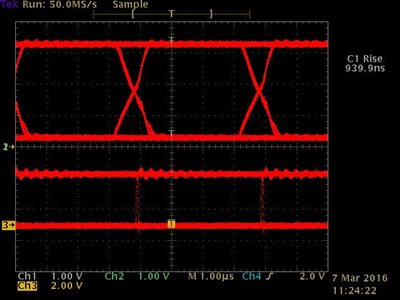
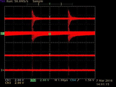
We have introduced a chip that signifies a leap forward in finding these signals: a new high-resolution, ultra-fast analog-to-digital converter (ADC), the ADC32RF45.

“We are enabling the next generation of these systems for high-resolution telescopes that can detect signals very far away,” said VC Kumar, product line manager. “These are extremely demanding systems because they are trying to detect a very small signal, determine what kind of signal it is and determine how far away it is. The sources of signals travel millions of light years and take time to get here.

“How you detect a weak signal accurately – that’s what we are enabling.”

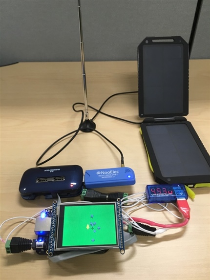
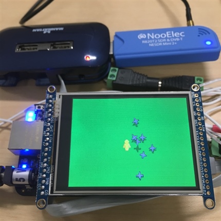
We began selling the evaluation module on TI.com this week, and we are working with radio-astronomy customers to enable advancements in their quests, VC said. “It is exciting, and we look forward to the results.”

Discoveries closer to home

Our device is also creating opportunities for closer-to-home discoveries in defense and aerospace, test and measurement and wireless communication systems.

Take radar systems, for example.

“If you have a radar system with this technology and you are aware of a small drone in your air space, you could see the drone sooner and take evasive action. You need a technology that can find something very small in the distance,” VC said. “We can enable customers to identify the sources of these signals quicker and more accurately, so they can react quicker.”

This innovation has several benefits for innovators the world over. For one, it helps them meet their requirements for larger bandwidth in next-generation systems and additionally enables smaller, portable form factors. It enables a direct RF signal conversion and allows engineers to connect with the highest dynamic range and input bandwidth. This means they can access a wider frequency range and get “cleaner data” without worrying about extraneous noise – so they can find the information they are looking for.

A wideband frequency is critical for military defense systems, VC said.

“For a radar system in military communications, you’re trying to monitor frequency bands to see if there is a signal there,” VC said. “With the ADC32RF45, you can sweep through these frequency ranges quickly. The more and faster you can see, the better.”

The device can even help the good guys stay one step ahead of the bad guys, he said.

“The bad guys are getting smarter,” he added. “Because we are able to provide our customers much better data quicker, they can then use their ‘secret sauce’ to build better military applications.”

VC likens a wideband frequency to a sophisticated security system in your home or business.

“You don’t want the cameras to have any blind spots – you need complete line of sight across each room in the entire house,” he said. “It’s the same concept with military communications.”

Sophisticated, yet simple


The data converter offers a simplified direct radio frequency sampling system architecture. In this architecture, the data converter digitizes a large chunk of frequency spectrum directly at the radio frequency and hands it off to a signal processor to dissect the information.

This is a paradigm shift that takes what has traditionally been handled by analog processing (mixers, local oscillators, filters and amplifiers) into the digital domain.

A new class of direct RF-sampling ADCs is being designed in advanced CMOS processes that allow much higher conversion rates with lower power than some previous generations. Combine this with a new serial communications interface, JESD204B, which TI has been in the forefront of defining – and we have a very size- and power-efficient digital interconnect between the data converter and digital processors.

“Traditional systems have many components to make them work. We have greatly simplified this ADC to make it easier to design with these other components,” VC said. “This meets engineers’ requirements for higher integration, better noise performance, wider bandwidth and smaller form factor.”


Size is important to designers, who want more devices packed into a single system so they can be more portable, VC said. Think vehicle and handheld radios for military personnel, satellites, airplanes and military vehicles.

“If we can help make these systems portable, our customers can take them anywhere,” he said, adding: “Our device has asmaller system footprint than any of our competitors’ devices.”

The ADC32RF45 helps reduce the RF footprint by 75 percent, said Joe Venable, a general manager in our High Performance Analog group.

“This allows customers to get to market faster by eliminating the ‘black magic’ tuning of the RF and IF stages,” he said. “Also, the quality of the system will increase with fewer components involved.” 

The converter is the industry’s fastest 14-bit ADC and extends our leadership in RF sampling.

“The ADC32RF45 represents a perfect marriage of ultimate bandwidth, lowest noise and highest dynamic range,” Joe said. “Its speed and resolving power is enabling designers to develop new applications, such as high-definition telescopes.”

But the TI team is not resting on its laurels. We are currently sampling a new ADC that can achieve even faster sample rates and bandwidth.

We plan to demonstrate the product next week at the International Microwave Symposium (IMS) in San Francisco, targeting defense and aerospace, wireless communications and test and measurement customers. Look for the device at booth No. 419.


Here’s what’s coming soon to a digital cinema near you

$
0
0
When it comes to innovations for the big screen, few people have a better picture of what’s next in cinema technology than our very own Dave Duncan. As the manager for our DLP® Enterprise and DLP Cinema® business , Dave has one foot in the...(read more)

Get Connected: How to operate your RS-485 links without termination

$
0
0

Welcome back to the “Get Connected” blog series on Analog Wire. In my previous post, I explored protecting your differential bus against system-level transients using a transient voltage suppressor (TVS) diode and pulse-proof resistors. In this post, I’ll take a look at the pros and cons of operating a RS-485 link without any termination on the bus.

Before diving into the topic of an unterminated RS-485 bus, let’s review the basics of traditional RS-485. The Telecommunications Industry Association/Electronic Industries Alliance (TIA/EIA)-485-A is a balanced data-transmission standard for serial communication. RS-485 provides robust serial data transmission at moderate data rates over long distances in multipoint communication applications. Traditionally, an RS-485 bus is connected in a daisy-chain fashion, supports up to 32 nodes on a single bus, has a 60Ω characteristic bus impedance and is terminated with a 120Ω resistor at each end of the network to match the characteristic impedance of the bus. Figure 1 shows a traditional half-duplex RS-485 bus topology. 

Figure 1: Traditional half-duplex RS-485 bus topology

Installing termination in the proper locations can be troublesome in applications like building automation, where you may not know the two farthest nodes. Additionally, the technician performing the installation may not have a clear understanding of termination, why it is important, or how unterminated stubs can lead to signal-integrity issues that cause network downtime.

The workaround for a problem like this is not to train all of the technicians in the world in the finer points of RS-485, but rather to eliminate the termination. Figure 2 shows an unterminated half-duplex RS-485 bus topology.

Figure 2: Unterminated half-duplex RS-485 bus topology

At this point, you may be asking how an RS-485 bus can operate successfully without termination. The answer is in the driver stage of the RS-485 transceiver. An RS-485 transceiver employs a full H-bridge output structure that is designed to drive a minimum of 1.5V differentially across a 54Ω load. The bus voltages for RS-485 are typically VOH = 3.5V and VOL = 1.5V, with a common-mode voltage (VCM) of 2.5V. This does vary from device to device, which is why these values are stated as typical.

When there is no termination present on the bus, the output stage of the transceiver still switches normally with the incoming data on the driver. But instead of swinging from the typical VOH and VOL, the output will swing full rail (from VCC to GND) minus a diode drop. The design of the output stage includes the diode for reverse-current protection on the device.

Nothing is free, though, and there is a drawback to eliminating termination on the RS-485 bus. When termination is removed, the entire bus acts essentially as a giant stub, causing bandwidth limitation in the design. Stubs on a bus cause reflections – and reflections cause signal-integrity issues that lead to data-communication errors. How long a stub can be in a design is not dependent on data rate, but rather the transition time from high to low and vice versa.

You can calculate the maximum stub length achievable in a design using Equation 1:

Where v is signal velocity of the cable as a factor of c (typically 78% for copper) and c is the speed of light. From Equation 1, you can see that the slower the transition time of the RS-485 transceiver, the longer the stub can be.

To illustrate the above point, I used the SN65HVD72 with a typical rise time (tr) of 700ns and the SN65HVD75 with a tr of 7ns. I tested both devices at 250kbps on a short bus (~8 inches) with a 10-foot stub. The 10-foot stub dominants the performance of this test case. Figure 3 depicts a visual representation of the topology used for this test case. Figures 4 and 5 below show the results from the SN65HVD72 and SN65HVD75 test case respectively.  

 Figure 3: Unterminated bus topology

Figure 4: SN65HVD72 output bus waveform

Figure 5: SN65HVD75 output bus waveform

From this test data, you can conclude that with careful selection of the RS-485 device, you can eliminate the termination resistors from some buses, and thus remove the need to know the farthest reaches of the bus. This takes the guesswork out of installation for technicians and ultimately accelerates the implementation of the end customer solution. Results will vary from design to design, as the type of bus topology (star network, cluster network design, or linear daisy chain) will play a factor in system performance.

Leave a comment below if you’d like to hear more about anything discussed in this post, or if there is an interface topic you’d like to see in the future. You can also subscribe to Analog Wire to receive an email notification upon the publication of the next post.

Additional resources

New proof-of-concept design shows health monitoring in a small form factor smart patch

$
0
0

Monitoring the basic functions of the human body can be useful to detect medical issues. Four vital signs are traditionally measured to keep track of these functions:

  • Temperature
  • Pulse
  • Respiration
  • Blood pressure

In many cases, these vital signs can be monitored using a microcontroller (MCU)-based system. While medical applications often require certification and the need to leverage specific algorithms to accurately monitor these vital signs, our new multi-parameter bio-signal monitor proof-of-concept shows how a system can use TI devices to measure three of the four primary vital signs described above. This ultra-low-power smart patch design can directly measure electrocardiogram (ECG), galvanic skin response (GSR) and skin temperature while also indirectly measuring other data such as step count or respiration rate.


This design demonstrates how a flexible substrate can be used with TI devices to adhere to skin to take the measurements. The patch will take in sensor data (ADS1292 ECG sub-circuit, LM4041 and LMP2231 GSR sub-circuit, TMP112 temperature sub-circuit and acceleration sensors) with algorithms running on the MSP430FR5989 microcontroller to derive health signs such as dehydration or ECG. It then leverages near field communication (NFC) as an interface from the patch to a smart phone (example app provided with design) to enable interface to the collected vitals.

To learn more about this TI Design reference design, download the design guide today!

Additional resources:

Improving road safety by the headlight: LED matrix manager

$
0
0

In my previous blog post, I introduced an automotive light-emitting-diodes (LED) headlight unit using switch-mode regulators. Those LED headlights are static; that is, they either turn on or off. You might turn on the fog lamps when the weather is bad or use your low beams at night and save your high beams when driving uphill. However, have you ever experienced a glare from a vehicle with its high beams turned on (as shown in Figure 1)? Such a glare can be quite dangerous, as it reduces your visibility.

Figure 1: Traditional front light technology

Wouldn’t it be superb if an intelligent system could detect vehicles in oncoming lanes and switch off some portion of that high beam (as shown in Figure 2)? Or if the light changed position according to the position of vehicles in oncoming lanes? In recent years, car manufacturers around the world have been investing in this area; some high-end vehicles are now even equipped with such technology. Let’s explore what’s inside these kinds of headlights.

Figure 2: Adaptive front lighting

An advanced driver assistance system (ADAS) includes cameras that detect images around the vehicle and provide real-time information to the vehicle’s central control system. The headlights comprise small pixels, which can individually turn on and off or change light intensity. A driver can feed the ADAS information to tell the headlights what to do according to the real-time location of an oncoming vehicle. This is the antiglaring function implemented in an adaptive headlight. An adaptive headlight can also turn beams or a welcome light electronically without motors.

At the end of 2014, TI released the TPS92661-Q1 LED matrix manager to help headlight manufacturers implement adaptive headlights. You can control 12 series LEDs by simply connecting all of them to the TPS92661-Q1. Running on a universal-asynchronous-receiver/transmitter (UART) protocol, an MCU can command the TPS92661-Q1 to control each LED pixel in the matrix. One UART system can connect up to eight TPS92661-Q1 devices (three physical address pins); therefore, the maximum number of pixels for an adaptive headlight is 96 pixels.

The device has 12 individual switches parallel to the LED, connected so the LED can turn on or off or be pulse-width modulation (PWM)-dimmed. The TPS92661-Q1 provides 10-bit PWM dimming resolution, or 1,024 steps of brightness control for each individual LED. Because all LEDs connect to the device individually, its open condition will be protected by shorting the switch in the device, and there is an internal register records fault upon the detection of an LED open or short.

A vehicle that incorporates adaptive LED headlights, enhances road safety and creates a welcomed, safe light? It’s definitely on my wish list.

Be sure to read other blogs on LED lighting.

Additional resources

Control-level design challenges in smart factory automation systems

$
0
0
Factory automation systems designed for Industry 4.0 typically contain three main levels of equipment that drive real-time communications and control: The field level where I/O modules, actuators, and drives are engaged in the physical operation...(read more)

DIY with TI: Plane spotter addresses drone safety concerns

$
0
0

At TI, we celebrate the makers and hobbyists who enjoy creating and innovating on their own time. In our ongoing DIY with TI series, we share their incredible Do It Yourself inventions using TI technology.

Jesse1Drones and quadcopters have captured the imagination of people, old and young, worldwide. These unmanned aircraft have also caught the attention of those who regulate air travel, as planes, helicopters and other aircraft now must share the sky. Concern over mid-air collisions is the inspiration behind the latest DIY with TI project from TIer Jesse Gronowski.

His inspiration actually stemmed from conversations with colleagues Alex Smith and Emma Betzig. When Alex needs a “brain break” from his work as a product test engineer, he typically stops by Jesse’s desk, who is also a test engineer.

“On a daily basis, we chat about products and bounce problems and solutions off each other. For me, he is almost like tech support, and it goes both ways,” Alex said.

These conversations inevitably led to the hobbyist world and the various TI MSP microcontroller (MCU) LaunchPad™ development kits and BeagleBone Blacks scattered on Jesse’s desk. One day, Alex mentioned to Jesse a technology called software defined radio (SDR). These radio modules plug into a USB port on a computer, enabling a person to tune into all different types of radio signal transmissions.

“I started looking into what I could do with this technology, and one of the most interesting things you can do is listen to airplane transponders and collect a lot of data including speed, heading and altitude,” Jesse said.  

Jesse also enjoys helping others who are new to the BeagleBone Black with their projects, like Emma, a process equipment engineer.  It was Emma who made the connection between one of Jesse’s other DIY projects and the SDR technology. 

“I am building my own quadcopter and Emma said, ‘This plane spotter project could be really good for flying your quadcopter and knowing what kind of aircraft are in the area.’”

With that, a DIY with TI project was born. While the radio signal technology worked well with a computer, Jesse wanted to be aware of other aircraft in real-time while flying his quadcopter. He chose the BeagleBone Black with the Sitara™ AM335x ARM® Cortex®-A8 processor as the backbone of his DIY with TI project, hooking up the board to the RTL-SDR module. The entire device connects to a screen with a map displaying the air traffic immediately in the area.

Jesse“There are apps you can get for your phone or tablet that attempt to do the same kind of thing, where the app displays the air traffic around you. But my device doesn’t need a cellular or data connection to the Internet or rely on others. It picks up the signals itself in real time with no delay,” Jesse said.

For Jason Kridner, the co-founder of the BeagleBone Black, it’s the kind of innovation for which he built the platform.

“I’m constantly in awe of the things people are creating with BeagleBone Black – from the perfect coffee machine to laser cutters to 3-D printers to dirty-dish detectors to plane spotters. Anything that you would want to make from electronics, someone has made it with BeagleBone Black,” Jason said.

Jesse plans on showing off his BeagleBone Black plane spotter next week at the annual DIY with TI event at our headquarters in Dallas. By participating in the event, he said he is attempting to solve the real-world problem of sharing airspace while also fulfilling a childhood dream.

“Ever since I was a kid, I wanted to have a remote-control airplane, but those kits were always too expensive and out of reach,” Jesse said. “With the technology that we produce at TI, it is making all those things much more economical. It is now within the reach of a hobbyist to be able to not just afford and buy components, but understand how they work, be able to put them together in your spare time and have real results you can enjoy.” 

No small matter: How to reduce voltage regulator size

$
0
0

My wife loves to get flowers. It is amazing how a simple, small gift can bring such a big smile to her face. The flowers brighten up our home and our spirits.

If only reducing voltage regulator size was such a small matter. There often seems to be more components to cram onto a circuit board than space available. More features and functions need to fit in a confined area. Higher levels of integration and Moore’s law have been effective at shrinking some devices but have had little impact on direct current (DC/DC) converter size. Power converters can easily consume 30% to 50% of overall system size. How do you get past this bottleneck?

One obvious answer is to increase operating frequency. Most point-of-load voltage regulators are switching converters using a buck (step-down) topology. Increasing switching frequency reduces the inductance and capacitance required to meet the regulator’s design specifications. Since inductors and capacitors usually take up most of the space in a DC/DC converter, as shown in Figure 1(a), this can be quite effective. But it’s not that simple. So what’s the catch?

Figure 1: Size comparison between a 12VIN, 10AOUT buck converter operating at 500kHz (a) and a series-capacitor buck converter operating at 2MHz per phase (b)

Blindly increasing frequency also increases power loss. Energy is lost every time a switching action occurs. Hence, switching loss scales proportionally with frequency. Conversion efficiency drops and heat dissipation can be a major problem. Frequency is limited to hundreds of kilohertz in most converters today. Those that do operate above 1MHz are typically low voltage (5V and below) and low current (less than 1A).

It’s time to “think outside the buck.” Buck converters have been the workhorse of the industry for decades but have fundamental limitations. We’re excited to introduce a new DC/DC converter topology optimized for high-voltage-conversion-ratio point-of-load applications. The series-capacitor buck converter enables multi-megahertz operation without compromising efficiency. As you can see in Figure 1(b), the reduction in total solution size is quite impressive. For the same input and output conditions as the buck converter in Figure 1(a), the series-capacitor buck converter based on the TPS54A20 is eight times smaller. That’s 1,270 mm3 vs. 157 mm3.

Figure 2: Height comparison between a 12VIN, 10AOUT buck converter operating at 500kHz (a) and a series-capacitor buck converter operating at 2MHz per phase (b)

Voltage regulator size reduction opens the door to new opportunities. Consider the height profiles shown in Figure 2. The conventional buck converter shown in Figure 2(a) is 4.8mm tall. This is well above the height limitation many systems have for their back-side components. The low profile of the series-capacitor buck converter (1.2mm tall) allows you to place the voltage regulator on the back side of your circuit board. This frees up valuable top-side real estate. It was not feasible before to fit an entire 10A converter on the back side – the passive components were too large. With the TPS54A20, now you can.

Additional resources


A much smaller boost converter for slightly smaller power banks

$
0
0

With smartphones and tablets growing in size every year, their battery capacities must also grow. Increasing the battery’s milliamp-hour (mAh) capacity provides the same or increased operating time at its operating power, which also increases with additional functionality and larger display sizes. If charged at the same rate as smaller-capacity batteries, these larger batteries take longer to fully charge. Consumers generally don’t like longer charging times, however, so higher-power converters are required to charge at faster rates. Higher-current battery chargers such as TI’s bq25890 and bq25898 family are a big part of delivering a fast-charging solution inside the smartphone or tablet.

When using a power bank, you also need a second battery charger for the power bank’s internal battery, as well as a high-power boost converter from the power bank’s internal battery to the power bank’s output connector (usually a USB port).  Most power bank chargers like the bq25895 have an integrated boost converter for USB – OTG capability.  But depending on the system requirements – for example if you need two independent output ports, or if you need higher charging currents or voltages – you need a separate higher-power boost converter.  The boost converter’s output voltage, which is normally 5V but can be set to 9V or 12V for some types of fast-charging systems then becomes the input voltage to the smartphone’s battery charger.  The charger in the phone needs to be capable of working with higher input voltage to take advantage of these features.

Both the phone’s battery charger and power bank’s boost converter need to be rated for higher output currents, which are sometimes above 4A. The TPS61088, fully-integrated synchronous boost converter, fulfills the boost need by providing up to 5A to the 5V rail at 95% efficiency, as shown in Figure 1. Such high efficiency creates little heat in the power bank and converts more of the power bank’s energy to output power, which then flows into the portable device’s battery. Generating less heat inside the power bank keeps the batteries at a safe temperature as well.

Figure 1: The TPS61088 provides 5A at 5V at 95% efficiency from a single-cell lithium-ion battery

But what if you’re not designing such a high-power power bank and don’t need 5A of output current? What if your power bank is just a little bit smaller and designed for recharging cameras, smaller smartphones or portable GPS devices? Then you don’t need the highest-power boost converter – a high-power one will do. With a lower-power boost converter, you can achieve a smaller size and lower cost. Meet the TPS61088’s little brother, the TPS61089. Figure 2 shows its efficiency – 90% when delivering its full 4A at 5V output power.

Figure 2: The TPS61089 provides 4A at 5V at 90% efficiency from a single-cell lithium-ion battery

Both boost converters are very similar: integrated MOSFETs with synchronous rectification enable high efficiencies, adjustable switching frequencies allow a trade-off between size and efficiency, and adjustable current limits allow you to scale your individual power-supply design to the specific needs of your application.

But each device is also different. The MOSFETs are different – smaller ones in the TPS61089 family enable a 2mm-by-2.5mm package but lower efficiency and less output power. Larger ones in the TPS61088 family enable the highest efficiency and highest output power (up to 30W), but also higher cost and a 3.5mm-by-4.5mm package size.

Either boost converter provides excellent size and efficiency for its power level, leaving the trade-off decisions to you. Which will you choose?

Additional resources


How to leverage the flexibility of an integrated ADC in an MCU for your design to outshine your competitor – part 2

$
0
0

In my recent posts, we’ve explored how to increase ADC performance by oversampling a 14-bit analog-to-digital converter (ADC) integrated into an MCU and discussed the key performance features that provide flexibility to your design. 

Today, I will focus on the ease-of-use- features of the MSP432P401R MCU’s 14-bit ADC, named ADC14, which offers the flexibility to customize for your application:

  • Ease-of-use features:
    • Choice of sample and conversion modes
    • Block process w/ DMA
    • Internal temperature sensor
    • Internal battery monitor
    • Window comparator
    • Interrupts

While utilizing the flexibility means the user needs to spend time to understand the features, some features are implemented to increase ease of use so there is pay back. 

Sample modes

The different sample modes support different application needs. The ADC14 can either be triggered by the SC bit or triggered with an on chip timer. Then, pulse sample mode allows ADC14SHT bits to control the number of clocks for the sample period. Or in extended sample mode the sample time is the duration of the sample trigger (such as on chip timer) being asserted. 

Conversion modes

Four modes conversion modes are offered to allow ADC to run without user input being required between multiple conversions.

There are thirty-two different ADC14MCTLx registers available to program a sequence of up-to 32 channels that get converted along with each ADC14MCTLx register being able to select the input channel to convert, single-ended or differential input mode, the reference to use, REF, and if a window comparator should be used along with whether to use threshold 0 or 1. User selects which ADCMCTLx register is the last one to be converted with the ADC14EOS bit or in case of repeat sequence of channels conversions continue until ADC14ENC bit is set to 0.

The flexibly of configuring a conversion sequence with each ADC12MCTLx register being able to independently select the input channel and its needs is great for applications using multiple input sensors with different needs such as fitness trackers where an accelerometer needs roughly 20 samples per second per axis but a temperature sensor only needs one to two samples per second.

The quickness of a sequence of conversions to take multiple back to back samples, in addition to the fast sample rate of the ADC, allows some applications such as test and measurement to use ADC14 for pseudo simultaneous samples.


Block processing with DMA

When ADC data needs to be processed in larger blocks than the 32 memory registers allow, the user can do block processing by utilizing the DMA to transfer data from the ADC memory registers. Using an interrupt to signal when data needs to be transferred from the ADC memory registers ADC14MEMx, the interrupt routine can request the DMA to transfer that data. Then, MCU can processor once DMA has transferred enough data.

Internal temperature sensor

Internal temperature sensoris available as an internal input to the ADC for user convenience.

Internal battery monitor

Internal battery monitoris available as an internal input to the ADC for user convenience. It can be setup with the window comparator to use an interrupt to alert when the battery reaches a certain threshold. Thus, no processor bandwidth needs to be used to constantly check the battery voltage of the ADC converted value.

Window comparator

A window comparator for low power monitoring of input signals of conversion-result registers is available. If window comparator is enabled in the ADC14MCTLx register, it checks for the converted result, which can be above ADC14HI, below ADC14LO, or within the two user programmed threshold and sets the corresponding interrupts. There are two sets of ADC14HI and ADC14LO registers to allow for different sets of thresholds for the different channels. The window comparator is a great way to be notified when the signal is in a range you care about and then adjust frequency and/or resolution of measurement to save power.

For example, for sound detection, such as glass breaking, ADC14 could be in 8-bit mode with window comparator looking for it to cross over a threshold to signal if a sound is made. When that happens, the ADC could switch to a higher resolution mode to do processing on that sound signal to determine if it was glass break. This application level partitioning of ADC performance needs is used to minimize energy used.

Interrupts

Each ADC14MEMx register has its owninterruptwhich along with the four conversion modes gives the user flexibility to not have to constantly monitor the ADC waiting for the converted result. The window comparator interrupts also offer the ability to monitor the value of the conversion register and then react when it gets in the desired range.

To get started, order our easy-to-use MSP432 MCU LaunchPad™ development kit.

If leveraging the 14-bit ADCs flexibility to optimize the power for your application is interesting – stay tuned for the next blog in this series where I will discuss low-power for ADC14 on MSP432 MCU!

Additional resources

Advantages of wide band gap materials in power electronics – part 1

$
0
0

With the introduction of new wide-bandgap materials such as gallium nitride (GaN) in transistor fabrication, significant figure-of-merit improvements translate into potential improvements in power supplies.

In this two-part series, I’ll discuss how these new wide-bandgap materials can benefit new designs.

Using newer materials that exhibit a higher bandgap than silicon-based semiconductors enables a reduction in die size while maintaining the same blocking voltage.

A smaller die results in lower parasitic capacitances and the lowering of both transistor gate charge (Qg) and output capacitance (Coss). This translates directly into faster transition speeds with less transition losses, less Coss dissipation and less driving Qg losses at a given frequency compared to classic silicon MOSFETs.

Whereas designers don’t drive silicon FETs in power applications above a few hundred kilohertz because the switching losses become prohibitively large, the lower parasitics enable GaN-based FETs to operate at frequencies up to 10 times higher while maintaining comparable switching and driving losses.

This ability to operate at higher frequencies lowers ripple voltage and current, which equates to lower conduction and magnetic-core losses, and a potential reduction in the size of inductive and capacitive components.

Advantages of high-frequency operation

With higher frequencies, the need to store energy in-between charging cycles is linearly reduced. Therefore, all passive components used for energy storage or filtering can be smaller.

Size-reduction benefits are especially evident in applications where size, weight and form factor are critical. For instance, in any application that is not stationary (such as for airborne or mobile systems), size and weight are major concerns, as more fuel is needed as weight increases.

A second advantage of shifting to higher frequencies is the reduction of the electromagnetic interference (EMI) filter: passive filters become more efficient at higher frequencies, and above 5MHz the switching noise generated imposed by standards (EN55022) relaxes by an extra 5dB. Higher frequencies are more likely to find a radiation path, however; Faraday shielding (available only on grounded systems) and careful layout become increasingly important.

Reducing component size

As frequency increases, voltage and current ripple decrease, thus reducing the required capacitance.

Large aluminum capacitors, which are very effective up to the lower hundreds of kilohertz, become ineffective once switching frequencies push into the megahertz realm. You can replace aluminum capacitors with compact ceramic capacitors, which exhibit lower impedances due to both the structure and connection method to the board.

Using ceramic capacitors requires that you pay attention to their self-resonance (most standard ceramic capacitors are good up to a few megahertz) and DC voltage bias. To counter these effects, select and carefully lay out lower-impedance form factors, and select high-grade dielectric material (NP0/C0G or X7R).

Similarly, you can reduce the size of inductors and transformers when increasing frequency, but the selection of magnetic materials that can maintain good performance at multiple megahertz with high changes in magnetic flux (dΦ/dt) (due to fast changing currents) is limited.

Above 5MHz, it is possible to get rid of the solid core and adopt air-core inductors. Air-core inductors remove core losses, but the lower permittivity of air forces a larger number of turns for a given inductance value. This results in higher copper losses and a construction that might be larger in volume than a solid-core solution, with strong fields radiating out further into space. Researchers are experimenting with higher-frequency magnetic materials that might be a good solution for multi-megahertz applications.

So what are the consequences of shrinking a power supply? I’ll explore this question in the next installment of this series.

Get to know TI GaN solutions and begin your design. 

Geek confessions: From geek-inspired love to a mind-controlled helicopter experiment

$
0
0

Geeks do things differently…and we’re glad they do. On Geek Pride Day, we celebrate geeks around the globe – what makes them tick, what makes them unique, what fuels their brilliance.

Today is a time to applaud those who take being a geek to the next level – as well as a time to acknowledge the geek in all of us. So in the spirit of geeking out, five TIers volunteered to share some of their geekiest confessions.

TI AvatarLeigh Price - Dallas, TX

Geekiest confession: I found love quoting Star Wars.

“I walked through a room and my boyfriend was watching a Star Wars movie. Without stopping, I recited the next line in the movie and kept walking. My boyfriend told everyone in the room, ‘I'm going to marry that woman.’ He proposed six months later and we've now been married for seven years.”


TI AvatarMark A. George - Sherman, TX

Geekiest confession:  I’m building a mind-controlled helicopter.

“After watching a show about a mind-controlled prosthetic device, I wanted to create the technology using something readily available and then adapt it to a prosthetic device later. I had a small electric helicopter at home so I started with a microcontroller, then wrote a program to take inputs from a keyboard and send them to the microcontroller, which the microcontroller then uses to adjust the digital potentiometer and fly the helicopter.

"I figure that I can build my own EEG using a data logger and some homemade active electrodes. If I can learn enough about the signals that I receive, maybe I can find a trigger in the signal to take place of the keystroke that flies the helicopter. Voila! Mind-controlled helicopter!”


TI AvatarEllen Hook - Virginia Beach, Virginia

Geekiest confession: I examine tensile strength…at the gym.

“While doing resistance training, I realized each color-coded rubber tube would provide a different resistance at the same elongation, and I wanted to know why. Upon dismantling the tubing from the wall, I could examine the tubes and feel the difference in the thickness of the different color-coded tubes. The resistance levels are determined by the larger diameter, the thickness of the tube. The thicker the tube, the more resistance it offered to an elongated stretch, the better the results for strength and fitness. Realizing I was talking out loud, explaining the results to anyone in ear shot, they asked, ‘Do you always want to know how things work?’ to which I replied, ‘yes.’ The whole gym was watching me!”


TI AvatarPál Bőle - Freising, Germany

Geekiest confession: I lost sleep building a 3D printer.

 “In college, I lived in a dorm with two friends who also enjoyed playing with electronics. One night, I found myself watching videos about home-built laser cutters on YouTube and something sparked inside me. I rushed to show my buddies and one of them said, ‘I have a broken inkjet printer here in the closet, let's use that!’ We instantly formed a team where each of us had a role to play: one started soldering a full-bridge DC motor driver, one started designing and implementing the control loop, and one started tearing the printer apart. By 5 a.m., the carriage which once held the inkjet head was moving according to our will! We had to use a lot of dirty hacks and some brute force, but the solution was fast, cheap, and it was at least doing something. But shortly after that someone made a short circuit, which caused the motor drive to go up in smoke. As we had no spare parts, we finally got to sleep.”


TI Avatar

Leara Webber - Portland, Maine

Geekiest confession: I crossed the Atlantic to meet “Dr. Who”.

“There have been many actors that have played the Doctor but my favorite is Tom Baker.  I found out he was going to be at a Tenth Planet event in Slough England, and my mom and I couldn't book the trip fast enough. I spent many hours making a K-9 purse to bring as a prop, and threw in a replica hat and scarf like the ones on the show. Somehow, the robot dog purse made it through security at the airport. The convention was crazy! My K-9 purse was a big hit. People took pictures of it and were surprised I traveled all the way from Maine. The highlight was definitely meeting Tom Baker and having him sign my handmade purse.”


Power Tips: Simple PSRR measurement with a frequency analyzer

$
0
0

The power supply rejection ratio (PSRR) is the power supply’s ability to reject ripple voltage applied at the input. This is normally done by adding a high-current power amplifier in series with the input source, driving it with a frequency-swept signal from a signal analyzer, and measuring the ratio of VIN to VOUT at each measured frequency. These power amplifiers are expensive, however, and easily damaged during testing. In this post, I’ll explain how to dispense with the power amplifier by repurposing a voltage-loop analyzer and making a few low-cost modifications.

Test setup

See Figure 1 below: I placed a small resistance in series with the input to apply a frequency-swept AC (Alternating Current) signal at VIN, injected by a signal transformer. The signal is actually applied across the small resistance. I placed three 0.15Ω resistors in series, each rated at 3W, to get 0.45Ω. I adjusted the input to achieve the target 3.3V at the DC/DC (Direct Current to Direct Current) converter input.

Figure 1: Test setup

I used a Venable 3120 frequency analyzer with “Bode boxes” and made some modifications.

Typically, the Bode boxes are set up to inject an isolated signal between V1 and V2, and to connect the V1 and V2 signals and ground from the converter under test to the V1 and V2 and ground inputs of the frequency analyzer. This enables one to measure loop gain with only three connections to the converter under test.

Using these same connections for both signal injection and measurement can introduce errors, however, as described in the post, “Power Tips: How connection wires affect Bode plot measurements.” Author Manjing Xie advises using the transformer connections only for injecting signals and having separate connections for measuring V1 and V2.

With PSRR measurements where VOUT is not connected to the injection transformer point, the V2 measurement would in any case need to be separate from the transformer connections. In my test, I injected signals through the Bode box, and had separate connections to measure both V1 (VIN) and V2 (VOUT).

I used the TPS40041 EVM – 001 evaluation module with one modification of R5 from 10k to 30.1k to change VOUT from 1.8V to 1.0V. Switching frequency was at 565-567kHz.

I tested at both no load and 2.6 A load off the 1.0V output.

I used the following generator settings and Bode boxes on the Venable 3120 for the different frequency ranges and took 20 points of data per frequency decade:

  • For the 100Hz to 1kHz range I used the 100Hz to 10kHz Bode box (model 200-002) and 1V RMS (Root Mean Square) out of the generator.
  • For the 1kHz to 100kHz range I used the 1kHz to 100kHz Bode box (model 200-003) and 1V RMS out of the generator.
  • For the 100kHz to 1MHz range I used the 1kHz to 100kHz Bode box (model 200-003) and 10V RMS out of the generator.

The PSRR results are shown below in Figure 2 for 2.6A load off the 1.0 VOUT and in Figure 3 for no load. The ratio of VOUT/VIN in is shown in red in dB (decibels). The phase relationship is shown in blue in degrees.

Figure 2: PSRR of modified TPS40041 EVM at a 2.6A load

Figure 3: PSRR of modified TPS40041 EVM at no load

Gain and phase patterns are very similar for no load and 2.6A load with attenuation slightly better at no load by about 3 dB at most.

The TPS40041 buck DC/DC controller does not have feed-forward input-voltage compensation in which the pulse-width modulator ramp is proportional to VIN to improve input-voltage rejection. For controllers with feed-forward compensation such as the TPS40170 PWM buck controller, you should expect an even more improved PSRR.

Now you should be able to eliminate the power amplifier by repurposing a voltage-loop analyzer and making a few low-cost modifications. Order the TPS40041 evaluation module or TPS40170 evaluation module and try conducting a similar test yourself.

Additional resources:

  • Explore more power-supply topics. Look under Power Supply Control Techniques as a good fast control loop will give the best PSRR performance.
  • Watch Power Tips videos to help with your design challenges.


eFuses: clamping and cutoff and auto retry, oh my! – part 2/3

$
0
0

If you missed part 1 of this blog series, be sure to check out the different options available with eFuses for handling overvoltage events (output-voltage clamping vs. output-voltage cutoff). In this installment, I’ll focus on eFuse options for overcurrent protection (current limiting vs. circuit breaking). Continuing our journey down the Yellow Brick Road, let’s once again start by delving into the more common option: current limiting.

The benefits of current limiting

When an overcurrent event occurs, an eFuse such as the TPS25940 will limit the output current to a threshold set by an external resistor. In Figure 1, when the eFuse sees 4A (assuming a current limit [ILIM] of 3A), it will proceed to limit the output current to 3A. The scope shot in Figure 2 shows this response, with ILIM = 3.6A. The eFuse will current limit until either the overcurrent event is removed (IIN< ILIM) or until the eFuse reaches thermal shutdown (typically TJ = 150°C). Once an eFuse enters thermal shutdown, it will enter one of two modes: either latch off or auto retry (both of which I’ll discuss in the third installment of this series).

Figure 1: TPS25940 current limiting 4A down to 3.6A

Current limiting shares similar benefits to that of output-voltage clamping, in that the eFuse allows the system to not see the overcurrent event, protecting all downstream circuitry from the higher current. It will also report the fault, allowing the system to prepare for imminent shutdown and perform “last-gasp” functionality. This can be beneficial in applications such as Solid State Drives (SSDs), especially if the overcurrent event is temporary. However, applications where safety is more important than uptime can benefit from an eFuse with circuit breaking instead of current limiting.

The benefits of circuit breaking

An eFuse with circuit breaking acts as its name suggests; it breaks the circuit in response to an overcurrent event. Looking again at Figure 1, if IIN suddenly became 4A, an eFuse with circuit-breaker functionality (such as the TPS25944A or TPS25944L) would open the circuit. This means that IOUT would be 0A, and all of the downstream circuitry would be protected from the higher current, as shown in Figure 2.

Figure 2: TPS25944A circuit-breaker functionality (IIN = 4A, IOUT = 0A)

The benefit of this functionality is similar to the benefit of an eFuse with output-voltage cutoff; it does not allow the higher current to affect any downstream circuitry. This form of protection comes at the cost of the downstream circuitry losing power, but that can actually be a good thing in an application like the inside of a data center server rack.

Imagine that the TPS25944A is protecting the input power to the hard drive, and the backplane connector shorts. If the hard drive has a current-limiting eFuse, it will continue to draw 3A through the backplane connector until the eFuse reaches thermal shutdown. This current draw through a faulty connector could cause the connector to overheat and begin to smoke or catch fire. If the hard drive contains sensitive data, it could be damaged in the resulting fire and the data could be lost.

There is no one-size-fits-all answer as to which type of overcurrent protection will be best for every application. However, now that you are familiar with what options are available, you should be able to make the best decision for your next design. Stay tuned for the third and final installment of this series, when I’ll discuss what happens after an eFuse enters thermal shutdown.

In the meantime, consider one of TI’s eFuse products to reduce system downtime and maintenance costs in your next design.

Additional resources


Push your receiver bandwidths past 1-GHz in high-end applications

$
0
0

** This is the 11th post in an Analog Wire RF-sampling blog series. **

I discussed the benefits of the radio frequency (RF) sampling architecture for wide-bandwidth systems in a previous post, however, the analog-to-digital converter (ADC) is often the limiting component for supporting large signal bandwidths in receiver systems. In this post, I will discuss how to push your wideband telecommunication systems past 1GHz.

Why do you need receivers capable of such wide bandwidths? For telecommunication service providers, wider bandwidths increase their system capacity and data throughput.They require improvements over existing systems, because the  number of cellular users is expected to exceed 5 billion by 2019. At the same time, users demand more data services to connect with social media, transfer work files, and stream video.

To meet customer demand, providers utilize carrier aggregation systems to spread signals across multiple bands in order to access additional bandwidth. 5G cellular systems will use wide-bandwidth signals in the microwave frequency bands, where a lot of unused spectrum is available.

Digital pre-distortion (DPD) feedback receivers also need large signal bandwidths. DPD generally requires an increase in the transmitted signal bandwidth to compensate for the third- and fifth-order intermodulation products generated in the power amplifier (PA). As transmittersignal bandwidth increases, the DPD signal bandwidth expands fivefold. An RF sampling ADC is the key component in all of these systems.

Yet bandwidth alone is not sufficient. High-end telecommunication systems require a high dynamic range. The receiver must handle both high- and low-signal levels.

Figure 1 illustrates a potential receiver spectrum with the desired frequency channel, along with a narrowband interferer and the transmitter bleedthrough signal. The interferer falls within the channel filter bandwidth; the ADC must handle that high signal without saturating. The duplexer filter and channel filter highly attenuate the transmitter signal – but since it starts out at a very high power level, it is still significant by the time it reaches the ADC input. If those interferers fall at the proper frequency, the intermodulation product lands right on the desired signal.

Additionally, the interferer’s high-order harmonics may fold back onto the desired channel. A high-linearity ADC with excellent spurious free dynamic range (SFDR) minimizes the degradation impact in these blocking scenarios.

Figure 1: Receiver interference spectrum

On the other end of the scale, you want a low noise floor to discern small signals from the noise. The noise figure of the system determines the receiver sensitivity. The sensitivity level is the lowest signal from which  the receiver can extract the desired information. The ADC’s signal-to-noise ratio (SNR) indicates the noise level in relation to a high input signal (usually near full-scale input). The absolute noise power density with a low-level signal indicates the device’s minimum noise-floor limit.

The thermal noise performance of the device is fixed. There is also noise contribution from the clock jitter. The total jitter is the root mean square (RMS) of the external clock jitter and the aperture jitter as seen in equation 1.  The aperture jitter is fixed and is inherent to the device; the value is extracted from the device’s datasheet.  The clock jitter depends on the designer’s external clock choice.  Implementing a low jitter clock solution is critical for good SNR performance. Equation 2 expresses how jitter impacts SNR:

Notice that the sampling frequency is not part of the equation, however, the input frequency is included. RF sampling converters are not inherently more sensitive to clock jitter, but because they operate at higher frequencies, clock jitter becomes a key factor in SNR performance.

There is a need to support the dynamic range of high-end receiver systems and very wide signal bandwidths. The TI Designs 1-GHz Signal Bandwidth RF Sampling Receiver Reference Design (TIDA-01161) showcases a solution for a 1GHz bandwidth signal suitable for stringent telecommunication standards. The ADC32RF45 is a 14-bit, dual-channel, 3GSPS ADC. It has a 3dB input bandwidth of 3GHz and samples input signals up to 4GHz. The device supports signal bandwidths of over 1GHz (up to 1.5GHz maximum).

Figure 2 shows a captured 1GHz-wide signal. The signal includes a total of 40 20MHz-wide cellular long term evolution (LTE) carriers (4G) centered at 2.2GHz. Four groups are separated by about 65MHz, with 10 carriers per group. The entire signal-bandwidth power is about -30dBFS. Notice that the spectrum is quite clean and that the noise floor is about -100dBFS, which is limited by the input signal’s noise.

Figure 2: 1GHz-wide signal bandwidth captured by the ADC32RF45 ADC

This reference design uses both the ADC32RF45 and the LMX2582 RF synthesizer for the ADC clock. The LMX2582 achieves a phase noise of -140dBc/Hz at 3GHz. This performance rivals test equipment and is suitable as a clock source for high-end RF sampling converters. This system is usable for wireless infrastructure base station receivers, large radar antenna arrays, high-end test equipment and DPD feedback receivers.

Next generation receivers need high dynamic range and large bandwidth capabilities to meet the growing capacity demands and the increase in data services.  The RF sampling architecture meets those requirements, while effectively integrating the functions of several other blocks which compacts the design.  This translates to lower cost and easier to design systems. 

Check back next month when I discuss the RF sampling advantages when using integrated digital down converters.

Additional resources


Where should I place my battery’s gas gauge?

$
0
0

Imagine for a second how useful (or useless) your car would be without a gas gauge. Not very appealing, is it? The same principle applies to battery-powered systems. Including a gas gauge in a battery-powered system provides accurate capacity information and helps extend the runtime of the application.

TI provides multiple solutions for single- and multi-cell applications, with gauging algorithms such as Impedance Track™  and Compensated End-of-Discharge Voltage, CEDV. But where should you place the gauge?

When designing with gas gauges, the designer needs to choose the cell count, chemistry and whether to place the gauge inside the battery pack or on the system board. Each alternative has advantages and trade-offs, depending on the application.


Figure 1. Pack-side and System-side configurations 

Gauges have typically resided inside battery packs. This configuration allows the gauge to monitor the battery continuously without losing power and to provide constant feedback to the system host about battery status. Another benefit of integrating the gauge inside the battery pack is the ability for the gauge to log lifetime data about the battery (similar to a black box) to help diagnose packs for warranty or troubleshoot any erratic behavior.

Since the gauge is integrated, it is able to be optimized to a particular cell model. But since the gauge is always on, it also acts as a constant load on the battery itself; TI battery gas gauges include low-power modes to help alleviate the gauge’s impact on battery runtime. Security measures can also authenticate battery packs and ensure packs optimized for the application are used.

For applications where you want to give consumers the ability to swap battery packs but still want to provide high-accuracy gauging information, consider system-side gauges. These gauges reside on the system board; they can detect battery-pack insertion events and quickly estimate the initial capacity and runtime of an inserted pack. They also provide more general purpose input-output, GPIO functions to make host communication more efficient via interrupts and decreased polling.

Regardless of your application, there are options available to integrate gas gauging in your battery-powered systems. A quick pros and cons analysis can help you choose which gauge is a good fit for your next project. For more details about gas-gauge selection, read “Selecting an Impedance Track Gas Gauge for Li-Ion Single Cell Applications

Additional resources

How low can you go? How to reduce power consumption in data-acquisition systems

$
0
0

When trying to reduce system power consumption, one method is to look for devices to optimize or remove. Another method is to evaluate the system as a whole and optimize for system functionality before evaluating at the component level. In this post, I’ll go over design techniques using low-power analog components that can help optimize overall system power consumption.

Add an external ADC to reduce overall system power consumption

In low-power data-acquisition systems, integrating an analog-to-digital converter (ADC) into the controller reduces overall component count, cost and ideally power consumption. But this approach may actually increase overall power consumption.

When sampling at 1kSPS, the typical power consumption of integrated ADCs in several low-power microcontrollers (MCUs) is often greater than the power consumption of a discrete ADC (Figure 1).Therefore, you can actually reduce overall system power consumption by placing the ADS7042 external to the microcontroller and turning off the microcontroller’s integrated ADC.  In fact, TI’s ADS7042 ultra-low-power 12-bit ADC consumes only 234nW of power when sampling at 1kSPS.

Figure 1: Power consumption of integrated ADCs vs. the ADS7042 at 1kSPS

An added benefit of using a discrete ADC instead of an integrated ADC is that you can keep the converter near the sensor signal to minimize noise pickup. A discrete ADC can also help expand the number of analog input channels that the microcontroller can support.

One concern with adding a device to save power is the amount of required board area for the discrete device. The ADS7042’s 1.5mm-by-1.5mm 8-pin quad flat no-lead (QFN) package is smaller than a standard 0805 surface-mount component, thus minimizing the impact to overall system-design size. In addition, the low pin count helps minimize routing during layout.

Examining a low-power data acquisition system circuit

Regardless of which type of ADC you ultimately choose for a low-power data-acquisition system, it is important to understand how to optimize the circuitry around the ADC to reduce overall power consumption. The main components in a data- acquisition system are the sensor input, the buffer to drive the sensor signal into the ADC, the ADC and the power source for the ADC.

An example of a low-power data acquisition system is showcased on the ADS7042 BoosterPack, which is a development board compatible with the TI LaunchPad™ development kit ecosystem. The circuit on the ADS7042 BoosterPack is designed to convert analog data from either an on-board ambient light sensor or a subminiature version A (SMA) connector (Figure 2).

Figure 2: Circuit diagram for analog input signals on the ADS7042 BoosterPack

When converting an external sensor input from an analog sensor source connected to the SMA connector buffered by the OPA316, the driver consumes 400µA of current at 3.3V, which results in 1.32mW of power consumption. This accounts for roughly 65% of the overall system power – which includes the power of the REFE3330 voltage reference (12.87µW) and the power of the ADS7042 ADC (690µW). If the sensor is directly connected to the ADC without the additional driver, as with the on-board ambient light sensor, the sensor circuit consumes only 99µW of power. This is 7.5% of the power consumed by the OPA316 in the first implementation of the circuit, without even taking into account the power required to drive the analog input-signal source (Table 1).

 Table 1: Circuit power consumption of the ADS7042 BoosterPack 

Reducing the need for the driver can help reduce overall power consumption. However, there are obvious trade-offs to using this solution. You must reduce the sampling rate of the ADC to maximize the settling time for the input sampling capacitor (CSH). But this has the advantage of also reducing the sampling rate and the power consumption of the ADC, as the converter’s power consumption scales linearly with the sampling rate (Figure 3).

Figure 3: Power consumption of the ADS7042 vs. sampling rate

When using the slowest sampling rate, 1kSPS, the throughput of the system is less than or equal to the sampling rate of the ADC, shown in Equation 1:

The input bandwidth is also limited by the sampling rate in accordance with the Nyquist-Shannon sampling theorem. Therefore, the input bandwidth is less than or equal to 500Hz, or half of the sampling rate (Equation 2): 

In addition to removing the need for the buffer, a lower sampling rate will also reduce the power consumption of the ADC.

Finally, the design will exhibit a slow transient response time related to the bandwidth of the system.  The response time is equal to the inverse of the input bandwidth or in this case 3ms, shown in Equation 3.

In this example, the use of an external discrete ADC helped reduce overall system power consumption. What is your experience with low-power system designs? Please log in and share your thoughts on low-power system design approaches in the comments.

Additional resources

Thinking beyond the buck controller for high-output power supplies

$
0
0

Choosing the right buck-converter topology for a battery-connected automotive power supply is usually pretty straightforward. For currents up to ~3.5A, a synchronous buck converter is the best choice. A buck converter with an integrated MOSFET half bridge requires less space on the printed circuit board (PCB), fewer external components and a lower bill-of-materials cost. The synchronous design is good for efficiency and lower power dissipation, especially at higher currents.

But a buck converter is not the best choice if you need output currents higher than 3.5A because of the increasing power loss and induced rapid temperature increase. The integrated MOSFET half bridge is located on the same die as the control logic of the buck. External MOSFETs are larger and have mostly better technical characteristics, like a very low on-resistance and gate charge compared to the small integrated FETs in a buck converter.

The best choice for higher output currents is to use a buck controller with an external MOSFET half bridge to reduce the losses mentioned in the section above. Choose the MOSFETs separately from the controller so that you can scale them to your power supply’s output-power needs. The power dissipation will spread widely over the FETs and the controller, which means lower temperatures on each device. With a buck-controller topology’s flexibility, you can meet a wide range of output-power needs.

Modern applications like automotive infotainment systems are based on very powerful processors, like the Jacinto 7 from Texas Instruments. As an example, the maximum output power for the Intel Apollo Lake processor is about 40W to 50W. A power supply connected at the car battery (VIN = 3.5V to 18V, absolute maximum 42V and VOUT = 3.3V) must be able to support output currents between 8A to 12A. Most engineers would choose a buck controller to handle the high-output power requirements.

One disadvantage of a buck controller compared to a buck converter is the significantly larger current loop between the MOSFET half bridge and the external components. Larger external FETs have lower losses; the size of the package allows a better thermal connection to dissipate heat, but they are by decades larger compared to an integrated half bridge in a buck converter. The larger current loop induces parasitic effects that will result in ringing on the switch node of the power supply.

Another disadvantage of the buck-controller topology – especially when it comes to high output currents – is the fact that discrete FETs are separately packaged and have large parasitic components, like serial inductors on the drain and source. Figure 1 shows a MOSFET half-bridge equivalent circuit with parasitic inductors on the drain and source.

Figure 1:MOSFET half bridge with parasitic inductors LDrain and LSource

The discrete FET parasitic inductors LSource and LDrain have the most significant impact on switch-node ringing and determine the ringing frequency. When the output current increases, the ringing will cause noticeable radiated electromagnetic interference (EMI). Figure 2 shows the ringing on the rising edge of the switch node of a synchronous buck controller. Figure 3 is an enlarged picture of the rising edge of the switch node. The ringing frequency is about 215MHz and is typical for a discrete packaged MOSFET.

The radiated EMI, especially in the region of about 200MHz, is unacceptable for applications like sensitive digital radio tuners (174MHz to 230MHz) or TV tuners in automotive infotainment systems.

Figure 2:Switch node of a synchronous buck controller. Note the ringing on the rising edge. Bridge based on a dual N-FET BUK9K17-60E.


Figure 3:Close-up of the rising edge of the switch node of a synchronous buck controller with a measured ringing frequency of about 215MHz

A new buck-converter topology for high-output power requirements

So what kind of power concept should you use in an EMI-sensitive, high-power-output application? A buck converter can’t handle the output power, and a buck controller causes significant radiated EMI with increasing output currents.

One idea is to use a single buck converter stackable to multiphase systems. The number of stacked devices depends on the maximum output current. Parasitic elements are reduced to a minimum and the power dissipation separates into multiple devices. This concept is very flexible and allows you to expand or reduce the system depending on the output current. The disadvantage is the large PCB space needed for multiple devices.

To enable this kind of topology, you will need a buck converter with an integrated load-share controller, phase synchronization – and ideally phase-shifting capability, such as the TPS54020, LM20154 and LP8754 Device Family. Figure 4 shows such a power-supply concept.

Figure 4:A high-output-power buck converter based on a multiphase system

In conclusion, we can determine that a buck controller with external FET is not the only solution for high current power supplies in EMI-sensitive automotive infotainment systems. Using a highly integrated buck converter in a multi-phase configuration overcomes the output current limitation and provides very good EMI behavior due to the integrated MOSFET half bridge.

Additional resources:

Tapping the cloud for IoT sensing solutions

$
0
0
The Internet of Things (IoT) is linking people, devices and cloud data storage services at an unprecedented rate. By 2020, some analysts estimate 50 billion digital devices will be connected to the Internet. Customers are leveraging DLP® Products...(read more)

An introduction to the Internet of Things

$
0
0

By now, it’s common to hear conversations about the Internet of Things (IoT), but why? Why is there so much buzz around the IoT?

What is the IoT? 

The IoT is an enabling technology with the ability to impact nearly everything we do and how we do it. It will allow for decision making on a much larger scale than ever before. Being able to control all of the machines in a factory or all of the street lights in a city, empowers  operators to make more educated decisions that weren’t previously possible on a small, local view – thereby driving increased efficiency as well as safety and security. The IoT enables original equipment manufacturers (OEMs) to unlock new revenue from existing products and services. OEMs can stay connected with their product as it is being used in the field and develop new services to add value based on the ways the product is being used. This is only one of many changes that the IoT may bring in existing business models and strategies. 

The Internet of Things is an expansion of the “Internet of people” brought about by the revolution of personal computers and cell phones connected to the Internet. Because of this mass adoption of the Internet as the means for providing services to people, the door has been opened to connect many more “things” to the Internet and leverage the same infrastructure and services. The IoT is an end-to-end process that connects these “things,” – products that include sensors and actuators – to gateways that can then transmit data to the cloud. The IoT connects the physical world, as perceived by the sensors and driven by the actuators, with the cyber world running in the cloud. It enables users to sense, store, present and analyze data to make informed decisions and help them to control the world around them.

Considerations and challenges

While the Internet of Things brings a new horizon of opportunities, there are several barriers in respect to making IoT implementations successful. Determining the use case – whether industrial, automotive, home automation, personal electronics or others – and the intended user benefit, will help developers make more informed design decisions. There are many practical tradeoffs and challenges in the nodes themselves such as deciding between a wired or wireless connection and whether to go with a plug-in, battery-powered or energy harvesting solution, while additional considerations may be related to the required processing performance for functions like calibration, signal conditioning or even local analytics, and the needed industrial robustness. The communication function has always been a barrier and this is especially true if we expect many new players to leverage IoT. To assist these OEMs, the communication function and software stacks have to be encapsulated and pre-certified. There are also end-to-end challenges to consider, with security being the most paramount. When deploying an IoT system, you’ll need a solution that spans from the sensor to the cloud and everything in-between. The challenge here is that this requires partnerships as no one company is able to address all of these elements by itself.

Texas Instruments (TI) is addressing these challenges by providing many of the building blocks for the IoT. We have a focus on embedded and analog devices and provide solutions for sensing, signal chain, power, processing and wired and wireless connectivity – everything you need to get from the node to the gateway to the cloud. Our focus in connectivity has been around reducing the complexity by providing a complete preinstalled and encapsulated Internet software stack. We also provide devices that are oriented specifically for industrial and automotive applications to address the needs in those integral areas of the IoT. TI has an extensive network of cloud partners which allow developers to quickly and easily connect their designs to the IoT while offering differentiated and value-added services.

Ask TI your questions during our Twitter chat 

Now that you have a baseline for what the Internet of Things is, we invite you to join our IoT Twitter chat. You’ll be able to talk about the IoT with some of our experts in real-time. Ask them your IoT questions, talk about trends and let us know what you think is coming next. Join the conversation on Twitter, June 1 from 8:00-9:30 a.m. CST, and tweet your IoT questions to @TXInstruments.

Learn more about the IoT

In addition to the Twitter chat, TI is celebrating the IoT during the week of May 29. We’ll be talking about the IoT all week as well as highlighting related topics. Be sure to follow our social channels all week and look for #IoTWeek to be a part of the conversation.

Key resources, including additional blogs and white papers, can be found below:

Viewing all 4543 articles
Browse latest View live


<script src="https://jsc.adskeeper.com/r/s/rssing.com.1596347.js" async> </script>