Quantcast
Channel: TI E2E support forums
Viewing all 4543 articles
Browse latest View live

Protect automotive USB circuits against short-to-battery faults – part 1

$
0
0

Vehicle manufacturers continue to make infotainment systems an extension of the multimedia experience. The USB interface has been a fundamental element of the infotainment architecture, and thus manufacturers have subjected this originally consumer-focused interface to significantly more stringent protection requirements. Among these is the need to protect against shorts to the vehicle battery that can occur during assembly, manufacturing or maintenance. For example, a damaged long-wire harness connecting the head unit to different connectivity modules can short all pins to the main 12V car battery. Other potential failure mechanisms include the use of noncompliant adapters, cables or chargers; mechanical twists of USB connectors or cables; or any sort of debris getting into the connector and shorting the data lines to VBUS.

In part one of this two-part series, I will illustrate the best way to protect USB circuits from short-to-battery faults. In my next post, I will expand on the best way to optimize your automotive USB short-to-battery design.

When designing for USB short-to-battery protection, always keep in mind three major areas:

  • The bandwidth of the protection solution.
  • The clamping voltage and response-time behavior.
  • The overcurrent and short-to-ground characteristics.

In the past, it wasn’t possible to find a USB 2.0 short-to-battery solution that could address all three areas, but TI’s new TPD3S714-Q1 family of short-to-battery protection devices can help solve these common issues.

Bandwidth

Signal integrity is one of the biggest challenges for design engineers working in automotive USB applications. Since USB 2.0 supports data rates up to 480Mbps, any small amount of capacitance added to the lines can distort the signal and cause failures in data transmission. Designers are left with the complicated task of finding a solution that will protect sensitive electronics against high voltage and current spikes, while maintaining optimal signal integrity.

The TPD3S714-Q1 is a single-chip solution for short-to-battery, short-circuit and electrostatic discharge (ESD) protection for the USB connector’s VBUS and data lines. The integrated data switches provide two times higher bandwidth for minimal signal degradation while simultaneously providing up to 18V short-to-battery protection. Figure 1 is an insertion-loss diagram highlighting the high-speed data switches with 1GHz -3dB bandwidth.

Figure 1: TPD3S714-Q1 data switch differential bandwidth

You can use eye diagrams to analyze line-capacitance effects on bandwidth. Measuring the minimum and maximum voltage levels as well as jitter makes it possible to expose any issues in USB data-line transmissions. The high 1GHz bandwidth allows for USB 2.0 high-speed applications. Extra margin in bandwidth above 720MHz also helps maintain a clean USB 2.0 eye diagram with the long captive cables common in automotive USB environments. Figure 2 is an example USB 2.0 eye diagram.

Figure 2: USB 2.0 eye diagram with the TPD3S714-Q1

Clamping voltage and response time

Even though bandwidth is one of the most important characteristics to keep in mind when selecting a protection solution, you also have to ensure that the clamping voltage is low enough to protect the downstream circuitry from any short-to-battery or ESD event. Furthermore, you should design the overvoltage field-effect transistors (FETs) to have a fast turn-off time in order to protect the upstream system-on-chip (SoC) from harmful voltage and current spikes as quickly as possible.

The short-to-battery protection isolates the internal system circuits from any overvoltage conditions at the VBUS, D+ and D- pins. On these pins, the TPD3S714-Q1 can handle overvoltages up to 18V for hot-plug and DC events. The overvoltage-protection circuit provides the most reliable short-to-battery isolation in the industry, helping improve system-level protection. Figure 3 shows its 5V clamping voltage during a short-to-18V fault, highlighting the ultra-fast response time of 200ns on the data path.

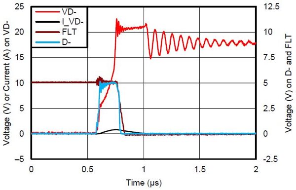
Figure 3: TPD3S714-Q1 data switch short-to-18V response waveform

Overcurrent and short-to-ground

Selecting a poor overcurrent-protection circuit can become a roadblock for faster time to market. Substantial amounts of current flowing through the system side during overcurrent events could cause a brownout or blackout to the upstream 5V rail and potentially bring down or reset multiple integrated circuits (ICs) connected to the shared rail. The purpose of an overcurrent-protection device is to limit the amount of current a USB port can draw, such as in a short-to-ground scenario. Furthermore, the USB 2.0 specification requires the use of an overcurrent-protection device in any USB Power Delivery design.

Figure 4 illustrates a short-to-ground event where the system voltage drops by less than 200mV, keeping the shared 5V rail stable and properly isolated from faults. The TPD3S714-Q1 integrates an accurate current-limit load switch up to 0.5A, automatically limiting current during an overcurrent event. The internal FET switch prevents excess current from flowing through the upstream device, keeping the system side from resetting.

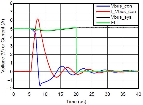
Figure 4: TPD3S714-Q1VBUS short-to-ground response waveform

Remember – when looking for a USB 2.0 short-to-battery solution, always keep in mind the bandwidth of the protection device, the clamping voltage and response time, and the overcurrent and short-to-ground characteristics. Considering these key areas makes implementations easier and reduces time to market for original equipment manufacturers (OEMs).

Subscribe to Behind the Wheel to receive an email notification upon the publication of the second post.

Additional resources


Voltage regulator features – inside the black box

$
0
0

As I travel and meet with customers across many market sectors, I have come to realize that many hardware designers become power-supply engineers by necessity. Hardware designers are responsible for designing voltage regulators that remain electrically and thermally stable under operating and expected worst-case conditions; meet the required power specifications of processors, application-specific integrated circuits (ASICs), double-data-rate (DDR) memory, hybrid cube memory and field-programmable gate arrays (FPGAs); and generate low electromagnetic interference (EMI). The job of a voltage regulator is to keep its output voltage constant (regulated) though line (input voltage), load (output current) and environmental variations.

Step-down (buck) voltage regulators are the most commonly used switching-regulator topology. Several voltage regulators are typically found in boards used in wired/wireless communication, enterprise server/storage, industrial and personal electronics. Today’s switching-voltage regulators have a plethora of control and protection features to ensure power-supply protection, reliability and output-voltage tolerance.

Let’s review some of their features.

•  Power good and enable: Power good is an output flag that indicates if the voltage regulator’s output voltage is within a pre-determined/programmed output-voltage window. Once the voltage reaches that window, it is on its way to the final programmed value, which is a good sign. Power good can be an active high or low signal.

Enable is an on/off input signal that can also be active high or low. Enable turns the voltage regulator on or off. If the voltage regulator has soft start, it will start in soft start, assuming that its input voltage is above the undervoltage lockout (UVL) threshold. If there’s a delay from the enable signal to soft start, the regulator will soft start after that time delay.

Power good and enable are often used for sequential power sequencing of multiple power supplies on the same board as shown in Fig.1

Figure 1: Power good and enable for power sequencing

  • Soft start: Soft start turns the voltage regulator on slowly to the programmed duty cycle and output voltage so that output current ramps slowly, reducing inrush current as shown in Fig.2. Inrush current  could cause output-voltage overshoot and a system glitch or damaged power stage. Inrush current happens when a board’s bulk capacitors are discharged and must then charge all at once when input power is present. Soft start also avoids current limits that could shut the DC/DC converter down (latch off). Soft start is usually adjustable or selectable through an external capacitor or a pin-strap setting (connecting the soft-start pin to existing voltage rails on the board).

Figure 2: The soft start of a voltage regulator and corresponding soft-start current (output)

  • Frequency synchronization: Frequency synchronization refers to the voltage regulator’s internal oscillator (clock) synchronizing to an external clock and switching frequency to match that of the external clock’s switching frequencyy. This is especially beneficial when more than one voltage regulator is present on the same board. Their fundamental switching frequencies can generate harmonics, which can then can generate beat frequencies that can make their way to the output in the form of noise if the audio rejection and filtering are poor as shown in Fig.3. Frequency synchronization is great for radio frequency (RF) or data-acquistion applications like base stations and medical imaging.

 Figure 3: Frequency synchronization

•  Pre-bias operation. A pre-bias startup condition occurs as a result of the presence of an external voltage at the output of a voltage regulator before that output becomes active. This is typically due to leakage currents in ASICs and processors that charge the output even after power down. When the regulator is enabled, it soft starts the high-side (switching) FET and its duty cycle ramps from zero to the required duty cycle for voltage regulation. If during soft start the synchronous FET is on when the high-side FET is off, the synchronous FET sinks current from the output by discharging the output capacitors through the inductor, causing the core voltage to drop and potentially causing the power supply to shut down.

A voltage regulator with pre-biased capability will disable full synchronous rectification (holding the low side off) during initial soft start, start the first low-side FET on pulses with a narrow on-time, and then incrementally increase that on time cycle by cycle until it coincides with the time dictated by (1-D), where D is the buck regulator duty cycle. Essentially, pulse-width modulation (PWM) pulses start when the error-amplifier soft-start input voltage rises above the programmed feedback voltage value (Figure 4). This ensures that the output capacitors do not discharge during soft start. Pre-bias relies on the input voltage being always higher than the output voltage. The output-inductor current sources current to charge the output capacitors only until the output voltage reaches the regulation value.

Figure 4: MOSFET drivers at beginning of soft start under pre-biased VOUT

Figure 5 shows startup waveforms of a 1.2V VOUT voltage under different pre-bias scenarios. The first trace is when the output voltage starts with zero pre-bias. The pre-bias levels of the second and third traces are 0.5V and 1.0V, respectively. When a pre-biased voltage is present at the output, the regulator will begin soft start from that voltage level onwards. TI buck regulators like the TPS53317A have pre-biased startup capability.


Figure 5: Voltage regulator startup waveforms under pre-biased VOUT

Understanding voltage-regulator features can demystify the idea that power supplies are an opaque black box. In future posts, I will look at other voltage-regulator features and how they relate to power-supply design and performance.

Downtown or the suburbs? Considering converters or controllers for high-current voltage regulation

$
0
0

Residents seeking more space generally give up living near downtown areas, with their likely proximity to work and city services, and move to the suburbs for bigger homes and spacious yards. Similarly, when engineers require higher currents for their point of load (POL) designs, they generally give up the conveniences of high-density converters (with integrated MOSFETs) and instead use a more sprawling solution involving controllers (with external MOSFETs). Controllers, like the suburbs, can offer relative flexibility and affordability, but take up more real estate – more board space, that is.

Until recently, applications requiring currents in excess of 10-15A generally relied on controllers with external MOSFETs. Converters – while enabling simpler designs with easier layout, fewer components in their bill of materials (BOM) and higher-density solutions with high reliability – traditionally delivered only a limited amount of power.

Applications such as network routers, switches, enterprise servers and embedded industrial systems are increasingly power-hungry – requiring 20A, 30A, 40A or more for their POL design. Yet these applications are extremely space-constrained and it is difficult to accommodate solutions involving controllers and external MOSFETs. The question is, how do you use converters rather than controllers in an application with large current requirements?

The answer primarily lies in recent advancements in MOSFET and packaging technologies. New-generation MOSFETs like TI’s NexFET™ power MOSFET offer lower resistivity (Rdson) in a given silicon area for higher current capability. PowerStack™ packaging technology stacks the integrated circuit (IC) and MOSFETs on top of one another – resembling a downtown building – to pack more in a given footprint.

Figure 1: Controller IC and MOSFETs vertically stacked in the PowerStack package

The unique combination of die stacking and clip bonding in PowerStack packages results in a more integrated quad flat no-lead (QFN) solution that delivers a smaller size, better thermal performance and higher current capabilities over traditional solutions that place MOSFETs side by side.

With recent advances in MOSFET and packaging technologies, TI now offers the option of using converters - with integrated FETs - for high-power, high-density POL applications. The TPS548D22 joins TI’s family of high-current synchronous SWIFT™ DC/DC buck converters to deliver up to 40A of continuous current and is offered in a 40-pin 5mm-by-7mm-by-1.5mm stack-clipped QFN PowerStack package.  Visit the DC/DC portal for the comprehensive TI offering.  Those of you who had to move to the suburbs can now consider moving back downtown! 

Out of Office: Finding inspiration in those who smile through hard times

$
0
0

TIer Marshall Worrall meets happy people in unlikely places, and that helps him keep life in perspective.

MarshallWhether he’s volunteering at Children’s Health℠, a local children’s hospital, or trekking among the peaks of Nepal, he’s struck by how happy some people seem, even when life is hard.

“It’s easy for me to get carried away with the activities and stresses of daily life. I find that spending time volunteering and experiencing new cultures helps me maintain my priorities,” he said. “Spending time after work at the hospital has been a great learning experience. I get to see the good with the bad. Those kids and families go through a lot. It feels good to help with that, as much as I can.”

An important perspective

Two years ago, Marshall – a mechanical engineer who leads a team that works on equipment in our manufacturing and test facilities – decided to give back to his community.

Marshall grew up in Dallas, and his parents have been committed volunteers for many years. He went online and learned about volunteer needs at Children’s Health, then went through the hospital’s vetting and training process and began spending one evening a week with kids there.

His responsibilities vary depending on what the hospital needs on the day he volunteers. He may manage a playroom or spend time with children in their hospital rooms.

“It gives me good perspective,” he said. “I spend a lot of time at work and in a comfortable environment. Being around these families and kids who are struggling with big, real-life problems helps me appreciate what’s important. I’m fortunate in my health and the opportunities that I’ve been given. Helping out when I can at the hospital is a good way for me to be reminded of that.”

Getting to know kids who are happy but have every reason to be upset is one way he keeps focused on the right priorities.

“What affects me most is when I see kids who understand the situation they’re in and, in some cases, know they may not leave the hospital,” he said. “You can create a list of all the difficult things that they deal with, and yet in many cases, they’re smiling, having fun and trying to cheer up other people. They take an active role in trying to make other people happy. It rubs off on you.”

Off the grid

Marshall saw a similar attitude among the porters he and a friend hired when they spent three weeks hiking through Nepal in the fall of 2015. He and his long-time friend enjoy adventures. They’ve explored Spain and hiked the deserts and mountains of Egypt. A three-week trek through Nepal, which holds eight of the ten highest peaks in the world, seemed like a great trip.

Marshall hiking“We try to avoid large crowds of people and tourist attractions,” he said. “We like to go places that are remote enough that we can experience the local life and spend time with the people of the region.”

As is customary for hikers in Nepal, they hired a team of locals to help them carry their gear and keep them safe, including a guide, cook, donkey driver and porters. Their trek, with provisions for three weeks carried by donkeys, started northwest of the capital, Kathmandu, in the Dolpa region. Marshall and his friend hiked through forests, along rivers flowing down from the mountains, and into windy, barren heights. They ate mostly local vegetables and rice, but splurged twice and bought goats that their cook butchered and roasted.

“The goat meat was a highlight,” Marshall said.

Their guide spoke some English, and they learned some Nepalese. In the evenings – sitting around campfires fueled by yak dung – they played card games with their guide and porters. They passed through military checkpoints in regions where tensions were high. They crossed mountain passes at elevations of up to 19,000 feet. They stayed with local families in a couple of villages.

“We were off the grid. It was great,” Marshall said. “There was no cell-phone coverage, no email and no Internet. We did have a satellite phone, and I called my mother a couple of times to keep her from freaking out too much.”

Throughout the trek, Marshall and his friend were struck by how happy their guides and local residents seemed, even though they have little in life beyond family, friends, and the herds of goats and yaks that drive the mountain economy.

“It’s a hard thing to call someone else happy when you have a very limited perspective on their life, but the guys lugging our pots and pans through the mountains for three weeks seemed to be having as much fun as we were,” he said. “It’s a humbling experience. They live with very little, and yet were always eager to go out of their way to share with us.”

No regrets

That perspective is important to Marshall.

“Speaking for myself, it is easy to get caught up in all of the things I think I need,” he said. “Volunteering at the children’s hospital or spending time with the people of Nepal have made an impact on me. It motivates me to try and be more selfless with the opportunities I have in life, what I stress out about and what I choose to do with my free time.

“Life is full of distractions. This is my attempt to navigate through that and try to have it be meaningful to me.”

What’s his next adventure?

“My next vacation will probably be a little more relaxed – maybe someplace I can have a beer or two on occasion,” he said. “But, on the other hand, the pain of the trip is starting to wear off. Antarctica would be really cool.”

Signal integrity demystified

$
0
0

I have written several articles on high-speed signaling, including a short blog post called “Everything is Part of the Circuit,” published in 2013. In that post, I suggested thinking differently about high-speed electronics in that, like Newtonian physics vs. Einstein’s general relativity, things are different when you go faster.

For circuit operations near DC (less than 100 MHz), you can ignore much of the parasitic effects of components and interconnects. However, computing and communications speeds are ever increasing. This trend has progressed so far that designers must now deal with signal integrity – the engineering of signal quality – daily. It’s no longer simply a matter of limited applications that require special high-speed considerations. Modern field-programmable gate arrays (FPGAs) and processors easily run in the multigigahertz range and have communication interfaces that extend beyond 25 Gbps.

In an article on signal integrity published in the Analog Applications Journal (AAJ), I attempt to lay the groundwork for engineers designing equipment that incorporates very high-speed circuitry such as 10 Gigabit Ethernet, Peripheral Component Interconnect Express (PCIe), Serial Attached Small Computer System Interface (SAS), Serial Advanced Technology Attachment (SATA) and more exotic interfaces such as JESD204B used on modern gigasample data converters. These standards are well into the stratosphere of performance today, but the roadmaps are telling: high-speed interfaces and systems will only get faster with time.

With consumers demanding higher speed connectivity coupled with enhanced computing, system architects are constantly struggling to extract more bandwidth from the existing infrastructure. The billions of handsets, tablets, laptops and Internet of Things (IoT) are placing unbelievable performance requirements on communications systems using existing frequency allocations. The results of this trend are new technologies such as elemental beamforming and spatial multiplexing to squeeze ever-more bandwidth from the existing spectrum. Concurrently, optical communications are moving beyond single-mode fiber and incorporating wave-division multiplexing to carry even more data.

At the end of the day, the board designs for these systems are entering a period where everything on the printed circuit board (PCB) becomes part of the circuit, including the PCB itself. If you’re designing very high-performance computing platforms or communications systems, you may benefit from an understanding of some of the underlying issues with signal integrity at extreme speeds, as well as the value of using active signal conditioning. Continue reading about signal integrity in my AAJ article… till next time!

Additional resources:

eFuses: clamping and cutoff and auto retry, oh my! – part 3

$
0
0

During our journey down the Yellow Brick Road, we have discussed eFuse options for both overvoltage protection (OVP) and overcurrent protection (OCP). In this final installment, I will discuss how an eFuse recovers from thermal shutdown. In other words, how does it recover and resume normal operation? Let’s start by taking a look at the available fault-response options, as shown in Figure 1.

Figure 1: eFuse fault-response options (auto retry and latch off)

The benefits of auto retry

First, let’s analyze the more common option: auto retry. In part 2 we used the TPS25944A to understand circuit breaking eFuses.  For a quick refresher:  when this device sees an overcurrent event, it will break the circuit, causing IOUT = 0A, and report the fault by asserting the FLT pin. Once it has reported the fault, it will begin to auto retry (it just so happens that the “A” in TPS25944A stands for auto retry). An auto-retry eFuse will then automatically restart and attempt to restore normal operation (continuing to “retry” until the fault is removed). You can see this power cycling in Figure 2.

Figure 2: TPS25944A circuit breaking and auto retrying

As long as the fault condition is present, the eFuse will continue to turn on, break the circuit, and turn off again. That is why you see a spike of activity (the eFuse turns on) followed by a pause (the eFuse breaks the circuit and turns off). This pattern changes for a current-limiting auto-retry device, like the TPS25942A, as shown in Figure 3.

Figure 3: TPS25942A current limiting and auto retrying

Although similar to Figure 2, there is now a longer “spike” of activity. As I discussed in part 2, the TPS25942A eFuse will current limit until it reaches thermal shutdown, and then turn back on once cooled down. Both the TPS25944A and TPS25942A will continue to power cycle and automatically retry until the fault is removed. The difference is that the current limiter (TPS25942A) is thermal cycling, while the circuit breaker (TPS25944A) is not.  It is worth noting that this thermal cycling is within normal operating parameters and will not damage the eFuse.

The benefits of latching off

In contrast to auto-retry functionality, an eFuse that latches off will turn off and stay off until told to turn back on. This means that if IIN> ILIM, the TPS25944L (“L” for latch off) will immediately break the circuit (IOUT = 0A) and turn off. To an outside observer, Figure 4 may look like the TPS25944L walked through a field of poppies and fell asleep, falling for the Wicked Witch of the West’s clever trap.

Figure 4: TPS25944L circuit-breaker latch-off functionality

Once the EN pin toggles (see the green line in Figure 4), however, it wakes right back up. The device never fell asleep or was in any way broken – it was patiently awaiting a power cycle on the EN pin to tell it to turn back on. Looking at the current limited latch-off TPS25942L, you see a very similar response, except that this device current limits until thermal shutdown before latching off (Figure 5).

Figure 5: TPS25942L current-limiter latch-off functionality

Regardless of whether the latch-off eFuse has circuit breaking, current limiting, clamping or cutoff, when it encounters a fault it will turn off and stay off. Going back to our example from part 2, when I discussed smoke or fire prevention, this functionality proves very useful for immediately disconnecting a problematic or faulty component from the system. After the eFuse asserts the FLT pin, the system can decide how to respond. While a system with circuit-breaking and latch-off functionality may be a safer system (as it quickly removes the faulty component), it can also reduce uptime. For every set of system requirements, TI has an eFuse to maximize both uptime and system reliability.

Selecting your next eFuse

While there are no part-number indicators for OVP or OCP options, all eFuses represent their fault response via the last character before the package designator. Some product families use “0” and “1” to designate auto retry and latch off (Figure 6), while others (like the TPS2594x family) use a trailing “A” or “L,” as shown in Figure 7.

Figure 6: TPS25924 device comparison table

Figure 7: TPS25942/44 device comparison table

I hope this series has demystified the myriad of protection features available with Texas Instruments eFuses. While on the Yellow Brick Road of circuit design, if you have further questions, please feel free to leave a comment, post in the TI E2E™ Power Management Forum. As Glinda the Good Witch of the North once said, you’ve always had the power to select the right eFuse; you just had to learn it for yourself!

Additional resources


Extending connectivity boundaries with a Wi-Fi® mesh networking solution

$
0
0

When you hear ‘mesh’ which connectivity technology comes to mind? ZigBee®? How would it be to create a similar wireless mesh network using your existing Wi-Fi® infrastructure – great, right?

With the constantly changing needs in the wireless space, mesh creates new use-cases and applications which were previously not possible with “legacy Wi-Fi” technology since they don’t need to deploy more access-points and cables to reach far-away devices such as wireless speakers, smart meters, lighting or security cameras.

Legacy Wi-Fi deployments are generally based on a star topology which is very simple to implement but always requires a central entity, access point (AP), to allow communication between multiple devices. Since all traffic, even between two adjacent devices, has to bounce through the AP, this creates tremendous congestion on the AP. Additionally, range is limited to the range of the access point.

However, a Wi-Fi mesh network, made up of radio nodes organized in a mesh topology, extends coverage without the need for additional equipment or wiring, and is suitable for a wide variety of applications, including uses for audio, industrial and home automation.

Along with range extension, a Wi-Fi mesh network provides:

  • Seamless connectivity via its self-healing capability
  • Access point offload by routing traffic around it
  • Network connectivity even without an access point
  • Multi-hop ability for easier network management

TI’s Wi-Fi mesh networking solution uses our WiLink™ 8 Wi-Fi and Bluetooth®/Bluetooth low energy combo-connectivity modules and is based on the 802.11s standard.  To keep this solution simple and extremely easy to use, our software release (R8.7)is based on an open source package which is publicly available. In addition, we took the open source software, fixed several bugs and modified it in a way which provides a more robust and reliable mesh solution.  

  1. The enhanced the path selection algorithm allows lower number of hops and improves overall performance of the network. Scalability and network robustness is also improved since new devices can seamlessly be added to the network and devices that are removed are replaced by other devices while the paths are automatically optimized.
  2. The clock synchronization scheme over mesh allows an in-zone, high-precision clock synchronization, great for audio and industrial applications.
  3. The mesh explorer tool, as a part of the mesh solution, allows visual representation of the mesh network and its properties.

Start your evaluation of Wi-Fi® mesh with the WiLink™ 8 evaluation platform - the new element14 capeand the BeagleBone Black today!

Additional resources:

  • Order now: WiLink 8 combo-connectivity modules
  • Learn more about mesh over Wi-Fi
  • Download the R8.7 software update to enable mesh support on any WiLink 8 module
  • Watch our Wi-Fi mesh overview video 

(Please visit the site to view this video)

Tying it together: How to use Impedance Track gas gauges

$
0
0


Battery gas gauges using Impedance TrackTM technology use a blend of coulomb counting and voltage based algorithms to provide the most accurate state of charge indication for a wide variety of secondary batteries available today.

One thing we have noticed in the Battery Management Gas Gauge forum is that sometimes it is hard to know where to start when designing a fuel gauge into a battery management system. We see questions about the gauge parameter calculator (GPC) tool, learning cycle, cold temperature performance tweak (RbTweak), thermal modeling golden-file generation and more.

In this post, I’ll explain the terms and tools introduced in the previous paragraph . By the time you’ve finished reading, I hope you’ll be able to order an evaluation module (EVM) from the TI store, complete a successful learning cycle, and create a golden file optimized for your battery.

Let’s start with a brief introduction to the battery. Electrical engineers often regard lithium-ion (Li-ion) batteries as a direct current (DC) source – or in complex models, a DC source with some internal impedance. Often that is as advanced as the model gets. In my undergraduate studies, I remember learning about batteries, but before starting work at Texas Instruments, I also regarded them as just a simple DC model. However, a battery is much more than just a DC power supply. A battery is actually a complex electrochemical device with complex aging properties.

The EVM for any Impedance Track device will help you characterize and learn the characteristics of your battery cell within the ecosystem of tools surrounding it. To learn your battery’s characteristics, you will need to gather some basic data: crucial parameters include the voltage, current and temperature of the cell, and how they change with respect to time as the battery charges, discharges or just sits there. The gas-gauge IC on the EVM contains an analog front end (AFE) that takes and updates measurements at least once every second.

The bqStudio’s Registers tab interfaces with the product’s corresponding EVM via the EV2300 or EV2400’s inter-integrated circuit (I2C)/ high-speed data queue(HDQ)/ smart management bus (SMBus) connector to extract these measurements from the gas gauge. BqStudio has a Start Logging button for supported devices that will save the extracted measurements every four seconds (configurable in the Preferences menu) to a .log text file. With bqStudio’s logging capability, you can gather data from a charge cycle, discharge cycle, relaxation periods or any mixture of the three. Gauging application engineers typically refer to the log file as the IVT log.

Chemistry type

To start using an Impedance Track gas gauge, you will first need to identify the battery’s chemistry type. In bqStudio, the Chemistry plug-in contains a giant database with names/numbers/text. The numbers represent a battery-chemistry ID (chemID).

Once you have the chemID, which should be a number between 100 to 9,000, you can program that particular chemID into your gas gauge IC. This step is required before a learning cycle and the generation of a production-ready golden file. If you are not able to find the particular chemID in the bqStudio Chemistry plug-in, you can download the latest bqStudio Chemistry Updater file.

Learning cycle

To generate a golden file, you will need to have completed the previous steps of obtaining and programming in the chemID. The Impedance Track gas gauge updates the total available chemical capacity and impedances of the battery throughout the discharge. For optimal out-of-the-box accuracy, I highly recommend running a learning cycle once during your development flow, as it adapts the gas-gauge internal parameters closely track the battery’s impedance profile and chemical capacity. The chemical capacity and resistance values of a battery is referred to as Qmax and Ra tables in Texas Instruments literature. In order to run the learning cycle, the GPC “goldenizer” tool can help you find the Qmax and Ra tables after you’ve gathered the required IVT logs. The blog post, How to run an Impedance Track gas gauge learning cycle goes into detail on learning cycles for a particular class of  Read Only Memory (ROM)-based gas gauges.

Golden file

The golden file is the final production file used to program the Impedance Track gas gauge. This file has both optimized battery and system settings. Think of the gas gauge as a marriage between the system and the battery. It has a lot of features to provide the system with the most accurate battery conditions based on system behavior such as load dynamics, system hardware, trace resistance and temperature transients. The technical reference manual documents many of these features and associated dataflash parameters to tweak them. Once you have the golden file, you can mass-produce systems or battery packs.

Impedance Track gas gauges can achieve the highest state of charge (SOC) accuracy for your application when configured properly. There is a large ecosystem surrounding the tuning/tweaking of gas gauges to optimize them for your system. My intention with this post was to explain the ecosystem in a way that would alleviate confusion when it comes to tying different parts of the ecosystem together.

Additional resources


Harnessing fight or flight: Research pioneers brain healing

$
0
0

Inside a handful of labs on the University of Texas at Dallas campus, Dr. Robert Rennaker’s brain healing research sits on the cutting edge of technology and modern medicine with something called ‘targeted plasticity.’

Robert, the TI Distinguished Chair in Bioengineering at UT Dallas, explains that when someone experiences a stroke, they lose oxygen to the brain, and brain tissue dies. The brain tries to reorganize but in many cases it can’t because the damage is too much to overcome.

Robert and his team want to help the brain reorganize by using bioelectronic medicine to harness the fight or flight response.

The body’s fight or flight response is triggered when a person faces danger. The heart begins to race, the blood pumps faster, and adrenaline is released to help him or her either fight or run away. While all of these body responses occur, one other thing happens. The Vagus nerve, located in the neck, is activated, releasing little messengers in the brain called neuromodulators that strengthen learning and memory. This release of neuromodulators is why fight or flight responses are learned almost instantly and never forgotten. This biological phenomenon is the basis for Robert’s groundbreaking target plasticity work to help victims of strokes and other severe brain injuries.

“What we do with targeted plasticity is not scaring patients or causing pain, we use bioelectronic medicine to stimulate the Vagus nerve and release these same chemicals to set up the brain’s ability to learn things rapidly through single trial learning,” said Robert, a department head in the Erik Jonsson School of Engineering and Computer Science and director of the Texas Biomedical Device Center, both at UT Dallas.

One step at a time

The entire concept revolves around pairing the stimulation of the Vagus nerve with therapy. For example, if a stroke patient suffers from foot drop, a common condition where the patient can no longer lift their toes, the patient tends to drag his or her toes and trip over things, resulting in dangerous falls. Dr. Rennaker’s team would ask the patient to try to raise their toes, and when there was some movement of the toes, they would stimulate the vagus nerve. Over time, this coupling of stimulation of the vagus nerve and movement of the toes would strengthen the connections from the brain to the muscles, allowing the patient to raise the toes higher and higher.

In clinical trials expected to start in the next 18-24 months, Robert’s team will insert a small device onto the Vagus nerve that acts as a stimulator. The device is connected to a controller worn on the patient. A second, small sensor device with a TI SimpleLink multi-standard CC2650 wireless microcontroller (MCU) is attached to the foot. When the toe is raised by a certain degree off of the floor, the device on the foot will transmit the data, using TI’s Bluetooth® low energy software application, to a smartphone, to tell the controller to stimulate the Vagus nerve. This strengthens the brain cells controlling the muscles in the foot, rehabbing the toe to the point where the patient can pick up their toes without any issues.

“The patient can walk around all day long and get therapy using the TI Bluetooth apps with TI devices,” Robert said. “What you have now is a whole system of technology allowing you to do all kinds of really interesting and unique things associated with rehabilitation.”

Robert said he chose the TI CC2650 wireless MCU and its accompanying software because of its low power consumption, ease of use and cost effectiveness. He believes a traditional stimulator system of this nature could cost upwards of $30,000 per patient, but this system with our technology reduces the cost to $1,000-$2,000 per patient – something Robert describes as a ‘game changer.’

The CC2650 wireless MCU is very low power, enabling longer run time for the entire system on small, coin cell batteries. And its small size makes it a preferred choice for a wearable device like this.

“I am really excited about this application,” said Amit Hammer, general manager in  our wireless connectivity business. “Recently we have helped our customers to develop smart, connected devices such as door locks, smoke detectors, localization beacons, and smart credit cards. This application demonstrates how low power wireless technology makes a great impact in healing and improving someone’s quality of life.”

The medical community takes notice

The research caught the eyes of some of the biggest names in the medical field. Dr. Hunt Batjer is a Professor and Chair of the Department of Neurological Surgery at the University of Texas Southwestern Medical Center, Co-chair of the National Football League Head, Neck and Spine Committee, and President of the American Association of Neurological Surgeons.

“We are doing a pretty good job in the medical world for initially treating strokes, brain hemorrhages and trauma. We have the tools to get the patient through the acute phase and survive,” Dr. Batjer said. “But what we are not very good at is restoring lost function. I have a lot of interest in a number of areas of brain remodeling over the years, and Dr. Rennaker’s work really caught my eye.”

Dr. Batjer explains that it takes about 10,000 hours of practice to master any particular field – from playing a classical instrument to writing code. According to him, this 10,000 hours of mentored rehearsal can actually remodel the brain in areas well beyond the parts of the mind actually being ‘exercised’.

Dr. Batjer believes Dr. Rennaker’s work could help someone remaster a task – like increasing memory in elderly patients by pairing targeted plasticity with standard brain training games – in a much shorter time than 10,000 hours.

“When you take an injured person, or a person with stroke in particular, because of age, they don’t have time for 10,000 hours of mentored work, and that presents a dilemma to us,” Dr. Batjer said. “The rodents in Dr. Rennaker’s lab who took part in rehab with Vagus nerve stimulation did exactly what you would hope the 10,000 hours of practice can do but in a much shorter time. It allows the brain to essentially complete repair. In traditional rehabilitation without Vagus nerve stimulation, the animals got a certain amount of recovery and then plateaued, just like humans.”

Service members inspiring innovation

The research also grabbed the attention of the U.S. Defense Advanced Research Projects Agency (DARPA), which focuses on ‘making pivotal investments in breakthrough technologies for national security’ according to its website. DARPA funded Robert’s work because of its potential to help undo the effects of post-traumatic brain disorder (PTSD).

Plasticity is the process through which neuronal connections in the brain are strengthened as humans learn. Triggering plasticity to promote learning, or unlearning, may offer new options for treatinga condition like PTSD where a person has learned to become fearful or anxious in certain environment or contexts. Dr. Renaker’s team will explore whether stimulation can enhance learned behavioral responses that reduce fear and anxiety when presented with traumatic cues.

Although it is too early to tell if the same research could also help Service members with battlefield-related traumatic brain injuries, the DARPA funding will allow Robert’s team to pursue these new avenues under the scope of their contract.

The DARPA funding means more to Robert than just another financial source supporting his research. Robert served in Operation Desert Storm and other conflict zones as a U.S. Marine in the 1990s. He saw firsthand, fellow soldiers who are forever changed by PTSD and brain injuries. In fact, it’s the inspiration for all of his research.

“If soldiers have a brain injury where they can’t control their arms or legs or are in a wheelchair, after the first 12 months of rehabilitation, there is not much that modern medicine can do for them. And to me, that’s just wrong,” Robert said. “As a Marine, my ambition and goal in life is to help these guys recover those lost functions, and I think we have found a tool that will help me achieve my life’s goal of helping those guys recover from those injuries.”

Top 12 ways to achieve low power using the features of an integrated ADC

$
0
0

Are you utilizing all the features of your integrated analog-to-digital converter (ADC) inside your microcontroller (MCU) to lower the power consumption of your design? This blog will walk you through how an integrated ADC can help you achieve lower power consumption.

For this discussion, we will use the integrated 14-bit ADC, named ADC14, inside the MSP432P401R MCU as an example.  The ADC14 was designed with low power applications in mind and turn on times reduced with duty cycled applications. However, each application is different so to reach the lowest power consumption possible, the knobs or programmability of the ADC14 must be selected with care.

This post focuses on a few key features of the MSP432™ MCUs, which allow you to customize the power and performance of the ADC14:

  1. Selectable reference 
  2. Fast startup
  3. Selectable clock source
  4. Power modes
  5. Minimum supply voltage 1.62V
  6. Ability to use integrated  DC/DC to power core voltage
  7. Auto power down
  8. Internal temperature sensor with reduced ADC sample time
  9. 8, 10, 12, or 14-bit selection, select minimum to finish faster to save battery (covered in blog two of this series)
  10. Window comparator so don’t have to actually process, maybe even use 8-bit mode until a signal of interest is found (covered in blog three of this series)
  11. Block process with DMA (covered in blog three of this series)
  12. Use timer to trigger ADC conversion (covered in blog three of this series)

Selectable reference

The selectable reference lets users select the minimum current for their performance. Use the supply as the reference for ultimate low power if it is a stable supply. Using the supply as the reference means no current is needed for the internal reference and there is no startup time for the reference.

Fast startup time

ADC14 has been designed with fast startup times to enhance the low power for duty cycled applications. The ADC and clock (MODOSC or SYSOSC) turn on time is fast. Also, the internal reference, which is low power, turns on first before its buffers which settle fast (see device data sheet for specific values) turn on. The fast buffer settle time is enabled because an external capacitor is not required which would take time to charge. This minimizes the time the buffer is on to just when it is being used, verses a longer time to charge an external capacitor.

Selectable clock source

A system level power budget needs to be considered when looking at clock choice. A faster clock that finishes the conversion sooner can save energy in some cases. A duty cycled application may benefit from MODCLK that has a fast startup time. The user must consider that the increased current from a different clock source could minimize the time the ADC is on and result in a net power save.

Power modes

Power modes (ADC14PWRMD bit) adjust the current consumption based on the maximum sample rate, primarily by adjusting the buffers used when internal reference is selected. If you are using a slower clock for the ADC14, consider using the low power mode (ADC14PWRMD = 2), as is the case with SYSOSC, as the clock source (See device specific data sheet for specific clock requirements).

When external reference is used, the delta in energy per conversion between ADC14PWRMD settings is small as the reference buffer is not used. In this case, the slower clock reduces the ADC current consumption but it takes longer to finish.

When internal reference is used, the minimum energy power mode depends on your application. Factors such as any power savings from going to a lower power mode when ADC in not active, sample time, number of conversions, clock or reference is used elsewhere, clock frequency, number of conversions, etc. needs to be considered on a per application basis. Note for applications with long sample times, the ADC sample time current is less than the conversion current so you will see numbers less than what is in the datasheet. You may want to do some bench testing to see what the ADC current consumption is in your application.

Using the internal reference with minimum sample time and considering energy of MODOSC/SYSOSC, the low power mode of a single ADC conversion is the minimum energy. But with five or more conversions back to back, the conversion speed starts to dominate and the regular power mode with the faster clock offers the minimum energy. See Figure 1 for a comparison of the energy required for the two power modes for different number of conversions in 12-bit mode.


Figure 1.


To help you optimize for your system, two example current profiles are shown below in Figure 2 for ADC14 with internal reference in regular and low power modes.

Figure 2.

 Low minimum supply

ADC14 supports a best-in-class minimum supply voltage of 1.62 V when ADC14PWRMD = 2 (200ksps max) or 1.8 V min for full speed operation. For battery operation, this can extend the battery life if the low power mode can be used and still sample the signal adequately. For regulated supplies, using a buck converter for lower voltage can dramatically increase efficiency for all the current sources and lower the current pull from the supply.

Ability to use integrated DC/DC to power core voltage

MSP432 MCUs offer an integrated DC/DC converter to increase efficiency on the core supply which includes the ADC14 digital logic. The DC/DC reduces the current draw from the supply for the digital portion of the ADC14 current. For differential input, there is negligible difference in performance when DC/DC is used. For single-ended input mode, there is a small affect 70 dB v. 73 dB typical SINAD (signal-to-noise and distortion ration). See the device specific datasheet for full details to ensure ADC14 with DC/DC converter will work for your application.

Auto power down

Auto power down is a part of the ADC14 that helps it achieve low power without the user doing anything. When the ADC14 is not actively converting, the core is automatically disabled and automatically re-enabled when needed. The clock source, MODOSC or SYSOSC, is also automatically enabled to provide MODCLK or SYSCLK to the ADC14 when needed and disabled when not needed for the ADC14 or for the rest of the device. The ADC14 MODOSC/SYS OSC turns on in parallel with the internal reference so there is no penalty for having the clock automatically powered off.

The internal reference can also be automatically powered down between not in sample or convert phase by setting ADC14REFBURST bit and having REFON bit set to 0.

Internal temperature sensor

The internal temperature sensor was designed to require a shorter sample time than previous MSP devices to minimize energy used to measure temperature.

The last four items on the list were covered in more detail in blog two and three of this series:

  • Select the minimum number of bits needed to finish faster to save energy.
  • Use the window comparator so you do not have to actually process to compare the converted value and maybe even use 8-bit mode until you have a match and then increase the resolution.
  • Block process with DMA to minimize resources used
  • Use timer to trigger ADC conversion to minimize resources used

How many of the above knobs can you leverage to lower the power consumption of MSP432 MCU’s ADC for your application?

Additional resources

Optimize your automotive USB short-to-battery design - part 2

$
0
0

With the USB Type-C connector becoming a new standard in the consumer world, USB is finding its way into more places in automotive infotainment systems. The propagation of USB ports across different locations in a car brings unique challenges when designing for the highest reliability. With faults such as short-to-battery, short-circuit and electrostatic discharge (ESD) conditions, automotive USB applications present use cases not found in other markets. Since power supplies run from the main vehicle battery, they are subjected to high voltage and current spikes generated during expected operation. Additionally, the downstream circuitry connected on VBUS and data lines from processors, USB hubs, charging controllers and load switches needs protection from short-to-battery events.

To protect against USB short-to-battery, an overvoltage protection circuit must be used to remove power from the system side when the voltage on the USB connector side rises above the overvoltage threshold. The overvoltage field-effect transistors (FETs) should have a fast response time that removes power from the system as quickly as possible to protect the upstream system on chip (SoC) from harmful voltage and current spikes. Additionally, the USB 2.0 specification requires the use of an overcurrent detection circuit to automatically limit current during overcurrent events. An internal switch can prevent excess current from damaging the upstream device, keeping the 5V rail stable and properly isolated from faults.

In part one of this two-part series; I illustrated the best way to protect USB circuits from short-to-battery faults. In this post, I will expand on the best way to optimize your automotive USB short-to-battery design.

Since car manufacturers may change the overall output-current requirements throughout the course of a project, a protection solution with an adjustable current limit provides more flexibility for system designers; allowing them to easily adjust the output current of their USB ports without having to qualify a new device. If you need to protect sensitive electronics against short-to-battery events and at the same time support current up to 2.4A, you may need a flexible short-to-battery chip.

The TPD3S716-Q1 can enable charging for USB battery charging 1.2 (BC1.2), USB Type-C 5 V/1.5 A, and proprietary charging peripherals up to 2.4A. This automotive USB 2.0 interface protector is a single-chip solution for short-to-battery, short-circuit and ESD protection, with an adjustable current-limited load switch. The current-limit threshold for overcurrent protection is adjustable via an external resistor RADJ to the ground (GND) on the IADJ pin, as illustrated in Figure 1.

Figure 1: Typical application configuration for the TPD3S716-Q1

USB On-The-Go (OTG) is another specification commonly used in the automotive environment, since it enables USB devices to switch between the roles of host and client. This feature is important for USB high-speed applications where enabling the head unit to become an extension of the mobile media experience is necessary. In order for this to happen, the head unit has to be able to work in USB device mode accordingly.

The TPD3S716-Q1 has two enable inputs to turn the device’s internal FETs on and off. The VEN pin disables and enables the VBUS path and the DEN pin disables and enables the data path. Independent control of the VBUS and data paths allows you to configure this device for both USB host and client/OTG mode, as illustrated in table 1.

Table 1: Device normal operating mode table for the TPD3S716-Q1

A package that is easy to route and small enough to fit within the dimensions of the USB connector is an important consideration for USB high-speed protection solutions for ease of layout and signal integrity. A flow-through pin mapping enables the signal trace to route straight through the package, as illustrated in Figure 2.

Figure 2: Typical layout example for the TPD3S716-Q1

When designing to protect against USB short-to-battery, consider using a solution with adjustable current limit, OTG/client mode and flow-through routing. Doing so will allow you to make use of additional features not currently found in other short-to-battery solutions.

What considerations do you face when designing for USB 2.0 high-speed short-to-battery? Log in and leave a comment below.

Additional resources

Simplify digital hot swap design using the PI-Commander GUI

$
0
0

In my last blog, I walked through how to simplify a robust hot swap design using online design calculator tools. In this post, we’ll look at using the PI-Commander GUI as another means to easily design a digital hot swap controller.

Located on the front end of many systems, hot swap controllers control the flow of power to the load and protect against fault conditions. Their location at the input makes them good candidates for monitoring the voltage, current and power going into a board. As a result, many hot swap controllers have integrated amplifiers and analog-to-digital converters (ADCs) and can report these measurements to an external microcontroller via I2C/PMBus.

Getting started with digital power management using hot swap controllers can be a simple process. Design tools such as the PI-Commander GUI can significantly reduce development time by serving as a proven test bed to evaluate or troubleshoot the performance of a system.

For example, are you trying to read a current measurement but the result is far off? If you are already using proper sense-resistor layout techniques, then the issue could lie in software implementation.

The PI-Commander GUI offers detailed information about the b, m and R coefficients used in calculating current measurements in accordance with the PMBus protocol. Simply select View > PMBus Coefficient Editor (Figure 1). Then enter the current-limit threshold and current-sense resistor values in order to see the corresponding b, m and R coefficients.

Figure 1: PMBus Coefficient Editor within the PI-Commander GUI

Or maybe your hot swap circuit is shutting down unexpectedly. If so, check out the PMBus Register Page in order to find out why. You may notice a fault register such as STATUS_WORD showing an INPUT fault and POWER GOOD is low. If you dig deeper into the STATUS_INPUT register, you can see in Figure 2 that the IIN OC FAULT bit was set, indicating that an input overcurrent event caused the hot swap controller to shut off.

Figure 2: STATUS_WORD and STATUS_INPUT registers within the PMBus Register Page within the PI-Commander GUI

Lastly, if PI-Commander GUI is working well in your system but your custom microcontroller/software implementation is still having an issue, perhaps you could use help interpreting the raw I2C communication. The PI-Commander GUI features a Traffic Log (see Figure 3) that observes and records the raw hexadecimal values communicated via I2C by the host (PI-Commander GUI) and values received by the slave (hot swap controller).

Figure 3: Select View > Traffic Log to open the traffic log window


Figure 4: Observe and record traffic log information when selecting Update Status or Update Telemetry on the PMBus Register Page

As hot swap controllers become an integral part of digital power management, a need exists for comprehensive digital design tools. The PI-Commander GUI saves digital power designers time by offering the features necessary to quickly evaluate and troubleshoot a digital hot swap circuit design.

Learn how TI’s vast collection of hot swap design calculator tools can save you time.

Additional resources

Issues with jitter, phase noise, lock time or spurs? Check the loop-filter bandwidth of your PLL

$
0
0

As one of the most critical design parameters, the choice of loop bandwidth involves trade-offs between jitter, phase noise, lock time and spurs. The loop bandwidth that is optimal for jitter, BWJIT, can often be the best choice for many clocking applications, such as data converter clocking. In cases where BWJIT is not the best choice, starting there is still the first step to finding the optimal loop bandwidth.

In Figure 1, the offset where the phase-locked loop (PLL) and voltage-controlled oscillator (VCO) noise cross, BWJIT (about 140kHz) optimizes jitter by minimizing the area under the curve.

Figure 1: Optimal jitter bandwidth

Although this bandwidth, BWJIT, is optimal for jitter, it is not for phase noise, lock time and spurs. Table 1 gives a relative idea of the impact of loop bandwidth on these performance metrics.

Table 1: Impact of loop bandwidth on critical parameters

To illustrate Table 1, consider the simulation in Figure 2, which shows the effect of varying the loop bandwidth. The lock time and jitter-normalized metrics are the percentage increase from the lowest value shown in Figure 2. The spur and phase-noise metrics are the decibel increase from the lowest value shown in Figure 2.

Figure 2: Impact of loop bandwidth on normalized performance

As Figure 1 predicted, the optimal jitter is indeed best for a loop bandwidth around 140kHz. Increasing the loop bandwidth beyond this benefits lock time and 10kHz phase noise, but degrades the spur and phase noise at 1MHz offset.

Thus, a good approach to choosing loop bandwidth might be to choose the optimal jitter bandwidth (BWJIT) as a starting point, then increase to improve lock time or close in phase noise, or decrease to improve far-out phase noise or spurs.

Have questions about choosing the correct loop bandwidth? Sign in and leave a comment below.

Additional resources

On the flip side: Power converters on the backs of circuit boards reimagine electronics

$
0
0


Painters have canvases. Engineers have circuit boards. And just as an artist peers at a blank canvas and imagines a masterpiece, a design engineer sees worlds of possibilities on a circuit board.

While the painter uses color, texture and technique to create art, the designer uses components – carefully chosen and masterfully arranged – to pack power and performance into each high-tech creation.

Now, thanks to a groundbreaking innovation in power conversion, we’re giving design engineers everywhere more room on the circuit board to create technological works of art.

Introduced in May, our SWIFT™ TPS54A20 series capacitor buck converter enables electronic power supplies to shrink to 20 percent or less of their previous size, freeing vast amounts of board space in a typical electronic system.

This innovation – built on a new topology − provides endless opportunities for system designers who for years have searched in vain for creative ways to pack more features and power into smaller, tighter spaces without losing efficiency. And it has the added bonus of cutting costs without cutting corners. Since systems powered by the converter will require smaller and fewer components, the overall solution may cost less. Read our white paper to learn more.

Granting the wish

Power is everywhere. As our lives become more connected and digital, power converters must be designed into every system. They convert power from one voltage to another to run USB ports, microprocessors, computer and smart-phone screens, WiFi and Bluetooth modules, audio circuits, and many, many more devices that have to fit in a limited space.

Depending on the design and features, some systems require as many as 50 power converters, which is why they can consume up to half the space on a circuit board.

But the power-conversion circuits we design and manufacture are just one component in a solution that also includes capacitors and inductors. Those components historically have been large, and designers have long wished for an overall solution that has a low profile and small footprint.

Our newest power converter grants that wish.

Power to the people

The circuit’s design, industry-leading switching frequency and functionality shrinks the overall power-converter solution to about one-quarter of its previous height and one-fifth of its previous size without any reduction in power or efficiency. It’s the world’s smallest 12-volt, 10-amp power supply and has an operating frequency that’s 10 times faster than the current state of the art.

The device’s smaller size and extremely short height enables designers to mount power supplies to the back sides of circuit boards – opening vast amounts of circuitry real estate for server and telecommunications designs where boards must fit into very narrow slots and freeing valuable top-side board space that can enable enhanced features and functions.

The solution initially will be targeted for communications infrastructure, server, and test-and-measurement applications. But every piece of digital equipment requires power, and they’re all getting smaller. Future applications could include industrial, factory automation, automotive, computers, televisions, personal electronics and even military products.

This device delivers power – power to overcome long-standing size and height barriers, power for more features and functions, and power to designers who want to dream up new and creative ways to improve lives.

For more information:

Blog: No small matter: How to reduce voltage regulator size

Video: How to decrease inductor size in a 10A DC/DC converter design

Information, samples, evaluation module


How reliable is your embedded systems product?

$
0
0

So often with a complex processor selection, initial engineering evaluations are focused on performance and cost.  However, reliability engineers at industrial equipment manufacturers look at a whole set of different product specifications; those focused on avoiding and managing such errors.   Exceeding stringent Failures in Time (FIT) rates - the inverse of Mean Time before Failure (MTBF), for certain applications such as aerospace, military and industrial factory automation are simply unacceptable.

 With today’s complex systems engineers must not only focus on embedded solutions that meet cost and performance goals, but devices that will help to assure overall end equipment reliability requirements. While integrated circuits have enabled quantum leaps in performance, size, and overall cost of embedded systems, the reliance on various memory elements and employment of small-geometry silicon process technologies introduce reliability challenges due to the potential for permanent and transient errors. 

The integration of a plethora of memory elements into System-on-Chip (Soc) solutions help  improve end application size, weight, power and bill of material (BOM)but  costs significantly more. With memory being especially sensitive transient errors, the SoC in todays embedded systems often carries the lion’s share of failure potential.   Even commonly used peripherals like PCIe and USB include memory elements.  Consider a factory automation floor with hundreds of controllers, each with multiple processor SoCs inside and you can start to get the picture of just how important reliability is for production efficiency and cost.  Factory line down time is simply unacceptable.

We have been focusing on measuring and improving on reliability for integrated circuits for some time and maintain and utilize a formal process for designing integrated circuits for high reliability. 

Our latest DSP + ARM processor system-on-chip SoC exemplifies the measures we have taken to improve reliability. The 66AK2G02 processor is designed for real-time processing applications such as industrial motor control, factory communications and home and professional audio and was developed within this reliability process to meet industry reliability standards. Some key features include:

  • A 600 MHz C666x DSP and ARM® Cortex® A-15
  • Two PRU-ICSS units
  • A host of internal memory and range of communication peripherals
  • ECC memory
  • Designed for MTBF greater than 400 years

Because todays processor functionality and performance relies so much on internal and external memory, it is also important to focus on managing transient errors that can affect a variety of memory types.  Error Correcting Codes (ECC), parity bits, and Cyclic Redundancy Checks (CRC) were employed to detect and/or correct bit errors significantly reducing the SER across the device.  The ECC method used in 66AK2Gx processor is Single Error Correction and Dual Error Detection (SECDED).  Using SECDED, a single bit error is detected and corrected in hardware.  For dual bit errors, the errors are detected and the appropriate processor is signaled in the device to take action on the dual bit error. 

Learn more about reliability and 66AK2G02 processor :


Power Tips: Power sharing in USB Type-C applications

$
0
0

The USB Type-C™ Power Delivery (PD) standard makes an allowance for anywhere from 7.5W (5V at 1.5A) to 100W (20V at 5A) per port. In any given system, however, the available input power is limited. In a multiple-port system, how should you allocate power between the various ports?

One obvious power-sharing method is to limit the power on each port so that the total power drawn can never exceed the input power limit. But in this case, any device plugged into the system can never fully utilize the available input power, because the power is divided among the ports.

Another option is to provide one high-power port and severely limit the power to the remaining ports. This gives users the ability to power larger devices and enables faster charging. However, most consumers don’t read product labels or instructions. They may not understand why their device charge slower on some ports but not others. This can create a poor user experience, leading to product returns and affecting customer loyalty.

A better approach is to intelligently share the available input power among the ports in a system. The TPS25740A PD source controller has two pins which easily implement port power management in two-port systems.

The UFP pin is an open-drain signal that indicates the status of the output port. The UFP signal is normally high, but goes low whenever a valid load is connected to the output port. The PCTL pin is an input that when pulled low cuts the maximum power advertised from the TPS25740A by a factor of two. Toggling the PCTL pin also forces any connected loads to renegotiate the power contract, which defines the output voltage and maximum power available on the port.

Figure 1 shows an example of a 36W two-port system using port power sharing. Initially, when nothing is plugged into either Type-C output port, both ports advertise that the full 36W is available. When a device is plugged into one of the ports, it can accept the full 36W. Because a valid load has been connected, the UFP pin for that port goes low, pulling down the PCTL pin of the TPS25740A on the opposite port. Thus, the opposite port is now advertising only 18W.

Figure 1: This 36W system with port power management intelligently shares power between two ports

Now, if a device is connected to the second port, the UFP pin from that port goes low, forcing the first port to renegotiate the power contract at 18W. When both ports are providing power, they can never exceed 18W each, 36W total.

You can apply similar techniques to systems with more than two ports, but you will usually need a microprocessor given the increased complexity. A microprocessor also allows the system to shift power based on other factors such as temperature.

There are many other things to consider when designing multiple-port systems for USB Type-C PD. Read an article where I discuss a few more details about multiport Type-C systems in my latest Power Tips post on EE Times.

Additional resources

Read previous TI Power Tips posts.

How rotary position sensing lifts aerospace designs to new heights

$
0
0

As a little kid, I loved claiming the window seat of an airplane. Watching the city shrink as we took off was fascinating, and I was captivated by the castles of clouds that seemed within arm’s reach. As I got older, I experienced the thrill of watching the sunset span the horizon. Now an airplane’s window seat offers an even more fascinating view: a glimpse into how a 300-passenger airplane flies.

Looking out the window during takeoff and landing, you’ve probably been mesmerized as pieces on the wings of the airplane move and adjust. The piece at the front of the wing is called the slat, while the piece at the rear is called the flap (Figure 1). During takeoff and landing, the slats and flaps extend to increase the area of the wing, which increases the aerodynamic lift. This is necessary for the airplane to take off at a slower speed and helps create drag during landing. Slats and flaps are critical parts of an airplane’s high-lift system.

 Figure 1: Aircraft slats and flaps

The movement of the slats and flaps on each wing must be symmetric, and the control system robust and redundant. Due to the extreme environments that an aircraft faces, resolver sensors – which are known for their performance in rugged environments such as automotive, industrial and aviation applications – are often used to monitor the position of the slat and flap surfaces. A resolver sensor interface integrated circuit (IC) is used to convert the sine and cosine signal to a digital signal that can then be interpreted by the microcontroller (MCU).

A new chip from TI, the PGA411-Q1 resolver-to-digital converter (RDC) is a highly integrated resolver interface that simultaneously excites the coils of a resolver sensor and calculates the angle and velocity of a rotating motor shaft for the motors driving aircraft slats and flaps (Figure 2). This is completed without many of the external components required by competitive solutions, thus minimizing printed circuit board (PCB) size and cost, and enabling increased scalability for multiple design platforms.

 Figure 2: High-lift system block diagram

Resolver rotary position sensing technology can help make an airplane soar. Watch from the window seat and enjoy the view of how these designs enhance the way we fly.

What considerations do you face when designing for resolver-to-digital conversion in automotive, industrial and aviation applications? Log in to post a comment below.

Additional resources

Disentangle RF amplifier specs: output voltage/current and 1dB compression point

$
0
0

This is the third post in a series of blog posts comparing non-radio frequency (RF) vs. RF amplifier specifications. In my previous two posts, I discussed noise and two-tone distortion. Today, we will discuss an equally important topic, amplifier output limitations. For amplifiers in any application, there is always a limit to how far the output voltage can swing and how much current can be delivered to a load. These limits are fundamentally set by the device power-supply voltages, output-stage architecture and process technology limitations. Most linear amplifiers include a specification stating the maximum and minimum supported output voltage and maximum current.

For RF-oriented amplifiers such as low-noise amplifiers (LNAs), RF power amplifiers (PAs) and RF gain blocks, the output-swing limitation is usually expressed as a 1dB gain-compression point. As linear and RF amplifier speeds blend together in modern high-speed amplifiers such as the LMH6401 variable-gain amplifier, it is important to understand how the two specifications are related and the manner in which they reflect device performance.

Let’s first look at absolute output voltage and current in terms of a maximum specification because they are the most straightforward. As the absolute output voltage of an amplifier increases, it will eventually hit a physical limit set by the amplifier’s architecture. This physical limit is what’s referred to as the maximum or minimum output voltage.

Output voltage is typically measured one of two ways. The simplest is to record the output voltage while inputting a signal that will cause the output to try and far exceed the expected output limits. This test will tell you the most extreme values you can expect from the output, but doesn’t tell you anything about how the amplifier will perform with a signal reaching those voltages.

Figure 1 shows an example of the output maximum for the LMH6401, where the output visibly “flattens” as it passes a maximum. However, what is more useful for guaranteeing performance is the concept of a maximum “linear” output voltage. This is an output-voltage value where the amplifier is guaranteed to still retain its linearity performance and function normally.

Figure 1: LMH6401 output overdrive

Output-current specifications are similar to output voltage and often include a “short-circuit current,” which is the current the amplifier will deliver into effectively no load, as well as a linear output current, which is conceptually the same as the linear output voltage but specified in terms of current-delivering capability.

Unfortunately, linear output voltage and current specifications aren’t well standardized across the industry. You can test linear output voltage or current with varying levels of accuracy and many different methods that are beyond the scope of this post. For specific devices, see the test conditions section for output voltage and current in your amplifier’s data sheet.

The second specification, the output 1dB compression point, is actually very similar to the concept of a maximum linear output voltage and current. Also known as P1dB, this point is defined as the output power level that causes the gain of the amplifier to compress by 1dB from the ideal. Figure 1 illustrates this concept, where the solid line represents the measured signal and the dashed line is the ideal. Occasionally, some measurements refer the P1dB point to the input, instead of the output, which you should then consider in your calculations.

Figure 2: Output P1dB example

Because the P1dB specification marks the point of 1dB gain loss, it gives you a good reference to the maximum linear output point as opposed to just an absolute maximum voltage or current. As discussed earlier in this post, a measurement of linearity provides more useful information for guaranteeing system performance. The P1dB specification also has the advantage of capturing a maximum output power instead of just a voltage or current. In other words, you really are looking at the maximum voltage driving a certain load, which means that the P1dB measurement considers both current and voltage effects.

Comparing the maximum output voltage/current and P1dB specifications, you can see that although the output specifications are easier to understand, they don’t yield a combined limit like the P1dB point. The output specifications tell you what voltage and current values the output will function at, but it does not account for the interaction between the two limitations like the P1dB point does. However, you can still use the two specifications together to obtain a rough estimate of the amplifier’s combined output limitations.

For amplifiers with just a P1dB specification, you can use your knowledge of the load during the measurement to extract the voltage and current values, but this doesn’t necessarily imply which of the two is limiting the device performance. You need the P1dB measurements at multiple load values to fully understand the amplifier’s output voltage and current limits.

Have you ever struggled with amplifier output specifications? What type of issues did it cause in your design? Log in below and leave a comment.

Additional resources

Delta-sigma ADC digital filter types: sinc filters

$
0
0

In my last post, I talked about the different types of digital filters commonly used in delta-sigma analog-to-digital converters (ADCs). In this post, let’s focus on the most common type of digital filter used in delta-sigma ADCs: the sinc filter.

So what is a sinc filter, exactly? And why is it used so often in delta-sigma ADCs? Well, like I mentioned in my last blog post, the name “sinc” comes from its frequency response, which takes the form of the sin(x)/x function. The reason the filter has this response is actually tied closely with why it is so often used in delta-sigma ADCs.

The digital filter creates a digital output code by summing the 1s output by the modulator over a certain number of modulator clock periods (remember: the ratio of the delta-sigma ADC’s modulator rate [fMOD] to its output data rate [fDR] is known as the “oversampling ratio,” or OSR). This is equivalent to taking a moving average of those samples over the sampling period. Taking the moving average in the time domain translates to a first-order sinc response in the frequency domain. The sinc response is equal to zero at integer multiples of the data rate, which appear at notches in the filter’s magnitude response plot.

The amount of averaging increases when cascading multiple sinc filters in series. In the spectrum, this corresponds to a lower cutoff frequency and a higher stopband attenuation, which in turn reduces noise. Figure 1 shows the difference in the frequency responses of a first-order sinc filter (sinc1), three sinc filters in series (a third-order sinc, sinc3) and five sinc filters in series (sinc5).

Figure 1: Frequency response of sinc1, sinc3 and sinc5 digital filters

Looking at these responses, there doesn’t seem to be very much bandwidth in the digital-filter output, limiting the measurable signal content. This is not as big of a deal as you might think, though. Some precision-sensor applications, like temperature and pressure sensors, don’t require all that much bandwidth for measurement, but do need a good low-pass filter to keep the noise low. The sinc filter is great for this.

Given the application, you may wish to multiplex between multiple sensor inputs relatively quickly. To do this, you will need a digital filter that can respond to an input change and settle just as quickly. It turns out that the sinc filter is great for this too! As I mentioned briefly in my last post, sinc filters offer much faster settling times relative to other digital filters with more finely tuned frequency responses. In many cases, you can build these filters to settle to a step input in a single conversion cycle. That being said, trade-offs do exist between the types of sinc filters. The higher order the sinc filter, the longer it will take to settle – but with the bonus of better stop-band attenuation. Figure 2 shows how the sinc1, sinc3 and sinc5 filters respond to a unit step input. Note that the order of the sinc filter matches the number of samples it takes to settle to the input.

Figure 2: Step response for sinc1, sinc3 and sinc5 digital filters

Some data converters have slightly modified sinc filters. In some industrial applications, power utility interference pollutes the equipment’s environment at 50 or 60Hz. A digital filter that has notches in its frequency response at 50 or 60Hz helps reject the utility frequency and maintain system power-supply rejection (PSR).

In many cases, you can build these filters to settle to a step input in a single conversion cycle. However, a filter that settles within a single cycle will not have out-of-band rejection that’s as good as an unmodified higher-order sinc filter. Figure 3 shows the magnitude response of the digital filter on the ADS1248 24-bit delta-sigma ADC when the data rate is set to 20SPS. Note that this filter simultaneously rejects both 50Hz and 60Hz. A normal sinc filter would require a data rate at some integer divisor of 10SPS to achieve this, since filter notches would occur at multiples of 10Hz.

In summary, the sinc filter is used as a basic low-pass filter in delta-sigma ADCs. Their reasonable stopband attenuation, combined with their quick-step response make them ideal for DC measurement applications, especially when you are multiplexing between several sensors. Keep a lookout for the final installment in this three-part series about digital filters in delta-sigma ADCs. The next topic will be a detailed discussion of wide-bandwidth, flat pass-band style digital filters. In the meantime, subscribe to the Precision Hub blog to receive alerts when my next post is live as well as posts by my precision signal chain colleagues.

Additional resources

How a Wide VIN integrated buck and LDO can power your automotive system – part 1

$
0
0

In recent years, automotive electronics have gained importance within automotive system design. You’ve most likely been hearing about the increase of convenience features, improved infotainment designs, driver assistance systems and growth in autonomous vehicle design. To drive innovation in automotive systems, every new device must be optimized for smaller and more stringent design requirements. What does this mean for the power tree that is supplying these applications?

In both parts of this two-part series, I will discuss how innovation has shifted the automotive electronic market and how TI has helped solve a common design challenge by integrating a buck converter and LDO together into one device.

Most automotive electronic control units (ECUs) require at least two regulated rails to efficiently power the system components. While both rails need to be present, their current requirements might differ significantly.

Take for example a light-emitting diode (LED) dome light with haptic feedback. The system requires a 5V rail to power the LED driver supplying the LEDs, and the haptics driver controlling the eccentric rotating mass (ERM) motor. The LED and the haptic drivers are current-intensive and require about 2A. A buck converter is the best option to provide this current due to the high efficiency required to keep a system cool at this load. The brain of an automotive ECU is a 3.3V microcontroller (MCU) with a low current demand of only 150mA. While the ECU can switch to standby mode to conserve power when the car ignition is turned off, the MCU may need to remain active to handle communication and wake-up functionality.

For these applications, you may select a low-dropout (LDO) regulator as the most cost-effective component to provide low current while delivering a clean power rail to the noise-sensitive microprocessor. But to support standby mode, the LDO is connected straight to the car battery, incurring a large voltage drop. Since that’s not the most efficient way to power the ECU, what can you do to optimize overall power consumption?

With the TPS65320C-Q1, you can supply a system like this straight from the battery. Supporting a Wide VIN range of 3.6V to 36V, the device provides two output rails: a 3.2A buck converter that supports switching frequencies from 100kHz to 2.5MHz at an accuracy of 10% and a 280mA LDO, both integrated in one small 14-pin HTSSOP.

In the LED dome-light example, you would use the buck converter to power the 5V rail while the LDO takes care of the 3.3V rail, as shown in Figure 1. The integration of two rails on one chip allows a very small solution size and the addition of a feature that helps increase system efficiency: LDO auto-source. When the buck converter is enabled, the output of the switching regulator sources the LDO, minimizing the voltage drop, power consumption and thermal dissipation.

Figure 1: Automotive dome light block diagram in active mode

When the buck converter is deactivated, the LDO remains active and automatically switches its source to the battery voltage – allowing the MCU to remain active in standby mode while the rest of the system shuts off, with a typical quiescent current of less than 35µA from the LDO, as shown in figure 2.

Figure 2: Automotive dome light block diagram in standby mode

You can find similar use cases in almost all automotive applications, including infotainment, advanced driver assistance systems (ADAS), cluster and body electronics.

Do you have the opposite requirement – requiring only 100mA at the 5V rail but 2A at the 3.3V rail? Stay tuned for part 2 of this series, when I’ll discuss using a wide VIN integrated buck and LDO to power your automotive system.

If you have questions about the LED dome light design or any other design considerations, login to post a comment below.

Additional resources

Viewing all 4543 articles
Browse latest View live


<script src="https://jsc.adskeeper.com/r/s/rssing.com.1596347.js" async> </script>