Quantcast
Channel: TI E2E support forums
Viewing all 4543 articles
Browse latest View live

Understanding MOSFET data sheets, part 6 – thermal impedance

$
0
0

It’ s been a while since posting entries 1 through 5 in this series, but I find myself still fielding several questions about FET datasheets, particularly those parameters found in the thermal information table. That’s why today, I want to address the data-sheet parameters of junction-to-ambient thermal impedance and junction-to-case thermal impedance that seem to be the cause of much confusion.

First, let’s define exactly what these parameters mean. When it comes to thermal impedance, it’s hard to find consistency in the nomenclature of these parameters within the FET industry – sometimes even within the same company. For the sake of this post, I will use the parameters defined in Figure 1 and Table 1. If you think of heat flow as analogous to current, it’s easy to envision the resistance network by which the heat can dissipate from the junction or die shown in Figure 1. The sum of this network is what we call the junction-to-ambient thermal impedance (RθJA) of the device.

Described mathematically by Equation 1, RθJA is the parallel summation of impedance through the top of the package to the ambient environment and through the bottom of the package, then through the printed circuit board (PCB):

Of the four parameters that sum up to RθJA, the FET itself dictates only two: RθJB and RθJT. Because in practice it is much easier to dissipate heat through the PCB, RθJB + RθBA is usually much smaller than RθJT + RθTA, and you can neglect the latter term in Equation 1. (This is may not be the case if the device has DualCool™ packaging or an exposed metal top. Typical RθJT for a standard 5mm-by-6mm quad flat no-lead (QFN) package is on the order of 12-15˚C/W, but you can reduce it to 2-3˚C/W with an exposed metal top and techniques that put the silicon die closer to the top of the package. All of this is for naught, however, unless you employ some technique to reduce RθTA, such as applying a heat sink to the device or administering airflow.)

When FET vendors discuss junction-to-case thermal impedance (RθJC)in the data sheet, while technically they could be referring to RθJB or RθJT, you can usually assume that they are talking about RθJB.

Figure 1: Resistance network between the silicon junction and ambient environment


Because RθBA is completely dependent on board conditions (PCB size, copper thickness, number of layers) it is impossible to know the total RθJA without knowing RθBA as well. Regardless, RθBA will be the dominant impedance dictating RθJA. In practical applications, it can be as high as 40˚C/W, all the way down to ~10˚C/W for well-designed systems. FET vendors can only guarantee RθJC, but typically, they do provide some RθJA for worst-case scenarios. For example, transistor outline (TO)-220 or TO-263 (D2PAK) data sheets list the measured RθJA with the device suspended in air (see Figure 2). QFN devices, on the other hand, are measured on 1-inch copper and min Cu minimum copper board (see Figure 3). The maximum values provided in the data sheet and shown in Figure 3 are 25% above those values measured in characterization. Because they are almost entirely dependent on the package’s interaction with the surrounding board, and less on die size or thermal mechanics inside the device, they are more or less industry standards for a given package.

Figure 2: TO-220 device suspended in the air for RθJA measurement


Figure 3: Small outline no-lead (SON) 5mm-by-6mm RθJA measurements as they appear in the device data sheet

I could write another 13 pages elaborating on these values, but since Darvin Edwards beat me to the punch with an excellent application note, I’ll just redirect you there.

Also, please check out Manu Balakrishnan’s similar breakdown of these thermal parameters (part 1 and part 2), particularly regarding how  they pertain to selecting the right FETs for power tools where thermal performance is critical.

I think this should be the final entry of this series, which I never anticipated would grow to six installments. But hey, that’s what spinoffs are for, right? Please join me next month, when I will discuss MOSFET selection methods for a wide array of applications.  In the meantime, consider one of TI’s MOSFETs for your next design.  


On the lookout for a driver’s change of view

$
0
0
Automatic lane assistance. Backup camera displays. Push-button power lift gates. Traction control. The list of cool automotive features goes on and on these days. Clearly, consumers don’t need to peek under the hood to know that the current generation...(read more)

Out of Office: Son redefines normal for one TIer

$
0
0

TI AvatarTIers do amazing things every day at work and when they are out of the office. In our ongoing series, ‘Out of Office,’ we showcase the unique and fascinating hobbies, talents and interests of TIers all over the world.

This could be a story about a boy with a handicap. It could be about a left arm ending just below the elbow, and the difficulties this handicap presents. It could be about parents, teachers and friends treating this boy differently than an average child.

But that is not the story.

Nine-year-old Clay Watson was quite the surprise when he came into this world. Through all of the sonograms and pregnancy check-ups with the doctors, TIer Matt Watson and his wife Teri had every reason to believe nothing was different about Clay. But in that hospital room on the day he was born, Clay’s parents couldn’t share the old cliché, “He has 10 fingers and 10 toes.”

After the initial shock, Matt and Teri made a conscious decision: Little baby Clay would be just like his two older sisters. Just like his mom and dad. Just like everyone else. He was no different.

“The goal is not to make him something that he is not or complete him in some way. Rather, we just want to ensure that he is able to do everything that he wants to do and eliminate any barriers,” said Matt, C2000 product line manager.

. “Some of these barriers are real, but some are often made up and societal. That was part of our struggle early on – what do you do? Where is the book on this?”

TI AvatarTIer Lester Longley has known Matt for 22 years and was there for him and his family during those challenging early months.

“Matt and Teri thought deeply about what this meant for Clay and how they would approach life, and I think embraced Clay’s handicap in an open, forthcoming, proactive way. I think it is a brave approach to letting Clay be Clay and not trying to conform to the world,” Lester said.

With occupational therapists and the support of friends and family along the way, the Watson clan has written their own book about keeping barriers at bay.

“In his almost 10 years on this planet, Clay is just as obnoxious and wonderful as any other kid and blessed to be healthy like the other kids,” Matt said. “Simply, he has an external difference about him that is more obvious than most of us.”

You can find Clay at his happiest on the field or court, with a ball at his feet or in his hand. He plays soccer, baseball and basketball. Last spring, he attended a baseball camp for kids with missing limbs put on by the Wounded Warrior Amputee Softball Team (WWAST) for wounded U.S. veterans. These veterans taught Clay how to play the game, despite missing a good portion of his left arm.

“Clay got to see these heroes – double and triple amputees – and see that nothing slows them down,” Matt said.

Watch the ABC News story about Clay with the WWAST.

In each sport, Clay found a way to make his difference an advantage.

“We often joked when he started playing basketball, and were kind of amazed at how good of a shot he is. He doesn’t have another hand in the way to muck up the shot,” Matt said.

TI AvatarJason Jones is a system architect in the automotive processors group, and his son played basketball in the same league as Clay. Jason would referee the games and noticed the way that Matt treats Clay trickled down to everyone else on the court

“He didn’t get any special treatment. He made his own shots, got his rebounds, and nobody stood aside and let him win,” Jason said.

It could be argued that Matt and his wife have given Clay so much – the gift of not feeling “different”. But Matt sees the opposite – Clay has given something that’s benefitted Matt inside and outside of work.

“We work on destroying the notion of ‘I can’t.’ He never really once met a challenge that he backed away from, and that is very inspirational,” Matt said. “It’s inspiring to me, my wife and his sisters. It certainly puts all our challenges we deal with here at TI in perspective. You think you have insurmountable odds, but Clay has shown me that you can do anything.”

More components, more problems

$
0
0

Whenever I watch TV, listen to the radio, or even just look at billboards on the street, I’ll see an advertisement promoting how reliable a product is compared to its competitor. Everyone from car companies to tool companies to semiconductor companies tries to prove that they are the only company whose products you can truly trust and depend on. With so much of a marketing focus on reliability, clearly it’s an important issue. But what does it really mean to be the most reliable out there?

The most basic definition of reliability is the consistency of the measure. If you can consistently produce the same result under the same conditions, then the product is reliable. Simplicity is also an important factor. Reducing the number of parts in a system reduces the risk of one component malfunctioning and negatively impacting performance. For example, in the auto industry, a major concern is the reliability of the internal combustion engine. The functionality of the engine depends on perfectly timed interactions of hundreds of moving parts, so reliability is very important to ensure that cars run properly for 10+ years. Similarly, in the world of power electronics, most DC/DC converters rely on external components to configure the device and achieve the performance that the customer needs. However, every extra external component needed adds additional risk into the system.

Since reliability and simplicity go hand in hand, it is no surprise that the simplest parts to design also tend to be highly reliable. That is because simpler products have reduced bill-of-material (BOM) counts and integrate as many external components into the chip as possible. A high level of integration has several advantages, including reduced BOM count and cost, reduced board space, reduced design work, and higher reliability. The trade-off of high integration is a loss of flexibility. Converters like the TI LM5575 shown in Figure 1 require 12 or more external components to configure features and optimize the DC/DC regulator design to give the best performance for a particular application. Unless the application has particularly stringent requirements, however, the extra work and risk may not be worth it. Would you rather put in the work to complete a complicated design with 14 external components or buy a simpler product with higher reliability?

Figure 1: LM5575 schematic

One way to achieve low BOM count and increase reliability is to integrate the compensation network inside the integrated circuit (IC). Compensation networks are a necessary part of power IC design in order to ensure a stable loop response. Traditionally, power engineers have designed external compensation networks. The advantage of an external compensation network is the flexibility to freely select components and optimize the design to achieve a faster transient response. But designing the compensation is a complex, painstaking process. If you are a power expert with plenty of time, it’s no problem. If you are working under a deadline or do not have the necessary expertise, you may not have the time to properly design an external compensation network. If that’s the case, internal compensation greatly reduces the number of steps and risk in a power IC design. An internal compensation network minimizes the risk of faulty components or a mistake in the design that could negatively affect the end equipment’s performance. It also reduces the time it takes to design the power platform.

Another way TI increases reliability is by offering fixed-output-voltage versions. If you need the flexibility of programming the output voltage, we do have adjustable output options. However, the majority of TI’s customers use buck converters to power 24V, 12V, 5A or 3.3V rails off a battery. Offering fixed-output versions at these voltage levels provides several advantages, including decreasing BOM count, increasing reliability, improving the voltage accuracy of the output, and decreasing output noise. For example, in Figure 2, the LM2596 requires only four external components to function.

Figure 2: LM2596 schematic

The LM257x, LM259x and LM267x family of products have the lowest BOM count of any SIMPLE SWITCHER® DC/DC buck regulators. By designing our products with simplicity and reliability in mind from the ground up, we are able to reduce the external BOM count needed from 11 components down to four or five components. Every external component that TI can eliminate or integrate inside of the chip has the additional advantage of increasing product reliability while also reducing the amount of design work needed. Make your life easier and choose a buck converter that you can really trust.

Additional resources

  • Search for SIMPLE SWITCHER devices that meet your design criteria, and sort the results by low component count.
  • Get more information on the LM2596 and other SIMPLE SWITCHER regulators with low BOM count requirements.

Eye doctor: Why too much equalization boost is bad for your serial link health

$
0
0

Welcome to the “Eye Doctor” series! This post will walk through challenges that signal integrity and hardware engineers face when designing or debugging multi-gigabit per second links. Whether you are working on next generation high resolution video displays, medical imaging, data storage or the latest high speed Ethernet and tele-communications protocols, we all face the same basic signal integrity challenges. Let’s kick off the series by talking about over-equalization.

Serializers and deserializers (SERDES) in modern application-specific integrated circuits (ASICs) and field-programmable gate arrays (FPGAs) are typically capable of achieving good link performance across channels with loss up to 30dB. Channels that are a bit longer or higher in loss often require assistance from signal conditioners such as retimers or repeaters. These devices compensate for the effects of long channels and provide systems the margin necessary to drive extra-long distances.

One of the primary functions for a repeater or retimer is to compensate for the insertion loss of the channel. This function breaks down to receive equalization and transmit equalization. Receive-equalization circuits typically consist of a continuous time linear equalizer (CTLE) and sometimes a decision feedback equalizer (DFE). De-emphasis or finite impulse response filters (FIR) are common options for transmit-equalization circuits. Receive-equalization circuits apply boost to the signal after a long channel to compensate for frequency-dependent loss. Transmit-equalization circuits change the shape of the launch signal so that the signal will recover more easily after its attenuation by traveling across the channel.

For both receive equalization and transmit equalization, it is important to apply the appropriate amount of equalization. Applying too little equalization (under-equalization) can prevent the signal from being recovered properly. However, applying too much equalization (over-equalization) can also be an issue because over-equalized waveforms can interfere with the receiver’s ability to recover the data.

Figure 1 shows two example eye diagrams. One eye diagram is properly tuned for the channel (left), while the other shows signs of over-equalization (right).

Figure 1: Properly tuned versus over-equalized eye diagrams

The largest difference between the two eye diagrams is at the 0V crossing. The over-equalized eye diagram on the right shows separation of the rising and falling edges. This is commonly referred to as “double banding.” Double banding can interfere with a receiver’s ability to properly detect the frequency or maintain the proper phase relationship with incoming data.

Using the jitter decomposition function of an oscilloscope, you can see in Figure 2 how the over-equalized eye shows bimodal jitter content. In other words, the jitter distribution is on two frequencies that average out to the data rate rather than the actual data rate itself. Further examination shows that this bimodal jitter distribution is associated with data-dependent jitter, which is directly impacted by the amount of equalization applied by the equalizer.

Figure 2: Jitter decomposition of properly tuned versus over-equalized eye diagrams

Over-equalization can present itself in many ways; Figure 3 shows a more classic case. The scope shots on the left show a properly equalized eye. The over-equalized plots shown on the right exhibit both double-banded eye diagram edges and excessive amplitude on bit transitions. In this case, the extra amplitude on the bit transitions could lead to compliance issues with system specifications for logic-high and logic-low level tolerances. Also note the differences between the jitter profiles. 

Figure 3: Alternate presentation of over-equalization – double banding with overshoot

When tuning or optimizing links for best performance, keep in mind both the horizontal and vertical eye opening. It is easy to maximize for one or the other, but be sure to avoid over-equalizing the signal, as that may increase the bit error rate. In my next installment, I’ll be discussing reflections – what are they, and how engineers can mitigate their effects in their high-speed systems. Subscribe to Analog Wire to receive an email notification upon the publication of the second post.

What considerations do you face when optimizing links for best performance? Log in and leave a comment below.

Additional resources

5G – the next wave in connecting more people and things

$
0
0

The journey toward a connected world or networked society, where and when connectivity adds value, is accelerating. In 2013, more than 96 percent of the world’s population were cellular subscribers and more than 74 percent of the population in developed countries were mobile broadband subscribers. By 2019, a further 10X growth in wireless data network traffic is expected and almost every person on the earth will be a mobile subscriber1,2

To add to the foray, machine-to-machine communication will be competing for bandwidth, too. Did you know that a jet engine collects more than half a terabyte of sensor data during a cross country flight – much of which need to be transmitted to earth stations? Or how about the fact that one sensor on a blade of a gas turbine engine generates gigabytes of data per day?

This exponential growth in demand for tetherless connectivity is driven by multiple factors. New applications and data intensive contents are quickly filling up the new wireless links. Streaming media and cloud-based services will account for up to 80 percent of wireless infrastructure payload3.  The upcoming higher resolution video content will further push the need for higher bandwidth.

Wireless connectivity is rapidly replacing many forms of cable connectivity. Wireless is the primary mode of broadband access in many parts of the world. Also, many portable devices no longer provide USB or display interface delegating all communications to wireless links. We’re also seeing more devices talking to each other wirelessly without much human intervention. Machine-type communication in industrial and commercial applications and in other wireless sensor networks has been increasingly deployed.

Cloud services are growing as end device computing tasks and storage are shifting to cloud resources. New mobile ecommerce applications such as ridesharing, drone remote sensing and many others are emerging. This will further increase the wireless traffic, though often in the background, between device and cloud servers.

So, two major factors drive the need for disruptive technologies in 5G standards: First, optimizing and enhancing the existing wireless use case to support a 100X increase in network capacity. Second, supporting new services such as machine-type , vehicle communications and other mission-critical low latency applications by offering 10X improvement in latency.  In this column, we review some requirements and promises of 5G standards, delineate its impact, and cover TI’s strong portfolio in future wireless infrastructure.

The 4 key attributes of next generation 5G wireless networks

1.  Capacity enhancement and spectral efficiency: Global wireless data demandis expected to grow more than 30X by 2020 from 20143. In order to accommodate such rapid growth, 5G standard is targeting a 10X capacity and 3X spectrum efficiency improvement1. Spectrum is extremely valuable, with recent average value of $2/MHz/person, and scarce. The 5G standard will use the existing licensed and unlicensed bands as well as new spectrum in cellular bands below 6GHz all the way to mmWave frequencies. Also, it will deploy many advance techniques such as spectrum sharing, a massive number of antennas, small cell technology, and multiband clustering to efficiently utilize the valuable spectrum for new services.

2. Evolving, flexible, and heterogeneous: The new 5G standard will need to be flexible to keep up with an evolving ecosystem and new applications. The latency and bandwidth requirements for new mobile applications and services on portable devices, emerging automotive communications, industrial Internet and many others are evolving. 5G will benefit from the evolution of existing cellular standards. Also, it will harmonize and optimize existing radio links in licensed and unlicensed spectrum bands including WiFi, as well as new radio technologies in mmWave spectrum for ultra-dense areas.

3. Quality of service: The future wireless system is expected to fix lingering problems with dropped calls, poor coverage, and slow downloads. The quality of service measures for different applications varies significantly. Low latency for highly reliable vehicle or machine-type communications, high data bandwidth for streaming video, and good coverage for users are critical for wider adoption of wireless services.

4.Energy efficiency: Extended battery life of portable devices and energy efficiency of “green” access points are critical for consumers and service providers. Many M2M networks have relatively low duty cycle with a large number of nodes, whereas video streaming requires higher peak data rates and fewer nodes. So, an adaptive radio resource allocation optimizes the configuration to improve energy efficiency.

The innovations that enable 5G

5G architecture will continue to evolve at network, radio access, and physical layers for many years. Its promise of enhanced and disruptive services demand innovation at all layers. At TI, we have extensive R&D projects across a diverse innovative product portfolio that will enable advance 5G wireless radios. For example:

  • High speed data acquisition: Wide bandwidth, multi-radio features of 5G will require a range of wideband ultra-high speed ADC and DAC to provide maximum flexibility and a robust frontend supporting multiple bands and standards.
  • Advance RF domain processing with massive MIMO: The number of power amplifiers, antenna, filters, and matching circuits in 5G can go up to 64 and more. Improved efficiency and integration of these components are critical for the overall power efficiency and performance of the radio.
  • Clocks and timing: High speed data acquisition and high performance, wide multiband radios require ultra-low jitter timing and frequency references. Spectrum agile features of 5G radios further exacerbate the need for fast locking references.
  • Millimeter-Wave Technology:  Highly integrated Multi -Input- Multi-Output (MIMO) radios with a massive number of antenna in higher frequencies of 27 GHz and beyond is critical for 5G systems.
  • Power management: Intelligent power management for next generation radios provides remote supervisory and communication for distributed power management, as well as adaptive reconfiguration optimizing delivery of power to variable load and traffic.

Seamless and ubiquitous connectivity will continue to be a major engine of economic growth and unprecedented opportunities. It also has a profound impact on social interactions and globalization. Also, emerging machine-type communication promises higher productivity and efficiency in many market segments. Disruptive innovations are indispensable for realization of this vision. At TI, we are fully committed to this mission.

1: IEEE proceedings, June 2016

2: Ericcson Mobility Report Nov 2013

3- Bell Labs Nokia Consulting Report, Apr 2016

Inductive sensing: WEBENCH® Coil Designer now designs stacked coils for switch applications

$
0
0

In my last post, I showed step by step how WEBENCH® Coil Designer can produce the sensor computer-aided design (CAD) files for inductive-sensing applications. This method works well for single-coil inductive sensors such as the LDC1614, but the LDC0851 inductive switch requires two sensors, which can either be side by side or stacked.

With the most recent WEBENCH updates, it is no longer necessary to draw coils by hand; WEBENCH Coil Designer produces coil designs in less than five minutes. Today, I will show you how to design stacked coils in the WEBENCH tool.

What is the difference between stacked and side-by-side coils?

A side-by-side arrangement, as shown in Figure 1, enables the greatest sensitivity and is easily implemented for a two-layer printed circuit board (PCB). Exporting two identical coils from the WEBENCH tool and connecting them on one PCB is a sufficient side-by-side coil implementation.

An alternative arrangement is the stacked-coil arrangement, in which the coils are stacked on top of each other on a four-layer PCB. Placing the sense coil on top ensures that the influence of the target on the sense-coil inductance is always stronger than on the reference-coil inductance. This approach is commonly used for space-constrained proximity-sensing applications such as door open/close detection.

Figure 1: Side-by-side coil arrangement (left) vs. stacked coil arrangement (right)

How do I use WEBENCH Coil Designer to design stacked coils?

To design a stacked coil with WEBENCH Coil Designer, follow the five steps shown in Figure 2.

Figure 2: Five steps for designing a stacked coil in WEBENCH Coil Designer

You can export the coil to any of these CAD formats:

  • Altium Designer.
  • Cadence Allegro 16.0-16.6.
  • CadSoft EAGLE PCB (v6.4 or newer).
  • DesignSpark PCB.
  • Mentor Graphics PADS PCB.

I used the default settings, which represent the coil on the LDC0851 evaluation module. This configuration is particularly good for sensing larger targets. Note that if you are sensing the presence of small targets such as a screw head, you should add more turns so that the coil-fill ratio (dIN/dOUT) is less than 0.3.

Figure 3 shows the layout in Altium Designer. The Top Layer and MidLayer1 contain the sense coil, while the reference coil spans from MidLayer2 to the Bottom Layer.

Figure 3: The finished coil in Altium Designer format

Where is the switching point?

The maximum switching point scales with the coil diameter. You can reduce the switching point down with the ADJ pin to fine-tune the switching distance. For stacked coils, put the LDC0851 in threshold adjust mode. Figure 4 shows the switch-on and switch-off points for a 20mm stacked coil that I designed. The maximum switching distance is about 6.8mm for an ADJ setting of 1 and is scalable down to about 1.2mm for an ADJ setting of 15.

Figure 4: Threshold set and release points


Designing stacked coils for inductive-switch applications doesn’t need to take much time. By following the approach I’ve described in this post, you can design a coil and export it to the PCB CAD tool of your choice in less than five minutes.

Do you find our WEBENCH tools for inductive sensing useful? Are there other WEBENCH tool features that would make your system design with LDCs easier? If so, leave a note in the comments section below.

Additional resources

Predicting output-capacitor ripple in a CCM boost PFC circuit

$
0
0

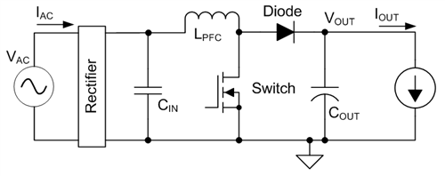
The output capacitor is the main energy storage element in a boost power factor correction (PFC) circuit (Figure 1); it is also one of the larger and more expensive components. Many factors govern its choice: the required capacitance, ambient temperature, expected service life and physical room available. In this post, I want to look at the ripple current that flows in the capacitor. The most accurate way to predict the ripple current is to do a numerical simulation, but there are some simple formulas that can give you a fairly accurate estimate of the currents, as well as some insight into how these currents vary with operating conditions.

Capacitance

As I said, the output capacitor is a relatively expensive component, so you will likely choose the minimum amount of capacitance that still will enable the design to meet its specification. All other things being equal, a smaller capacitor will have a lower cost than a larger one. Two main considerations determine how much capacitance you will need: the required holdup time and the allowable ripple voltage.

For the required holdup time, you can use Equation 1 to calculate the required capacitance:

where Pout is the power taken from the output capacitor, thu is the required holdup time, and Vinitial and Vfinal are the initial and final capacitor voltages, respectively.

If holdup time is not important, then you can size the capacitor according to the allowable voltage ripple. Equation 2 gives Cout as:

where Iout is the load current and Vripple is the peak-to-peak voltage ripple on the capacitor.

Figure 1: Typical boost PFC schematic

Capacitor current

A rearranged Equation 2 can determine the low-frequency ripple voltage on the capacitor. This ripple is sinusoidal, provided that the line current drawn by the PFC stage is sinusoidal. It will be at twice the line frequency and you can calculate the ripple voltage’s peak-to-peak amplitude with Equation 3:

The low-frequency ripple current in the capacitor is very simply related to the output current. Equation 4 gives the RMS (Root Mean Square) value of the current because most capacitors are specified in terms of RMS ripple currents. The result here agrees closely with numerical simulation results:

The ripple current also has a high-frequency component at the PFC switching frequency and its harmonics in addition to the component at twice the line frequency. You can use a slightly modified version of the formula in Erickson and Maksimovic’s “Fundamentals of Power Electronics” to calculate the RMS total capacitor ripple current. This formula ignores the effect of inductor switching-frequency ripple current and thus underestimates the current when compared to a numerical simulation. This underestimation becomes proportionally greater at high line, but because ripple currents are greatest at low line, Equation 5 is accurate to better than about 10%:

The high-frequency component of the capacitor current is then the total current minus the low-frequency current. The result that Equation 6 gives is an RMS value:

Some things to note

I looked at a single-phase CCM (Continuous Conduction Mode) PFC stage in this post, but the low-frequency ripple calculation is also valid for interleaved, CrCM (Critical Conduction Mode) and DCM (Discontinuous Conduction Mode) designs. The high-frequency ripple calculation is valid for single-phase CCM designs only, however.

Both low- and high-frequency ripple currents are not functions of the amount of capacitance. Low-frequency current is a function of the output power; it is not a function of line voltage. High-frequency ripple is greatest at low line and is a function of line, boost inductance and output power.

Check out TI’s portfolio of analog, digital and combination PFC controllers or learn the basics of power factor with the blog post, "What does a beer and power factor have in common?


What is a smart gate-drive architecture? - Part 1

$
0
0

Control, efficiency, protection … these are all terms you hear regarding new integrated circuits, but what do they really mean? While I can’t speak to all of the devices, I can talk about a new technology that Texas Instruments is introducing with its motor gate drivers. Our motor gate drivers for brushed DC, stepper and brushless DC motor applications are using a new architecture called smart gate drive. In this blog series, I’ll give a quick overview about what it is, which motor gate drivers are using it, and where you can learn more.

TI’s smart gate drive architecture is a combination of protection features and gate-drive configurability provided by the gate driver itself through two features called IDRIVE and TDRIVE. In the first installment of this two-part series, I’ll give an overview on IDRIVE. In the next installment, I’ll cover TDRIVE.

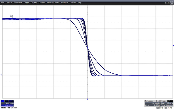
IDRIVE is the ability to dynamically adjust the gate driver’s output drive current. Getting into the specifics of how this works is outside the scope of this series, but you can refer to this application report about IDRIVE/TDRIVE to learn how gate-drive current affects the power MOSFET. In short, IDRIVE enables control of the MOSFET VDS slew rate, an important parameter in switching power designs, through a simple register write or analog voltage setting. Figure 1 shows this feature in action. The figure is a persistence scope capture of the VDS slew rate on the DRV8305-Q1EVM, ranging from 10-70mA of drive current.

Figure 1: DRV8305-Q1 IDRIVE example

MOSFET VDS slew rate is important because it is a key parameter for achieving optimal switching efficiency and minimal parasitic effects. Switching efficiency as it relates to slew rates is relatively well understood, but many of the parasitics effects are not as obvious. Two common parasitic side effects related to MOSFET VDS slew rate are switch-node ringing and electromagnetic interference (EMI).

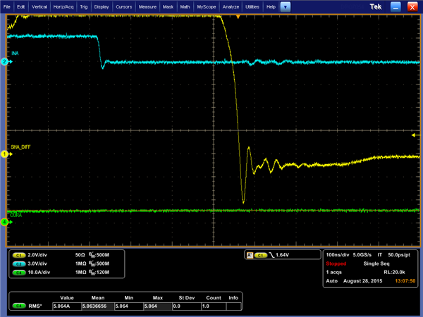
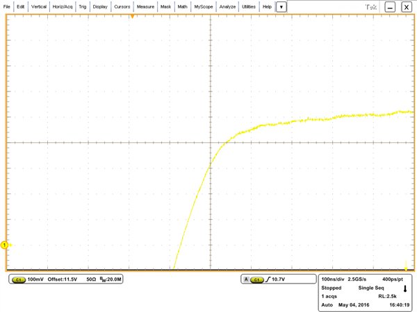
Switch-node ringing occurs due to high dV/dt (slew rates) and parasitic inductances and capacitances of the power MOSFETs and PCB layout. This ringing can cause the switch-node voltage to drop below ground or rise above the supply, often violating specifications of the gate driver or power MOSFETs and thus leading to catastrophic breakdowns. Figure 2 shows an example of switch-node ringing (in yellow) causing a large negative spike and violating the gate driver’s absolute maximum rating.

Figure 2: Switch-node ringing example

While you can tackle switch-node ringing with external components such as Schottky diodes or resistor/capacitor (RC) snubbers, often the best method is to adjust the VDS slew rate and reduce the dV/dt component of the equation. IDRIVE gives you the ability to quickly make this decision in the design phase and ensure that it remains constant over the system’s lifetime.

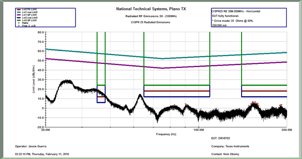
Another subtle problem faced in switching power designs is EMI, often attributed to switch-node ringing but with a different failure mode. Instead of violating an absolute maximum rating, the switch-node ringing introduces high-frequency components that radiate to nearby components and systems. This can show up in compliance testing when a product exceeds acceptable interference levels.

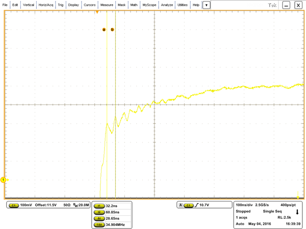
Figure 3 shows another example of switch-node ringing, but this time the high-frequency oscillation and its harmonics are translating into higher RF emission levels, as shown in Figure 4.

Figure 3: Switch-node ringing EMI example

Figure 4: EMI scan example

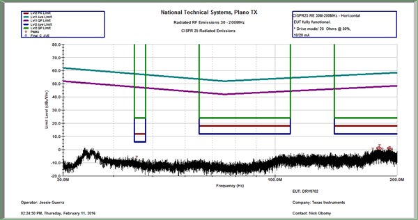
Adjusting IDRIVE enables modification of the MOSFET slew-rate and removes the high-frequency ringing, as shown in Figure 5. Figure 6 shows the corresponding RF scan with largely reduced RF emission levels.

Figure 5: Switch-node ringing removed

Figure 6: EMI scan ringing removed example


With these topics in mind, Texas Instruments has just released the DRV8305-Q1 brushless DC motor gate driver with smart gate drive, designed specifically for automotive applications such as pumps, valves, fans and more. Automotive applications are the perfect fit for a smarter gate driver due to high reliability and stringent electromagnetic compliance (EMC) requirements. To learn more, check out the DRV8305-Q1 data sheet.

In my next post, I’ll cover TDRIVE, the other half of TI’s smart gate drive architecture, and how it makes motor systems more reliable and efficient.

Additional resources

2016: The wireless audio market is finally converging!

$
0
0

The past year was a good year for wireless audio. We see growing quantities and even higher forecasts for the next five years. Although everybody is happy about the growth, one still hears a lot of parties in the industry complaining about the diversity of solutions, and the very different solutions per market segment.

We are now noticing that this solution diversity is changing. Below are several trends we’ve noticed recently:

  • The high-end audio segment is finally, after years of hesitation,  taking streaming audio and wireless audio on board
  • The CEDIA segment has adopted wireless, next to the wired home
  • The mainstream consumer market is starting to go after Wi-Fi®-enabled speakers and we expect that headphones will follow
  • Google Cast™ seems to be establishing itself as the de-facto open standard
  • The battle field of music services is seeing a concentration and a shake-out – may the best streaming service win!

StreamUnlimited has created a flexible software stack that caters flexibly for all trends mentioned above. As a special feature, StreamUnlimited has worked with TI on a special enhancement, where in combination with Sitara and WiLink8 it is possible to synchronize two loudspeakers below two microseconds, giving ultra-precise in-room wireless synchronization for left/right speakers providing a high-quality audio experience.

This can be achieved with:

TI’s Sitara processor family

Furthermore StreamSDK now has:

  • Integrated Google Cast
  • Integrated Dirac, for room correction
  • Integrated music services like Tidal, Airable and a variety of other well-known integrated music services
  • Support of WiSA wireless multi-channel technology from Summit

Every software block can be activated or deactivated, creating a wide range of products with the same software stack: from a simple Google Cast speaker to a can-do-everything streaming device for multi-channel multi-room. Depending on the functionality one can choose a cheaper or a higher-performing hardware.

A  Wi-Fi audio cape for BeagleBone Black is available as a TI Design reference design for fast prototyping (also usable for ioT applications)

Here are additional resources for more information about wireless audio solutions:

Quantifying the value of wide VIN

$
0
0

When designing a power supply, one of the challenges designers often face is dealing with voltage transients. It is important to protect circuitry from voltage spikes greater than the rated input voltage (VIN) of the integrated circuit (IC). When dealing with voltage transients, designers have a choice between using a DC/DC converter on the front end of the system with a wide-enough input voltage range to cover any transients, or a lower VIN DC/DC converter with additional clamping circuitry to provide transient protection.

At first glance, it may appear that choosing the first solution, a DC/DC converter with a wide VIN input rating of 36V or 60V, is more expensive because the 1ku price is higher than a converter with a lower voltage input rating. However, the extra voltage-clamp circuitry needed for the transient protection of a lower VIN converter can add 10 to 12 external components that will increase the bill-of-materials (BOM) count and cost, as well as solution size. In this post, I will compare the solution size and cost of the SIMPLE SWITCHER® LM43603 36 VIN, 3A buck converter against a comparable 17 VIN, 3A converter solution with additional clamping circuitry used to absorb the surge voltage. 

The schematic in Figure 1 is an example of a discrete solution used to clamp the input voltage when the IC’s voltage rating is lower than the maximum input spike. This solution uses the LMV431 shunt regulator and a PNP transistor as a control circuit. The P-channel field-effect transistor (PFET) carries the pass-through current and has an increased voltage drop as the VIN surges and thus takes the increased power loss and protects the DC/DC converter. More detail on this technique can be found in the application note “Over Voltage Protection Circuit for Automotive Load Dump.”

As seen in Figure 1, this input clamping control circuitry and PFET adds 13 extra external components to the solution. As Figure 2 shows, based on 1ku quantities published online, these 13 external components would add $1.19 to the total cost. The solution cost of a 17 VIN, 3A converter may be around $1.62, using 1ku-quantity pricing of $0.96 and including the cost of external components like the inductor, capacitors and resistors. This brings the total solution cost of using a 17 VIN buck converter plus clamping circuitry to approximately $1.62 + $1.19 = $2.81. Additionally, the control circuitry and PFET add approximately 210 mm2 to the solution size of the lower VIN solution. A 17 VIN, 3A converter may be around 100 mm2, which makes the total solution size 100 mm2+250 mm2 = 350 mm2.

Figure 2: Control circuit cost breakdown

Another option is to use a DC/DC converter with a wider input-voltage range to cover the maximum VIN spike like the SIMPLE SWITCHER® LM43603 36 VIN, 3A synchronous buck converter. Using a wide-VIN device like the LM43603 enables designers to eliminate the additional clamping circuitry which saves time, cost and board space. The total solution cost of the LM43603 is approximately $2.51 using the published 1ku quantity price of $1.85 and including the cost of external components like the inductor, resistors and capacitors. This means that using the wider VIN LM43063 saves $0.30 or approximately 12%: $2.51 vs. $2.81. The benefits increase when you look at solution size. The total solution size of the LM43603 is approximately 250 mm2 which is about 24% or 60 mm2 smaller than the previous solution.

Another benefit to a wide VIN solution like the LM43603 is increased reliability. As I talked about in more detail in an earlier post, adding additional external components introduces additional risk into the system. The most reliable solution is the simplest solution with the fewest number of external components, because it reduces the risk of one component malfunctioning. Increasing reliability is very important particularly in the harsh conditions of some automotive and industrial applications. Plus, designing the additional clamping control circuitry adds significant work to the design cycle. Using the control circuitry and PFET means that you must select 12 more external components and run additional testing and simulations to ensure that it works. Why put in that effort when you can get a regulator with a wider VIN range with lower system costs and higher reliability?

Of course, pricing and solution size can vary widely based on volumes and contracts between vendors and suppliers, as well as design layouts. The size and cost percentage saved with a wide VIN solution will likewise vary. However, I hope this analysis shows that despite the higher upfront 1ku price, a wide VIN solution like the LM43603 can provide savings in solution cost, board space and design time when dealing with input-voltage transients.

Get more information on TI’s wide VIN DC/DC power solutions.

Why should you care about over-current protection in your system?

$
0
0

Everywhere we go, new electronic devices are popping up to make life easier or more efficient. As we come to rely on these devices, it becomes imperative that they just “work” – regardless of the operating environment. Whether it is the always-on smartphone, our ever-more-electronic vehicles, the self-checkout kiosks at our favorite restaurant or a large factory automation system that we do not directly interact with but have just come to accept as part of life – we just expect things to work.

Figure 1: Examples of the many electronic devices that we have become part of our everyday life

One major way to prevent downtime in modern electronic systems is to detect, react to and fix potentially damaging conditions as rapidly as possible. However, two macrotrends make this a larger challenge. The first is the desire for more performance, despite the fact that today’s electronics have processing power that’s orders of magnitude greater than their predecessors just since the early part of the millennium. The second is packing all of this additional performance into shrinking form factors.

System thermal management has become one of the most prevalent methods for implementing damage detection and prevention. Historically, designers monitored temperature to protect systems; as the temperature rose, a fan could turn on to reduce the ambient temperature. However, with the trend toward smaller form factors, in many cases there is just not room to implement a space-consuming solution like a fan.

The demand for greater performance can cause a significant rise in temperature in a short period of time. In most cases this temperature increase results in a power consumption increase. Rather than measuring a lagging indicator (temperature), many designers choose to measure a leading indicator, current (or power, which is the voltage multiplied by the current). Overcurrent protection enables designers to manage system thermal performance more efficiently and anticipate problems proactively vs. reacting to potential issues.

There are many reasons to monitor for overcurrent conditions:

  • Long-term system reliability.
  • System/user safety.
  • System efficiency.
  • Fault protection.

If you would like to learn more about the challenges of system thermal management and how Texas Instruments is enabling more accurate and precise overcurrent detection to help solve this challenge, please download my white paper, “Overcurrent protection enables more efficient and reliable systems with longer lifecycles”  or check out the Texas Instruments portfolio of current sense amplifiers.

Additional Resources:

Pump up the volume by streaming audio with a Wi-Fi® mesh network

$
0
0

Wireless audio appeared a few years ago, and has been progressing and improving since then. In recent years, manufacturers have turned to Wi-Fi® as a method to transfer audio data which makes a lot of sense for the following reasons:

  • Wi-Fi throughput is very high compared to other wireless standards.
  • It has a longer range than other connectivity technologies commonly associated with audio streaming.
  • It has features that allow for optimal synchronization of audio.

Sounds perfect right?

Well, like any technology implementation there are challenges to overcome. Here, the problem starts with infrastructure. When using a standard star Wi-Fi topology, all speakers must be connected to a single central entity to play music, which limits the user in the placement of home speakers, for example.

The solution? IEEE 802.11s: Or in a less formal name – mesh. With a mesh topology, the possibilities grow larger and limitations dwindle. Infrastructure? No problem. With mesh, every node is connected to each other and everything is efficiently distributed across the network with no central entity. In essence, mesh allows devices with the same configured profile to connect to each other on MAC level. For example, two speakers that are not in range of each other can still be connected through other speakers between them that are in range, turning each speaker into a range extender, among other things.

Mesh packs a lot of features:

  • Self-healing: Replaces paths when a link crashes, so that you never skip a beat!
  • Self-forming: Automatic connection between all configured nodes.
  • Path selection algorithm: The network automatically chooses the best path for packets for extra speed and shorter latency.
  • Range extension: Extend the coverage of Wi-Fi using mesh nodes.
  • Network offload: Mesh links are direct, and traffic does not always have to flow through the home AP.
  • Improved network capacity: In some cases, an improvement in network capacity is achieved due to the distributed nature of a mesh system.

But the most important feature is this: 802.11s is a standard and we at TI have embraced it and now provide mesh capabilities on all of our WiLink™ 8 Wi-Fi + Bluetooth®modules.

Our WiLink 8 Wi-Fi mesh solutions offer even more features than standard implementations:

  • Time synchronization: Enables incredible audio synchronization between all speakers in a zone.
  • Enhanced path selection algorithm: TI’s Wi-Fi mesh brings path selection to the product level, improving throughput, latency and decision making for systems

Imagine this: You go to the beach with your friends and each person brings their own wireless speaker. They all connect, sync flawlessly and play your music – together.

Want to get more oomph out of your sound system? Get another speaker and place it in the range of another and you are done! Have a set of speakers in your basement but no network coverage? Use mesh to extend your network’s range to turn your basement into a dance hall!

A Wi-Fi mesh system will allow a seamless connection that can cover your entire home, even when no central entity is present. Just place that speakers anywhere you want and get that music going!

The solutions and possibilities that a mesh system brings to wireless audio are endless, and with our WiLink 8 combo-connectivity modules you can start making your own today!

So, shall we Tango?

Additional resources:

  • Learn more about WiLink 8 module audio solutions
  • Download our white paper about Wi-Fi mesh capabilities
  • Read about our advanced audio synchronization capabilities
  • Watch our Wi-Fi mesh networks audio demo video below

(Please visit the site to view this video)


DIY with TI: TIer crafts disco rollerblades, high-tech night light

$
0
0

At TI, we celebrate the makers and hobbyists who enjoy creating and innovating on their own time. In our ongoing DIY with TI series, we share their incredible Do It Yourself inventions using TI technology.

TIer and DIY enthusiast Max Groenig has created a pair of LED rollerblades to light up the night.

The idea came after Max attended Munich Blade Night, in which the streets are closed to traffic so thousands of inline skaters, quad skaters and skateboarders can take to the streets. During the event, Max noticed skaters holding light strips and had the idea to add lights to the skates themselves.

Max worked with a colleague in our Freising office to create the lighting system. The LEDs change color and flash rhythmically when skaters travel at different speeds to give the impression of disco lights. In addition, the lights flash red if the skater falls. Up to 16 LEDs can be fitted to the base of the skate, with a printed circuit board for every four LEDs. The system uses a MSP microcontroller, an acceleration sensor and LED driver.

The electrical gene

You could say that electronics are in Max’s blood.

His electrician father introduced him to the delights of electronic design at the age of six, and Max went on to study electronics engineering at the University of Bremen. After securing an internship with our office in Freising, he joined us full time as a software engineer.

An avid DIYer, Max also has come up with a solution to things that go bump in the night.

TI AvatarIt’s a familiar scenario: you get up in the middle of the night and stumble on something in the dark. Max’s idea was simple: place lighting under the bed that slowly illuminates when you step out of bed and fades when you return.

Looking for a low-cost but effective solution, Max used an MSP430™ microcontroller (MCU) LaunchPad™ development kit with a debugger tool as the development platform. He attached the device to a computer via USB and wrote the software code to control the system. Other main components included a printedcircuit board – the MSP-EXP430FR5739 Experimenter Board– an infrared motion sensor and a 5-meter length of LED lights.

Max prototyped the system over the course of few evenings and weekends, tuning the printed circuit board to handle the correct current and voltage, and the LaunchPad to mix red, blue and green frequencies to create the right shade of white light.

The lighting is triggered by the infrared sensor, which detects a temperature change when feet are moving around the bed at a radius of up to three meters. Since it is a passive sensor, it only requires power when activated.

One of the biggest challenges was lighting the room in a way that wouldn’t be too bright or sudden for anyone still sleeping.

“I didn’t want the light to disrupt people who may be sleeping in the room,” Max said.

The human eye doesn’t detect an increase in light intensity in a linear way, so Max incorporated a formula that ensured the increase in light received by the eye would appear smooth.

Another idea Max is working on is a hybrid-powered skateboard with an on-board engine and an energy-recovery system that harvests braking energy and redeploys it to provide additional power. Max noted that although similar technology is available to buy, it’s more satisfying, and often much cheaper, to make such systems yourself.

Here’s to that maker spirit, Max.

Designing an IoT modular light

$
0
0

LED lighting applications have revolutionized the world – not only in general lighting but in anything that uses illumination, like LED displays, portable illumination systems, medical instruments and even scientific equipment.

In the winter of 2015, element14, Texas Instruments and Würth Elektronik invited a select group of designers to a “road test plus” – we were told to design something around the TI TPS92512 buck LED driver using evaluation boards and parts. My application was accepted to participate and I went on to implement a simple yet practical Internet of Things (IoT)-based lighting solution that won the challenge in the end.

In this two-part series, I’ll summarize my experience with and thought process behind the challenge, highlighting key milestones in the implementation process. What initially started as a prototype project which could be used for a multitude of things finally evolved into a multipurpose IoT light that I used in my newborn’s room.

The proposal

 My basic idea was to create an IoT lighting-based project, with the ability to connect to the Internet and accept values for color and brightness. The project uses the TPS92512 as the hero of the design, with a TI SimpleLink™ Wi-Fi® CC3200 wireless microcontroller (MCU) LaunchPad™ development kit to enable a Wi-Fi-based connection to the Internet. The commands come in via the Message Queue Telemetry Transport (MQTT) protocol over the Internet, and the TPS92512 controls LED brightness.

 My single-channel LED light prototype is controllable through a website that uses a client-side JavaScript® MQTT library to send commands from a web browser to the TI CC3200 wireless MCU LaunchPad kit via the iot.eclipse.org MQTT broker. I wrote the firmware for the CC3200 device using Energia, which is the Arduino equivalent for TI LaunchPad kits and works even better. Figure 1 shows the initial block diagram.

Figure 1: Proposed system block diagram

Driving LEDs and the TPS92512

Just like any other component, a correctly driven LED will improve its lifespan as well as its efficiency. You can also control the illumination characteristics by varying the drive of the device. The LED is essentially a diode, and the forward-bias characteristics (especially Vf) vary slightly from unit to unit as a consequence of the manufacturing process.

Examining the data sheet for Würth Elektronik’s indium gallium nitride (InGaN)-based ceramic-chip LEDs, you can see that the LED’s forward current increases sharply with the forward voltage and is almost linear beyond the knee voltage. The luminous flux also varies as a function of the forward current up to a limiting value. Thus, it would be more beneficial to control the current through the LED when driving it, using a current-control scheme to obtain better results.

Figure 2 from the mentioned datasheet shows this trend graphically where we see forward current as a function of forward voltage and luminous flux as a function of the forward current.

Figure 2: Forward current as a function of applied voltage and its effect on luminous flux output

There are a number of ways to arrange a constant-current source, including the classic LM317 circuit, as shown in Figure 3. The problem is the maximum current you can drive. You can cascade more than one LM317 in parallel, but that is not very cost-effective.

 Figure 3: Circuit diagram for an LM317 based constant current source

Alternatively, you can use an operational amplifier/comparator with a voltage reference and then use a transistor or MOSFET at the output stage to perform the regulation manually as shown in figure 4. This works better and is how I usually design power-supply circuits. The major issue with this approach, however, is the amount of board space used, as well as bill-of-materials cost. You end up assembling a large circuit – which is OK when you need to handle a lot of current in the range of tens of amps – but for LEDs this is overkill.

 Figure 4: A high side current control circuit using an op-amp

So you need MOSFETs for efficiency but don’t want to make your own module. The solution is a dedicated driver chip like the TPS92512, which has the MOSFET as a switch as well as thermal shutdown, and internal oscillator and pulse-width modulator (PWM) logics for control. Other solutions out there require an external MOSFET switch as well as some miscellaneous passives. The TPS92512 is simpler to use; Figure 5 shows its functional block diagram.

Figure 5: Functional block diagram of the TPS92512

The TPS92512 is capable of driving up to 2.5A; the standard version can operate with a VIN up to 48V. A standard microcontroller with a Pulse Width Modulation (PWM)signal can drive the TPS92512 to vary the output current and therefore LED brightness.

In part 2 of this series, I’ll show you how I built the prototype.

Additional resources


Designing high-performance, cost-sensitive transimpedance op-amp circuits

$
0
0

This post is co-authored by Raphael Puzio.

Photodiode-based light sensing is a common application of operational amplifiers (op amps) used in medical equipment, industrial automation, robotics, point-of-sale machines, drones, smoke detectors and building automation equipment.  This blog demonstrates how to build a cost-sensitive, accurate photodiode circuit.

A photodiode sensor produces a current proportional to the light level presented to it. Depending on the application, the photodiode is operated in either a photovoltaic or photoconductive mode; each has its own merits, which Bruce Trump discussed in detail in this post from his blog, The Signal.

Most applications operate the photodiode in photoconductive mode, with an op amp in a transimpedance configuration to amplify the current. In photoconductive mode, the photodiode is held at a zero-volt (Figure 1a) or reverse voltage bias (Figure 1b), preventing it from forward biasing.

Figure 1: Photodiode in photoconductive mode with zero-volt bias (a); or reverse-voltage bias (b)

Equation 1 calculates the direct current (DC) transfer function for the circuits shown in Figure 1 (note that the photodiode current (iD) is flowing away from the op-amp inverting node):

The three-step process outlined in John Caldwell’s series on transimpedance amplifiers (see part 3, “What op amp bandwidth do I need?”) determines the minimum required op-amp gain bandwidth for transimpedance configurations. The minimum bandwidth is based on the required transimpedance gain and signal bandwidth, along with the total capacitance presented to the inverting node of the op amp. The diode capacitance often dominates the inverting-node capacitance, but don’t forget to include the effects of the op-amp input capacitance. We summarized the three steps explained in John’s posts here for quick reference.

1. Choose the maximum feedback capacitance (CF) based on the feedback resistor (RF) and the signal -3dB bandwidth (fP) (Equation 2):

 2. Calculate the total capacitance (CIN) at the inverting input of the amplifier. For the circuits shown in Figure 1, this is equal to Equation 3:

where CJ is the diode junction capacitance, CD is the op-amp differential input capacitance and CCM2 is the op-amp inverting input common-mode input capacitance.

3. Calculate the minimum required op-amp gain bandwidth product (fGBW) (Equation 4):

By following these three simple steps, you can avoid many of the stability and performance issues commonly associated with transimpedance amplifier circuits by selecting an amplifier with sufficient bandwidth to perform the required transimpedance gain at the desired signal bandwidth.

Along with meeting bandwidth requirements, the op amp must also meet the system’s DC accuracy requirements. The most important DC specification in many transimpedance applications is the input bias current (iB) of the op amp. iB will directly sum or subtract with the input signal current, which can cause large errors depending on the magnitude of iB compared to the signal current.

The example shown in Figure 2 uses a 5MΩ resistor to apply a 5MV/A gain to a 100nA full-scale input current. With the input bias current set to 0A, the full-scale output voltage is 500mV – which is expected based on the transfer function in Equation 1. The circuit on the right in Figure 2 displays the effects of the same circuit with an op amp iB of 10nA. In this case, the output voltage is 450mV, which shows that the 10nA input bias current caused a 50mV (or 10%) error from the ideal 500mV output signal.

Figure 2: Input bias current effects in transimpedance amplifier circuits

Equation 5 calculates the percentage error of the full-scale range (%FSR) based on the full-scale input current (iIN_FS) and the op amp’s iB:

The TLV600x devices are a new family of high-performance general-purpose amplifiers for a wide variety of cost-conscious transimpedance applications, such as consumer drones, POS machines, smoke detectors and building automation equipment. The key features that make the TLV600x great for transimpedance applications is the wide bandwidth of 1MHz, low typical input bias currents of 1pA and a low input capacitance of 6pF total. Other beneficial features are a low quiescent current of 100µA maximum, rail-to-rail input and output swings, and low current and voltage noise densities of 5fA/√Hz and 28nV/√Hz, respectively.

Table 1 lists different transimpedance gain and bandwidth combinations for the TLV600x based on Equations 1 through 4. Be sure to keep the total input capacitance below the maximum input capacitance (CIN­_MAX) to avoid stability issues.

Note: fGBW is 1MHz, CD is 1pF and CCM is 5pF for the TLV600x.

Table 1: Quick design calculator for TLV600x transimpedance applications

Figure 3 shows the simulated step-response results for a 1MV/A gain and 50kHz bandwidth with the maximum 54pF of input capacitance from the photodiode. The output overshoot and ringing are minimal, indicating a stable design.

Figure 3: TLV6000 step-response results; gain = 1MV/A, bandwidth = 50kHz

Many applications use op amps in the transimpedance configuration to amplify low-level currents. Designing the transimpedance circuit can be simplified to a few easy steps. First, follow the three steps from John’s blog posts to select the required op-amp bandwidth. Then sort the remaining results to find a device with an iB specification that meets the system’s DC requirements.

Do you have questions about transimpedance op-amp designs? Log in and leave a comment below letting us know your experience with transimpedance configurations or any questions you have.

Additional resources

Shrink your industrial footprint with new 60V FemtoFETs

$
0
0

In Shenzhen, China, recently I met with a designer for an infotainment systems manufacturer. “Do you happen to use any 60V load switches in your design?” I asked. He affirmed, telling me he incorporated about 10 30V-60V small-outline transistor (SOT)-23s on his board, generally around 100mΩ RDS(ON). “And on these boards, are you space-constrained?,” I asked. Turns out that he was, so I showed him information on TI’s new CSD18541F5 60V FemtoFET MOSFET, coming in at just under 60mΩ with a 1.5mm-by-0.8mm (1.2mm2) footprint (see Figure 1), that was designed specifically for space-constrained applications such as infotainment systems. 

Figure 1: CSD18541F5 land grid array (LGA) package

That’s roughly one-sixth the size of an SOT-23 (6.75mm2) package for those of you keeping track at home (see Figure 2). It also represents an RDS(ON) multiplied by footprint size figure of merit that is 75% smaller than traditional MOSFETs.

Figure 2: Traditional SOT-23 package next to the CSD18541F5 LGA package

Doing some quick math with this engineer, we determined that with 10 devices per board, he’d be saving roughly 55mm2– not an insignificant amount for a device generally considered an afterthought by most engineers. And what about pad pitch?  Fortunately, the tiny LGA package was designed to accommodate industrial customers as well, for whom the consensus seems to be that a 0.5mm pitch is the preferred minimum distance between pads.

Today, almost everyone I visit in the industrial market, whether they’re manufacturing power supplies, battery protection or power tools, has had some interest in either a smaller- or higher-performing load switch (or both).

So if your industrial design features more than a few SOT-23s or larger load switches, consider switching to our new CSD18541F5 MOSFETs. Trust me, your PCB footprint will thank you later.

Additional resources

Collaboration fuels innovation

$
0
0
It’s hard to believe it has been more than a year since I published the inaugural post for this blog. Since that introductory post in April 2015 , several exciting innovations have continued to unfold, building on the amazing legacy of DLP®...(read more)

Advantages of wide band gap materials in power electronics – part 2

$
0
0

In the first installment of this series, I explored how gallium nitride (GaN) enables operation at higher frequencies and how that allows for smaller component selection. This ultimately shrinks product size while maintaining the same power level: hence the power density increases.

Smaller products: the increasing power density

As the power density of a power supply increases due to the shrinking of its components, what happens to the heat generated?

Heat management can become challenging as the power-loss density increases. For a given aspect ratio, the area available for heat exchange reduces as the volume reduces, which leads to a higher surface temperature.

Efficiency improvements become necessary to enable shrinking in the size of power systems. From a loss point of view, a 90% efficient system has twice as much power loss as a 95% efficient system: every percentage point counts.

Another driving factor pushing for higher efficiencies are the governing regulations and standards for power supplies, which are becoming increasingly stringent. More marketing-related green certifications also require increasingly higher standards.

Improving efficiency

In an application using GaN transistors, you can take two main paths to improve a particular application.

The first is to maintain operational frequency close to an equivalent silicon-based system, since the GaN-based FET has less loss.

The second is to shrink the system by increasing the frequency, in which case transition or switching losses become a dominant element again.

In the second case, where the power density increases, there is a need to further improve efficiency.

The best way to reduce switching losses is to adopt a resonant or quasi-resonant scheme. The same basic concept applies: switch the transistors with either zero current or zero voltage across them (or close to zero). A number of such topologies already exist with silicon solutions that you can extend to GaN.

The advantage of using GaN is that the switching frequencies and transition speeds are high enough that you can use the parasitics from passive components as part of the design to tune the resonance. Smaller parasitics will also result in lower circulating currents and enable shorter dead times. This inherently simplifies the design, reducing cost, weight and all of the extra losses associated with extra components.

You can reduce conduction losses by taking advantage of the high frequency to reduce current ripple (lower current peaks generate lower conduction losses). A good example in AC/DC conversion is an active-switch power factor correction (PFC) circuit, where the charging current is sinusoidal rather than pulsed, thus reducing peak-current conduction losses. Similarly, the effectiveness of active switches can be maximized by using very fast controllers, so to present as low impedance through the power stage, thus improving efficiency.

You can further improve the reduction in driving losses coming from the lowered activation voltage and lower gate charge (Qg) with resonant gate-driving techniques.

Conclusion

Size reduction and improved power-conversion efficiency are the two major visible advantages of using GaN in power systems.

Depending on the system, increasing the frequency beyond a certain limit may not be advantageous for size reduction, as the system’s non-power-related components might not be able to shrink accordingly (power connectors, motors). In those systems, the reason to push for a higher frequency is to push the electromagnetic interference (EMI) beyond the scope of standards.

GaN is the greatest major paradigm shift in power supplies in decades, and with the extremely high switching speeds achieved (100/ns), a GaN switch is the closest thing to an ideal switch available.

GaN opens up the possibility to revisit classic power supplies, improving performance, efficiency, cost and size. More importantly, it enables designers to explore and invent new topologies that were not conceivable with silicon.

Get to know TI GaN solutions and begin your design. 

Out of office: Matchpoint! Pro tennis player finds new game

$
0
0

The game of tennis taught TIer Izak Van der Merwe a lot about life – including perseverance, humility, discipline to train hard, and taking ownership of your game, he said.

These qualities have served him well as he has transitioned from being a world-ranked professional tennis player to a credit manager in our finance department.

“Naturally, I don’t consider myself a competitive person. Tennis drove me to be competitive,” said Izak, a 6-foot-5, 32-year-old who has represented his native South Africa in the Davis Cup competition and has competed three times at Wimbledon. “If you’re good at something, that competitive spirit works alongside your passion. I don’t want to be competitive in my-day-to-day life, but in tennis you have no choice.”

Izak said he ran his tennis career like a small business.

“You only get paid if you win enough matches. You have to perform to be able to put some money in the bank,” he said. “It definitely teaches you the discipline to work hard at your trade, build the skills you need and persevere in difficult times.”

(Please visit the site to view this video)

Izak first picked up a tennis racquet at age 5 when his parents started dragging him and his two brothers to tennis clubs on weekends.

“When I was 5 or 6, they apparently saw some potential in me,” he said. “Playing Wimbledon was a boyhood dream for me.”

Izak quickly blossomed as a player and started competing internationally at age 14. He turned pro at 21, winning numerous titles and ranking 113th in singles and 94th in doubles in 2011 in the ATP World Tour. Watch a short video of Izak here.

One of his most memorable career highlights was playing in the finals of the ATP Challenger tournament in Brazil at age 26. The crowd was cheering for the local favorite in the singles finals – which can unnerve the best of players. “Besides my coach, I think the whole crowd cheered for my opponent, their countryman and local favorite.

“I used the crowd and the environment as the driving force to buckle down and play hard instead of letting it get under my skin,” he said. “The only thing you can do is ‘play the crowd quiet’ and shut them down.”

Izak succeeded, winning the match in just two swift sets and claiming his first ATP Challenger title.

Another high point was representing South Africa in 13 Davis Cup ties, competing against countries such as Germany, Canada and India among others. Izak has a very loyal public fan base back home, so he enjoyed having the support on his side of the net during those matches.

“It was nice knowing a lot of people were watching and supporting me. I felt like the whole crowd was behind me – which can get under the skin of the other player,” he said, smiling.

Izak collected more than $430,000 in prize winnings during his tennis career.

As with many competitive sports, injuries took their toll on Izak. First, he had to have surgery on his foot because of a chronic Achilles heel injury. He thought that was the end of his career, but he underwent physical rehabilitation and continued playing. Then he began having knee issues.

“I had been struggling with injuries for a couple of years, so it was not a rush decision,” he said. “But I still wish I could have played for a little longer. It was a great passion in my life.”

Izak moved to Dallas to train in 2013 and played his last professional tournament in March 2014. That same year, he decided to go back to school at the University of Texas at Dallas (UTD). He entered an accelerated program and earned his MBA in a year and 4 months.

“I wanted to go back to school and work for a great company because I always wanted to learn new skills,” he said. “When the opportunity came to work for TI, I said, ‘I’m going to take it.’” 

Izak was recruited late last year through a Finance, Accounting & Operations rotation program. He started his new job in January as a credit manager in our worldwide accounts receivables business in Dallas, where he works with customers who buy our Education Technology and semiconductor chips.

It’s a very different game from tennis.

“It’s definitely a big change from the tennis tour. In my tennis career, I always felt like I was prepared for the match – confident in my abilities,” he said. “In work, I am always learning, so I have to build that confidence step by step. You learn to use the tools you have to solve problems.”

IzakThe biggest difference in his two careers is working on a computer instead of a tennis court, he said. Tennis was both mentally and physically taxing, requiring five to six hours a day of training. At the peak of his career, Izak was competing in 30 tournaments per year all over the world. For his training, he split his time between Cape Town, South Africa, and Virginia Beach, Va., because his coaches were based in these locations.

“The professional tennis tour doesn’t have boundaries, and traveling to more than 30 countries during my career was a great experience,” he said.

Izak has been immersed in his new job at TI for the past few months, but also enjoys mountain biking and golfing in his spare time.

“I like golf because it’s laid-back,” he said. “It’s a very different sport from tennis.”

Now that summer is here, Izak is starting to play tennis again for leisure. He hopes to play in a few tournaments in the Dallas area and has resumed coaching some promising young tennis players who are home from college.

“It’s fun to work with some high-level tennis players. You feel like you were in their shoes just a few years ago, so you know what they are going through,” he said.

As for the lessons he learned playing tennis, they have served Izak well, said Bert Leatch, credit manager. Izak is the first employee he has had on his team whohas made the transition from professional sports to corporate America.

“You’re not going to find anybody with a stronger work ethic,” Bert said. “Izak will put in whatever is needed to learn the job.”

Izak has been a great fit, said Jori Psencik, a university recruiting manager who helped hire him.

“Being a professional athlete shows passion, drive and competitiveness, all of which make him a good candidate for us,” Jori said. “He had to manage his brand, travel internationally, and have the drive to say, ‘If this isn’t going to work out, I’ll come up with something else.’

“He went out and created a new career path for himself and made things happen.”

Viewing all 4543 articles
Browse latest View live


<script src="https://jsc.adskeeper.com/r/s/rssing.com.1596347.js" async> </script>