Quantcast
Channel: TI E2E support forums
Viewing all 4543 articles
Browse latest View live

Make your smart home better connected with a Wi-Fi mesh network

$
0
0

A few years back the smart home used to be targeted only to the top echelon. It’s now 2016 and we can see smart home solutions becoming much more affordable and a normal part of daily life for the average household. Smart surveillance cameras, wireless speakers, smart doors, watering systems and so much more can all communicate, create local networks and be controlled and accessed from practically anywhere.

 When it comes to wireless connectivity what we have seen lately mainly corresponds to:

  • Faster data transfer rates
  • Security, security and then some more security
  • Lower power consumption – longer battery life
  • Smaller footprint – smaller and more affordable products

All of these have been making the Internet of Things (IoT) dream come true, however at least one major piece of the puzzle is still missing and here is where mesh fits in.

Several technologies have been leading the wireless market in the last decade or so, each one with its own edge for the IoT. But when we look for a solution that combines the most advantages for home automation, we see a lot of designers picking Wi-Fi® because it has:

  • Longer wireless range than other commonly used home automation connectivity technology options
  • Built in IP support
  • Competitive price range
  • Existing products and infrastructure already installed in the market

Wi-Fi® topology is such that an ad-hoc connection can be created via peer to peer (P2P) connections. Unfortunately, in order to create an ad-hoc network that will best suit the IoT concept, P2P is not the right way to go. It misses too many elements to create a network that will fully utilize the potential of the IoT. For that reason, Wi-Fi mesh topology, 802.11s, was introduced a couple of years ago to bridge the gap but only a few companies chose to support this type of Wi-Fi network.

Mesh brings to the table specific functions that help complete the home automation connectivity picture:

  • Any device can directly connect to any device
  • It breaks any pre-defined topology restrictions we had prior to mesh
  • It extends range from the access point and coverage becomes better on-the-fly with mesh

Texas Instruments now has mesh support with our WiLink™ 8 module which enables an almost infinite amount of new and exciting ways to develop home automation applications.  A few examples are:

  • Speakers that can create networks on-the-fly and work together to create home theater and surround sound systems
  • A water sprinkler mesh system that backs up each sprinkler in case one is not functional while also informing the user of the malfunction
  • A light bulb mesh network that knows which light bulbs are not working/connected and responds to a ‘switch on’ request by lighting the closest working light bulb
  • A home automation control panel (gateway) to monitor and control the smart home

With a mesh network, the sky is the limit when it comes to home automation and the only boundaries are the ones set by your imagination. So tell us, what is your dream smart home application?  

Additional resources:


Air quality monitors and smoke detectors put on a new face

$
0
0

Air quality monitors are not new. In fact, we all have one built right in the middle of our faces. Unfortunately, our noses are sometimes unreliable when they fail to detect odorless noxious gases or we’re fast asleep while a fire smolders somewhere close by.

Microcontroller(MCU)-based air quality monitors and smoke detectors have been around for some time too, but now a new generation of low-power, highly integrated, high-performance MCUs are teaming up with super-sensitive sensors to detect the faintest whiff of an unwanted gas or smoke particles in homes, offices, factories and just about anywhere.

For many applications like smoke detectors, these new MCUs are practically a detector-on-a-chip, minus the optics chamber. For other applications that require connection to a specialized sensor to detect a certain gas like carbon monoxide, for example, the high level of integration found in these MCUs makes them an extremely cost-effective solution.

Many MCUs have integrated memory resources, but few feature a unified monolithic memory block that avoids the constraints imposed by ‘RAM and Flash’ architectures. Basing the memory architecture on FRAM (ferroelectric random access memory) gives developers much more flexibility and configurability, simplifying how they might scale applications onto this platform.

For example, instead of having a surplus of Flash memory and not enough RAM, the system designer can configure memory to meet the needs of the application rather than shoehorning the application into a memory architecture dictated by the available memory blocks. Some applications might require more memory space to store extensive data logging to keep track of when the concentration of a gas exceeded certain thresholds. Such a detector might require that more of the available memory be devoted to Flash-equivalent storage and less to RAM for program storage. For other applications, the ratio might be reversed. With a unified memory architecture, the developer can simply reconfigure memory to meet the requirements of the application that’s being worked on at the time.

This on-chip memory flexibility points to another advantage; namely, greater integration and how this reduces bill of material (BOM) costs as well as circuit board space. In addition to eliminating external memory devices, some of this new generation of highly integrated MCUs also includes an external oscillator and analog front-end components such as operational amplifiers. A few of these new MCUs even include a super-sensitive transimpedance amplifier (TIA) capable of monitoring and converting a very low current signal into a voltage signal. As many as six discrete chips could be eliminated from an old design and the size of the circuit board might be reduced by as much as 75 percent. All that adds up to an extremely cost-effective new product design.

Of course, the greater integration also has an effect on the system’s reliability and power consumption. And fewer external parts will simplify assembly, reducing manufacturing costs.

Many residential, industrial and commercial air quality detectors are off the electrical grid and are powered by a small battery such as a coin cell or AA Cells.  So, low power consumption is a high priority because it will affect how often the detector’s battery must be replaced. In most use cases, the longer the battery life, the more beneficial the detector is for users. Homeowners would prefer to install a smoke detector and not have to change the battery for 10 years or more. In industrial settings, such as a production line on a factory floor, a gas monitor could conceivably be installed in a hard-to-reach or hazardous location. Not having to frequently install new batteries can improve the efficiency and throughput of the production line by reducing downtime for maintenance.

Interestingly, low power also helps non-battery powered or line connected addressable detectors to enable more modes on a single network increasing its capacity with limited power supply.

Another consideration for certain use cases would be backend communications, since many applications will call for the air quality monitors to be part of a larger factory automation or building maintenance system. Standard I/O interfaces like SPI, I2C and UART can provide connectivity directly to wired networks or to wireless technologies like Wi-Fi® or Bluetooth®.

Additional resources:

USB Type-C version 1.2 – USB embraces a broader market

$
0
0

USB Type-C changed the USB ecosystem in a major way by making both ends of the USB cable interchangeable (not just flippable). This enables USB devices such as laptops or smartphones to have different behavior depending upon what other USB device they are connected to, since the data role and power role can be exchanged independently. The USB Implementers Forum has now released version 1.2 of the USB Type-C specification. There are several key changes over version 1.1 that I’ll summarize in this post, but the biggest difference is a shift in the terminology used to describe this new USB ecosystem. You might say the USB Type-C terminology got a “do-over” with this version.

The new terminology does a better job explaining this new USB world, and is meant to clarify and emphasize that data roles and power roles are orthogonal to each other (except that the initial power role determines the initial data role). In other words, USB is fully embracing this new two-dimensional ecosystem. The following table has some key terms to know.

Figure 1 categorizes many of the possible applications and shows where they fall on this two-dimensional grid. 

Figure 1: USB Type-C version 1.2 example applications

 USB Power Delivery enables swapping or changing data roles. For example, there may be a dual-role data (DRD) system that is always a source of power but can be either DFP (host) or UFP (device). Alternatively, there may be a dual-role power (DRP) system that is a DFP (host) while sourcing power, but does not support data while sinking power. Discussing all of the possible applications is a topic for another post, but here I’m just trying to highlight the separation of data roles and power roles.

The initial power role and the initial data role are still associated, as they always have been in Type-C. The device that initializes as the source is either the DFP or not data capable; it may not initialize as a UFP. Likewise, the device that initializes as the sink is either the UFP or not data capable. In order to swap data roles after the initial connection, you must use the USB Power Delivery message DR_Swap. 

There are also two features in USB Type-C called default source and default sink. (Version 1.2 adds some clarifications about these features, which were previously referred to as try source and try sink, respectively.) The default source feature is intended for systems that primarily deliver power, but that also sink power at times such as a power bank. The power bank should be providing power unless it is connected to source-only or its battery runs out.  The default sink feature is intended for systems such as smartphones that primarily sink power, but can source power if connected to a sink-only accessory. These two features can be leveraged dynamically, meaning that depending upon the charge level of its battery or some other criterion, the system may change to a sink-only or default source. The following table summarizes the different kinds of roles for USB Type-C devices.

What else is new in USB Type-C version 1.2? Table 1 lists several other changes.

The max source VBUS capacitance change is worth discussing. It demonstrates how seriously the USB-IF takes compatibility with legacy USB. Legacy USB Type-A ports always have 5V on VBUS even while not attached to anything. As a result, when attaching a USB Type-B port, there is an in-rush current into the VBUS capacitance on the Type-B port. USB-IF has long required that USB Type-B ports not have more than 10µF of capacitance in order to limit that in-rush current.

 Since a USB Type-C system with a receptacle can connect to a USB legacy Type-A receptacle, all USB Type-C receptacles must also limit the capacitance on VBUS to less than 10µF. Without this requirement, legacy USB Type-A systems may not be able to supply the in-rush current and their internal voltage rails could droop, which could cause a blue screen if the droop is severe enough. Large in-rush currents have also been known to cause connector damage if repeated many times.

 TI’s latest USB Type-C Power Delivery devices, the TPS25740 and TPS25740A, are both compliant with the latest USB Type-C version 1.2. Explore TI’s full portfolio of USB Type-C solutions.

 Additional resources

Out of Office: Competitive sailor anchored by hobby

$
0
0

TIers do amazing things every day at work and when they are out of the office. In our ongoing series, “Out of Office,” we showcase the unique and fascinating hobbies, talents and interests of TIers all over the world.

Summer is the feel of sand between your toes, the scent of suntan lotion and the sound of crashing waves.

Sail1For TIer Christie DeMichael, summer means sailing.

She says there’s nothing else like jumping on her 34-foot sailboat Kristina, anchoring off an island and buying lobsters from a nearby lobsterman to steam on the boat or bake on the beach.

“We’ll see porpoises, whales, and a lot of seals,” said Christie, a human resources manager for our Maine manufacturing facility in South Portland, Maine. “We grab halyards to swing off the boat and swim, especially if it’s hot.”

Christi not only likes to sail, she loves to race – and occasionally win.


On Thursday nights through early September, you’ll find her racing Kristina off the Maine coast. She’ll compete in the MS Harborfest Regatta, a fundraising race in Portland for the National Multiple Sclerosis Society, on Saturday Aug. 20.

“It’s fun to win, but it’s rare!” she said. “Sailing is very competitive, but it’s also very welcoming and inclusive. It’s social afterwards with a cookout and beers, talking about your strategy and what you did, with the crew and folks you raced against.”

Sailing as a family affair

Sail2Christie grew up sailing in Maine with her parents and two sisters. She started racing at 10 years old.

She has flipped a boat over twice – in high school and in college – and remembers cold water and losing her car keys, among other belongings. She dislocated a rib during one incident and a fishing vessel had to rescue her the other time.

“Flipping didn’t deter me,” she said. “Nothing deters me from sailing, but I admit I don’t like getting caught in a lightning storm or in heavy fog.”

“My best sailing memories are the family cruises as a child or with my own kids up the coast,” she said. 

Christie and her husband Brent have raised their two children on a steady diet of sailing. When she worked in Boston earlier in her career, her family would drive two hours every Friday night to their boat docked in Portland to spend the weekend sailing up the Maine coast.

Sailing for good

Christie likes to share her love of sailing, hosting fellow TIers, interns and visitors on her Pearson 34 cruising sloop.

“It’s a great way to get to know people outside of the work environment and to show them the Maine coast,” she said. Christie has worked for TI for five years.

Sail3She also sails for good causes. In addition to raising money through the MS Harborfest Regatta, every year she auctions off a sunset cruise as part of our annual United Way fundraising drive.

MaineFab technician Doug Heasley was the first person to win one of Christie’s cruises. He and his wife, Liza, had such a good time their first time sailing in 2013 that he bid on another cruise and took his parents who were visiting from Texas on their first sailing trip.

“We had a fantastic time,” said Doug, a native of land-locked Mansfield, Texas. “We had great weather. We got to be hands-on.”

Each cruise lasted a few hours, giving them panoramic views of the Maine shoreline, lighthouses and even seals lying on some of the islands off the coast.

“She knows what she’s doing with the sailboat,” Doug said.

Sailing challenges

Christie won first place at the MS Harborfest Regatta 2014 for her boat class. She was one of only three female captains out of more than 60 boats.

“When I’m sailing, everyone always assumes that my husband must be the captain and they’re surprised that I had to teach him to sail,” she said.

Sail4Christie said she isn’t sure why there aren’t more female captains, but she’d like to see more women experience what she does. She was thrilled when asked to captain a charter down in the Abaco Islands for a week and teach a group of women to sail.

And she can’t wait to teach her 3-year-old granddaughter about the joys of sailing.

“It’s always different,” Christie said. “It’s intermittent times of peacefulness when it’s smooth sailing and then extreme challenges on a mental and physical level with the adrenaline pumping. It’s you and Mother Nature.”

Who tampered with my PLC? Are industrial control systems too flexible?

$
0
0
Many (if not most) machines are controlled by specialized computers called programmable logic controllers (PLCs). The roots of this trend reach back into the late 1960s when machines and assembly lines became increasingly complex, as did their corresponding...(read more)

Importance of heat-cost allocators in smart meter designs

$
0
0

Heat-cost allocators (HCAs) are intelligent electronic devices which are used to measure the amount of heat energy used by individual units in multi-dwelling buildings which use a centralized, radiated heating system. This measurement is used to allocate the overall cost of operating the central heating system.

HCAs are probably the “simplest” (in terms of functionality) sub-metering devices on the market and have very low power budgets: only a few microamperes on average. The microcontroller (MCU) in an HCA typically runs a real-time clock (RTC); controls a low-power segment LCD (often with 50-100 segments); takes regular readings of two temperature-sensing elements; and periodically runs RF transmissions, which broadcast the latest HCA reading and other data. Quite often, a bidirectional infrared (IR) communication port enables the connection of a mobile reader unit to an IR port in order to read or write data to the HCA unit.

The most important design considerations for an HCA

As with every high-volume application the unit cost (including both the bill of materials [BOM] and the manufacturing cost is an important design consideration. A system design which consumes the lowest energy will reduce the size of the battery required for the lifetime of the product and reduce that system cost.

Implementing the relatively simple HCA functions I listed above becomes much more challenging when all of them need to run for 12+ years on a single primary lithium thionyl chloride or lithium manganese dioxide cell battery, with capacities in the range of 900mAh to 1.2Ah. Achieving such battery lifetimes requires a highly optimized hardware and software design focused on ultra-low power for each and every function of the HCA. For example, an integrated SAR ADC (if a low-power ADC block is available) can measure temperature of a NTC element or LMT70A CMOS sensor; so could a slope conversion with an analog comparator, as shown in the application report, “Implementing an Ultralow-Power Thermostat with Slope A/D Conversion.”

The early HCA products were based on a two-chip solution: an ultra-low-power MSP430™ MCU and a RF phase-locked loop (PLL), something that we call a first-generation HCA. Second-generation devices use even more advanced MCUs (such as flash or the FRAM-based MSP430 MCU), together with an integrated RF transmitter device such as TI’s Sub-1 GHz CC115L or CC1175 solutions, or just the single-chip CC430 MCU with integrated RF.

While bidirectional RF communication is not mandatory for HCAs, it is sometimes used based on proprietary RF protocols for passing data from one HCA to another. With the European wM-Bus standard (EN13757-4) in place since 2005, many metering and sub-metering HCA products on the market today use wM-Bus as the RF protocol, although many proprietary protocols still exist at the 433MHz and 868MHz ISM frequency bands.

Some vendors offer multiprotocol HCAs supporting their own proprietary RF protocol in parallel with the popular wM-Bus S, T and C modes. In such cases, the flash/FRAM size and RAM resource demand in the application increase significantly. FRAM-based MCUs such as the MSP430FR9672 MCU family can dynamically move the partitioning between the program code size and RAM size, thus offering some cost advantages versus flash-based MCUs, which would require the next bigger memory derivative.

TI has been a pioneer in the HCA market for more than a decade, with the MSP430F4xx series setting the bar for performance and MCU ultra-low power consumption. With the significant improvements in available MCU products in the last five to six years, also ARM-based MCU architectures with flash technology can now meet HCA power and system requirements.

TI recently introduced several reference designs with FRAM-based MCUs for the HCA market. These are second-generation-type designs. The Matched Precision Temperature Sensing Reference Design for Heat Cost Allocators (TIDA-00646) analyzes the temperature measurement subsystem and offers a new approach by replacing the traditional NTC sensors with high-precision matched analog CMOS sensors (LMT70A).

The Flash-based SimpleLink™ Sub-1 GHz CC1310 wireless MCU uses an integrated ultra-low-power sensor controller peripheral, including a SAR ADC12 block, to power on and read out the LMT70A sensors with a minimal power budget.

Figure 1: TIDA-00646 and TIDA-00838 block diagram

Using the same PCB as the Matched Precision Temperature Sensing Reference Design for HCAs, the Heat Cost Allocator with wM-Bus at 868 MHz Reference Design (TIDA-00838) extends the software implementation further for HCA systems following the EN834 standard with the two-sensor measurement method.

Both reference designs achieve better than 0.5°C accuracy across a range of +20 to +85°C without any calibration, even while using unmatched (LMT70) temperature sensors. Using the LMT70A (the matched CMOS temperature sensor version) completely eliminates the need for calibration during manufacturing and lowers manufacturing costs. The CC1310 wireless MCU offers also wireless wM-Bus support for S, T and C modes (meter devices) at 868MHz, with the open-source code example available for download.

The MSP430FR4133 MCU runs the HCA application code and RTC and controls a 96-segment LCD, which is always on. All of these tasks, including periodic RF transmission of a wM-Bus telegram, require less than 3.2µA with the segment LCD display switched off and temperature sensing every 4 seconds (4 seconds is more frequent than usual in the field).

What is the future for HCAs?

Recent developments in semiconductor technology indicate that third-generation HCA devices will be a single-chip solution with even lower power consumption, allowing further reduction of the battery size and possible integration of the XTALs (a sleep mode with 32.768kHz or RF system clock with 24MHz) for additional BOM cost reduction. Some total cost savings (less so in the BOM) are possible through the integration of passive components for the Balun and RF matching parts, which enable simpler and faster design and manufacturing. Some future HCA products may even use a dual-band solution that offers a Sub-1 GHz and a Bluetooth® low energy protocol connection for much more convenient readout and configuration through a Bluetooth® low energy-enabled smartphone or tablet.

Even with the associated additional cost, new RF communication technologies might help reduce the total cost of ownership for HCAs. Increasing HCA unit cost to support long-range protocols for the Internet of Things (IoT) (such as SIGFOX) will be offset by larger cost reductions for building and maintaining infrastructures for automatic reading and billing. Typically, such infrastructures include multiple battery-powered gateways (or data collectors), which communicate among themselves and aggregate the readout values for delivery to the back office. SigFox technology can be a suitable option to change readout in millions of HCA units deployed today.

While the TIDA-00838 reference design is an excellent HCA solution, the cost of two MCU devices is higher than one. In order to enable a third-generation HCA solution, TI has developed an innovative patent-pending solution where the addition of a few resistors and optimized GPIO control software adds segment LCD functionality. Such a GPIO-driven solution for segment LCD is really useful in any application where a segment LCD is required but does not have to always be on. This is the case for many HCAs and water and heat meters, thermostats, and various other IoT applications. The LCD display itself is switched off most of the time and activates only when required, as the current consumption in the reference design for the software approach is in the range of 300µA when the LCD is enabled (or visible).

The sensor controller core checks every second for a touch event at the small circular area next to the antenna connector (see Figure 2) in order to activate the LCD. The CC1310 average current is 644nA (with the capacitor touch sensor task running), even when the LCD is off.

Figure 2: TIDA-00848 with LCD enabled and current consumption in sleep mode

TI’s solution for third-generation HCA is here now – just go get it.

Additional resources


Step by step: How the series capacitor buck converter works

$
0
0

My cousin introduced me to the Texas two-step a couple years ago. I enjoyed swing dancing in college but had never tried two-step before. My first few attempts were quite abysmal. Fortunately, I was with friends and we could laugh about it. After several more tries, I was able to get the hang of it.

It can also be a little daunting to learn a new converter topology.You might be familiar with the conventional buck converter. The simplicity and beauty of this converter has made it popular for decades. TI recently introduced the TPS54A20 based on the series capacitor buck converter. It is a new topology that enables efficient, high-frequency operation of small point-of-load voltage regulators.

Figure 1: Thetwo-phase series capacitor buck converter

Today we are going to learn the “steps” of the series capacitor buck converter shown in Figure 1. Like any new dance, it may be challenging at first. After walking through the steps of steady-state operation a few times, I think you will find that it is not that difficult. You might even like it! This will be a brief beginner’s class; if you want more details, check out this application note. So let’s begin by considering a converter with a 12V input switching at 5MHz per phase.

The first step, or time interval, occurs when the high side switch of phase A (Q1a) is on as shown in Fig. 2. The series capacitor (Ct) connects to the input by switch Q1a. Because the nominal voltage across the series capacitor is half the input voltage (approximately 6V in this case), the phase A switch-node voltage (VSWa) is roughly half the input voltage, shown in blue in Figure 2. The phase A inductor current (ILa) rises in a triangular fashion just like a normal buck converter (no resonant behavior) and simultaneously charges Ct. In fact, the series capacitor current (ICt) is equal to ILa during this step. The differential series capacitor voltage (VCt) increases by a few hundred millivolts due to the added charge. During this step, the phase B low-side switch (Q2b) is on, connecting the phase B switch node (VSWb) to ground. The phase B inductor current (ILb) decreases linearly as a result.

Figure 2: High side switch of phase A (Q1a) on (step 1) 

Both low-side switches (Q2a and Q2b) are on during step two, as shown in Fig 3. This connects both VSWa and VSWb to ground just like a conventional two-phase buck converter. Both ILa and ILb have negative slopes. Because the series capacitor has no current flowing through it (because ICt is zero), VCt remains constant.


Figure 3: Both low side switch on (step 2)

Step three is where things get interesting, so pay attention to Fig. 4. Switch Q2a is still on, connecting VSWa to ground. Switch Q2a is also connecting the negative side of Ct to ground. When the phase B high-side switch (Q1b) turns on, the positive side of the series capacitor connects to VSWb. Now the series capacitor is acting like an input capacitor for phase B! ILb ramps up and simultaneously discharges the series capacitor. This is evident from the negative ICt and the small decrease in VCt. ILa continues to ramp down.

Figure 4: High side switch of phase B (step 3)

Step four is identical to step two as shown in Fig. 5. Q2a and Q2b are on and VSWa and VSWb are grounded. Both ILa and ILb ramp down. VCt remains fixed because ICt is zero. After step four, the whole cycle repeats.

Figure 5: Both low side switches on (step 4)

How was that? Not too hard, right? Check out the additional resources to learn more about this exciting new topology. Now it’s time to hit the design floor and take the series capacitor buck converter for a spin.

Additional resources


Rico Board for optical fiber fusion splicer applications

$
0
0

 An optical fiber fusion splicer is a device widely used in optical fiber communications, optical cable construction and maintenance, as well as Fiber to the Home (HTTP) project. Specifically, it is used by major telecom operators, engineering companies, enterprises and institutions’ private networks. It can also be used for production of a range of active and passive fiber optic components and optical modules for use in an all-fiber system.

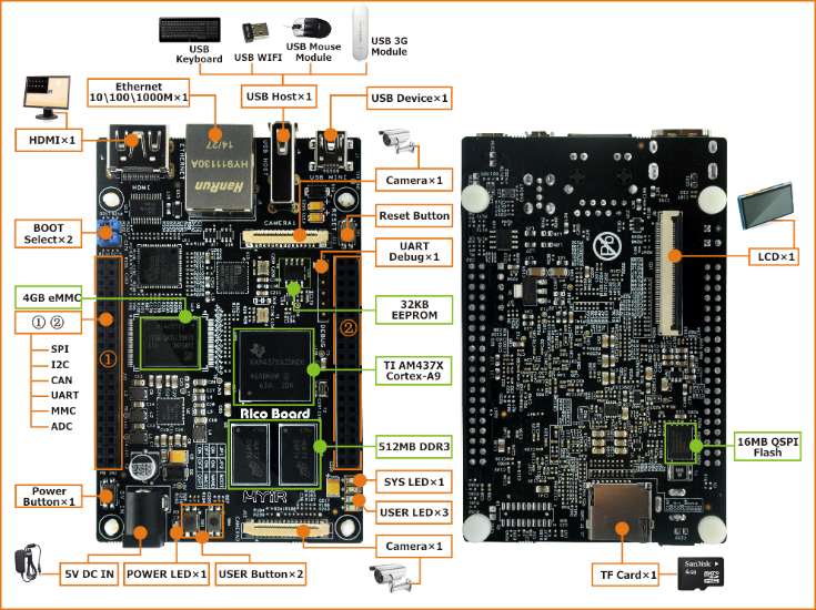
The Rico Board from MYIR is a high-performance single-board computer using TI’s Sitara™ AM437x processors based on ARM® Cortex®-A9 cores. This new generation solution has an increase in performance, as well as extensive reuse from the ARM Cortex-A8 core offerings. Features include:

  • Up to 1GHz of processing power
  • 3D graphics acceleration for rich graphical user interfaces
  • PRU-ICSS for industrial protocols
  • Improved Vector Floating-Point (VFP) unit
  • Other peripherals and interface support like Quad-SPI, dual parallel cameras and  two independent eight-channel ADCs,

 The Rico Board also has many features for optical fiber fusion splicer applications, such as:  

  • Two camera interfaces
  • LCD display interface and buttons
  • Up to ten-channel PWMs from the two 2.54mm pitch 40-pin female expansion connectors
  • The board is capable of running Linux®
  • It can also be a solid platform for evaluating and prototyping for Sitara AM437x processors for optical fiber fusion splicer.

 The optical fiber fusion splicer can use AM437x processors on the Rico Board to control the device. It uses the optical image system which is composed of two high-precision video cameras to extract optical fiber image and then displays the image on an LCD in real time. After that it will calculate and analyze the image through the AM437x processor CPU and provide relative data and prompts. Then using the PWM signal controlled motor, the fusion splicer will make minute adjustments to the fibers’ positions until they’re properly aligned according to the data and prompts; allowing the finished splice to be as seamless and attenuation-free as possible.

During the alignment process, the operator is able to view the fiber alignment through video cameras. After fibers have been properly positioned, the device uses an electric arc to melt two optical fibers together at their end faces, to form a single long fiber. The resulting joint, or fusion splice, permanently joins the two glass fibers end to end, so that optical light signals can pass from one fiber into the other with very little loss. Estimated splice-loss tests are then performed. The whole system consists of six parts:

  •  Optical image system
  • Data processing unit
  • Display system
  • Optical fiber align system
  • Optional fiber fusion unit
  • Input control system

The Rico Board is good for using as the prototype for the optical fiber fusion splicer applications which will be based on TI’s Sitara AM437x solution. The board is also in low cost, pricing only USD.99/pc from the company MYIR which would be affordable for most users.

 To learn more about Rico Board and Sitara processors, visit the below links:


How to protect your server from hot swap events

$
0
0

Need to replace your fan?  Simply trade it out.  Want to add more storage capacity?  No problem – just exchange that 500GB SSD for 4TB. 

But have you ever worried during one of these activities that your server might spontaneously combust?  Probably not.  Unknown to some end users, many modern electronics provide protection against current and voltage spikes during what is known as a “hot swap” event. 

What is hot swapping and why do you care?

Hot swapping is when the user connects an external device or module to expand system capabilities or provide regular maintenance without powering down the host system.  While you see hot swap activity in a variety of applications, protection against these kinds of events is critical in complex systems such as servers.  As you can see in Figure 1, a current or voltage spike from a hot swap event can result in hardware damage, expensive repairs, server downtime, or physical injury to yourself or others. 


Figure 1. Damage to IC due to over voltage and over current events.

Where can this happen in your server?

Many servers are designed to be highly configurable – comprising modules that you can swap in and out as needed including fans, storage devices (HDD and SSDs), and power supply units (PSUs) as shown in Figure 2.  You must carefully consider protection near these modules against hot swap events.


Figure 2. Server components including storage, fans, and PSUs are commonly hot swapped.

Typically, you can place protection against hot swapping events on either the module or the host system as shown in Figure 3.  Due to the highly configurable nature of servers, the host system or backplane vendor is often different from the module vendors.  This makes it difficult to know where protection already exists, but if you are designing a module or backplane, it never hurts to have redundant protection against surges in your server.

Figure 3. You can place hot swap protection on both the host system and module

How can you protect against hot swap events in your server?

There are many options to protect against hot swap events in a server.  Let’s take a look at a few common solutions.

Fuses and polyfuses can serve as low-cost solutions – but a large footprint (shown in Figure 4), degraded performance, and increased maintenance costs can outweigh this benefit over time. 

Figure 4. Comparison of fuse to TI TPS25942 eFuse

Hot swap controllers are another common solution.  These devices provide control logic to an external FET and sense resistor that enable design flexibility specifically when setting RDSON and upper current limits.  However, for many space-constrained server applications, an eFuse can provide the necessary protection and save precious board space by integrating the external components. 

In addition to integration, eFuses add protection features critical for servers.   For example, TI’s TPS25942 eFuse offers common protection features required for a hot swap event including adjustable current limit, over voltage protection, and thermal shutdown, as well as general system protection such as programmable soft start, under-voltage protection, and reverse current blocking.  Should a hot swap event occur, the TPS25942 recovery options include latched and auto retry versions. 


Figure 5. TPS25942 simplified schematic.

Along with its protection features, the TPS25942 also offers system status monitoring by providing outputs to the system for power good, fault, and current monitoring.  With all these features packed in a 3mm x 4mm QFN, it’s easy to see why an eFuse is the right choice for hot swap protection in your server!

So the next time you swap out your fan or install the latest in memory technology – and your super sweet server doesn’t erupt into flames – just remember that it’s all thanks to hot swap protection.  Don’t forget to include an eFuse for hot swap protection in your next server design!

Learn more about designing with eFuses:

How to reduce system cost in a three-phase IGBT-based inverter design

$
0
0

Most three-phase inverters use insulated gate bipolar transistors (IGBTs) in applications like variable-frequency drives, uninterruptible power supplies, solar inverters and other similar inverter applications. Each phase of a three-phase inverter uses a high- and low-side IGBT to apply an alternating positive and negative voltage to the motor coils. Pulse-width modulation (PWM) to the motor controls the output voltage.

The three-phase inverter also uses six isolated gate drivers to drive the IGBTs. Apart from the IGBTs and isolated gate drivers, three-phase inverters include DC bus voltage sensing, inverter current sensing and IGBT protection like over temperature, overload and ground fault.

Cost and performance are challenging trade-offs in many end applications like heating, ventilation and air conditioning (HVAC), solar pumps and appliances.

So what are the best ways to save bill of materials (BOM) cost without compromising system performance? Here are some tactics:

  • Combine the high- and low-side drivers into a single package. A three-phase inverter requires six IGBT gate drivers. You can use individual gate drivers for each IGBT, but a dual-channel gate driver helps with design flexibility and reduces BOM cost.
  • Power the gate drivers with a bootstrap. Needless to say, any high-voltage inverter application will need isolation between the primary and secondary side of the gate driver for reliable operation. The isolated gate drivers may need different supplies for the high and low sides. Instead of using six different isolated supplies for a three-phase inverter, a bootstrap power supply reduces the power-supply requirements to only one, thus reducing total BOM cost and board space.
  • Protect the IGBTs using simple comparators. You can achieve simple overload and short-circuit detection by sensing the current and using window comparators. The comparator output can disable the IGBT gate drivers with the DISABLE function.

TI’s newly released UCC21520 is a reinforced isolated dual channel gate driver. With best in class propagation delay of 19ns (typical), programmable dead time and wide voltage ranges make it really suitable for such inverter applications.

Apart from the IGBTs, the IGBT gate drivers and current sensing play a major role in determining the cost and performance of the three-phase inverter stage. Consider the following tactics save BOM in current sensing circuit:

  • Shunts. Instead of bulky and costly hall and fluxgate current-sensor modules, shunts optimize the cost and space of sensing circuits. Current transformers are also considered but have issues with linearity and performance compared to shunt.
  • In-phase current sensing for better sensing performance (compared to leg current sensing). In-phase current sensing means that there is a constant motor current flowing through the shunt (compared to a noisy switching current in leg current sensing), regardless of which IGBT is switching. Also, it is easy to detect terminal-to-terminal shorts and terminal-to-GND shorts. You can also use two shunts for cost optimization and calculate the current of the third phase in software by using data from the other two sensing circuits.
  • Consider using isolated amplifiers along with a shunt instead of a hall current sensor. Using isolated sigma-delta modulators for current sensing requires digital filters implemented in software or hardware. An isolated amplifier enables interfacing with low-cost microcontrollers with a built-in SAR ADC.
  • Simple overcurrent protection. High-bandwidth isolated amplifiers and comparators with fast response times (<5 to 6µs) enable fast overcurrent protection for inverters, thus allowing you to use cost-effective gate drivers in your system.

AMC1301 is TI’s newly released precision reinforced isolated amplifier. It is optimized for direct connection to shunt resistors and supports accurate current control. The high linearity and low temperature drift of offset and gain errors of the AMC1301 results in system-level power savings and lower torque ripple. With 3µs delay and detection feature of missing high-side supply makes is suitable for motor drives applications.

The new TI Designs Reference Design for Reinforced Isolation 3-Phase Inverter with Current, Voltage and Temp Protection (TIDA-00366) provides a reference solution for a three-phase inverter rated up to 10kW. Figure 1 is a high-level block diagram.

Figure 1: High-level block diagram of TIDA-00366

The design includes the UCC21520 reinforced isolated dual-IGBT gate driver, AMC1301 reinforced isolated amplifier and TMS320F28027 MCU. A lower system cost is possible by using the AMC1301 to measure motor current (interfaced with the MCU’s internal ADC), with a bootstrap power supply for the IGBT gate drivers. The inverter is designed to have protection against overload, short circuit, ground fault, DC bus undervoltage and overvoltage, and IGBT module over temperature.

What techniques do you use for saving the BOM? Tell us.

Additional Resources:

  • White papers:

Industrial stack lights get smarter with LEDs

$
0
0
Light-emitting diodes (LEDs) have many advantages over incandescent lamps, compact fluorescent lamp CFLs or halogen lamps. As a refresher, these advantages include higher lumens/watts, much longer lifetimes, insensitivity to vibrations, instant turn on...(read more)

Eight things to consider when choosing haptic feedback – part 1

$
0
0

As integrated electronics begin to peak, the haptics industry is still in an early age of development. Many people interact with electronics and never think about the feedback transferred from the virtual world of electronics to their tactile senses. We tend to interact more often with electronics through sound. But this interaction is changing, and people want more discreet notifications over distracting ring tones. The vibrate setting on phones or wearable devices enables haptic feedback, but not all haptic feedback is the same.

To provide the most realistic experience, the haptic team at TI created an innovative generation of integrated haptic drivers including the DRV262x family. I will use the DRV2624 and DRV2625 devices as examples when explaining the features you should focus on when selecting your own haptic device. To provide the most realistic feedback using eccentric rotating masses (ERMs) or linear resonance actuators (LRAs), you will need a device that implements advanced haptic effects.

Overdrive, auto-braking, and sine and square outputs

Overdrive and auto-braking significantly improve the haptic experience. For those unfamiliar with these terms, overdrive overcomes the initial inertia required to quickly start an actuator by applying a voltage beyond the rated voltage but limited to a certain “overdrive clamp” voltage. Auto-braking reverses the phase or applies a negative drive voltage to an actuator while monitoring the back electromotive force (EMF) to quickly stop the motor.

When choosing a device, a designer of a mobile application would be interested in sharp braking using open-loop operation. Sharp braking would allow a designer to provide crisp feedback. The DRV262x family enables closed-loop auto-braking out of open-loop mode. This means if you decided to use the open-loop functionality, but still wanted fast braking, devices like the DRV2625 and DRV2624 enable quick braking by detecting a “stop bit” – switching to closed-loop mode quickly and implementing the auto-braking feature.

The newest generation of haptic drivers can switch between sine- and square-wave outputs in open-loop operation. Sometimes actuators respond better to either sine-wave outputs or square-wave outputs over other types of drive signals. You can test both types of signals on the actuator and select the most effective output, an examples is shown in Figures 1 and 2. Flexibility is a key component of selecting a good haptic driver.

 Figure 1: Example square-wave output

Figure 2: Example sine-wave output

One-wire interface

Developers often have to decide between implementing parts based on the number of pins available on their microcontroller unit (MCU). This is why we provide solutions based on one wire. There are two ways to implement the scheme. The first involves tying the NRST and TRIG pins together. Driving both of these pins high at the same time will almost instantly start an LRA (within 1ms). Likewise, pulling both pins low will put the part into shutdown. The second implementation ties the NRST, TRIG and VDD pins together, keeping in mind that the general purpose input/output (GPIO) you use will have to be able to supply the necessary current for operation. Pulling all three lines high at the same time will turn the DRV2624 or DRV2625 haptic driver on and start a haptic effect in less than 2ms. This allows you to implement a world-class haptic driver with a single GPIO.

Solution size

All of these features sound great, but the chip must be large to integrate all of these features, right? Wrong! All of these advanced features are squeezed into one of the smallest packages of any haptic driver on the market. Both the DRV2624 and DRV2625 packages have a total surface area is 2.04mm2, which enables implementation into the mobile space as well as wearable devices.

These first five features are only a few of the recent advancements made in haptic drivers. Next week, I will discuss the final three things you should consider when making your haptic selection. In the meantime, log in and subscribe to Analog Wire to receive alerts through sound or vibration, your choice, when my colleagues and I post a blog. You’ll want to know when part two of this series posts.  

Additional resources

How to reduce acoustic noise of MLCCs in power applications

$
0
0

Multilayer ceramic capacitors (MLCCs) are popular in power electronics designs compared to traditional polymer capacitors for many reasons:

An MLCC provides:

  • A small profile with relatively higher capacitance.
  • Very low equivalent series resistance (ESR).
  • Very low equivalent series inductance (ESL).
  • Lower impedance at higher frequencies.
  • Non-polarization for easier mounting and manufacturing.
  • Higher reliability over time compared to tantalum and aluminum electrolyte capacitors.
  • Lower unit costs.

However, MLCCs do not always sit quietly on the board and do their job. Sometimes they get bored and start to “sing.” This is due to the piezoelectric effect of the ceramic material, which has the same characteristics as other ferroelectric dielectrics. When an electric potential or field applied on the surface of an MLCC causes a deformation at a frequency range from 20Hz-20kHz, it could be audible to humans. This is called MLCC acoustic noise, or singing noise.

Major contributions to acoustic noise include:

  • Electric potential operating at a frequency within an audible range.
  • Smaller case size tends to be lower sound levels than lager case size.
  • Ceramic dielectric constants (K); a higher K has higher ferroelectric properties.
  • Less ceramic layers producing lower sound levels due to less deformation.

 Image courtesy of Murata.com

Figure 1: MLCC and board deformation when applying an electric field

The MLCC itself should be quiet to human ears. However, it can be loud when mounted on a printed circuit board (PCB). Let’s say you had a ceramic capacitor at the input of a switching power converter. The switching behavior creates a high-frequency voltage change on the ceramic capacitor; as the voltage increases and decreases, the MLCC will expand and contract. The deformation of the MLCC creates vibration of PCB, which causes to buzz amplifying. The higher the electric potential change, the larger the deformation (piezoelectric effect), which will result in a louder sound when the frequency occurs in the audible range.

Some applications can use electrolyte or tantalum-type capacitors, preferably thru-hole types when acoustic noise is problematic. But for applications that are more cost-sensitive or size-constrained (such as personal electronic devices), you cannot avoid thin, small ceramic capacitors, and the need to reduce noise immediately becomes critical.

Here are a few available solutions that can minimize or reduce noise to acceptable levels:

  • Use acoustically quieter capacitors. Capacitor manufactures have already developed ceramic capacitors with low distortion dielectric material, which exhibit lower ferroelectric properties and smaller deformation in regards to a voltage change. And there is a series manufactured by Murata that the capacitor is on interposer substrate to reduce the acoustic noise (Figure 2). Murata also has a series with a special mechanical configuration; it uses metal terminals to mount the capacitor on the PCB board to achieve noise reduction by absorbing mechanical impact (Figure 3). Unfortunately, this kind of capacitor tends to be more expensive, which prevents its wide use by end-equipment manufacturers. The effect of noise suppression depends on the type of capacitors. (Figure 4) 

Figure 2: Mechanical configuration of “interposer” ceramic capacitors

Image courtesy of Murata.com

Figure 3: Mechanical configuration of “metal terminal” ceramic capacitors 


Figure 4: Acoustic noise reduction effect by each capacitor (Typical value)

  • Reducing noise by optimizing PCB layout. The origin of the noise is the interaction of MLCCs with the PCB. Optimizing component placement on the PCB can be effective. Using a thicker PCB allows the sound frequency to shift due to weight change. Some articles also suggest placing the components at the edge of the PCB to lower the sound pressure level. Similarly, placing components symmetrically on top and bottom of the PCB can also help to reduce noise level, since the two vibrations will cancel each other out, due to the cancellation-of-vibration effect (Figure 5) when the voltage applies to both capacitors simultaneously.

Figure 5: Capacitors on each side of a PCB to create vibration cancellation

  • Reducing voltage amplitude variation on capacitors. In most cases, end device manufacturing is limited by cost or size, which makes the first two methods described to reduce acoustic noise not practical. However, the other main factor that determines noise is how high or fast the voltage variation is across the capacitors. This is something that can be optimized through proper system design, by either improving the load-transient response or line-transient response.

Considering line-transient response as an example, an experiment was conducted using the TPS51622, one of TI’s DCAP+™ Vcore controllers, by measuring the noise level with a sound meter when varying the output voltage change with fast (48mV/µs) and slow (12mV/µs) slew rates using the Intel voltage regulator (VR) tool. Sending an I2C command to the TPS51622 changes the output voltage from 0.5V to 1.5V, and the input-voltage ripple was measured shown in Figure 5.

Figure 6: Input-voltage ripple on input ceramic capacitors with fast/slow slew rates

The voltage amplitude with a fast slew rate is much higher than with a slow slew rate; this voltage difference across the capacitor directly translates into an increase of noise in decibels. Measured data shows that the noise dropped to a lower, quieter level, from ~40dB to ~50dB. See table 1 for other sound levels and effects.

Table 1: Noise sources and their effects

The wide usage of conventional ceramic capacitors brings acoustic noise issues to power system designs. However, there are solutions that approach the problem from different angles: changing the electronic characteristics of the MLCC itself, or minimizing its interaction with the PCB. These methods either reduce the noise to an acceptable level or remove the noise from the source by using more expensive “anti-noise” capacitors. 

Student determined to honor dying brother’s wish, become 1st in family to graduate college

$
0
0

Ernesto and FelicianoFeliciano Alvarado started planting the seeds of higher education in his younger brother, Ernesto, at a young age. But it wasn’t until Feliciano passed away that Ernesto began to cultivate those seeds.

“My brother was diagnosed with Duchenne Muscular Dystrophy at 10 years old,” said Ernesto, a senior at Lufkin High School in Lufkin, Texas. “It’s a disease that weakens the body’s muscles and then begins attacking vital organs. When I would complain about my coursework, my brother would always say, ‘If I can go through all of this, what’s one night of homework or passing one class?’”

As a middle schooler, Ernesto’s favorite subject was himself, and his favorite pursuit was popularity. This unhealthy obsession landed him multiple stints of in-school suspension and two years of summer school.

Ernesto was in 10th grade right before Thanksgiving when he got the call that his brother had passed away.

“I never took the advice he gave me, even though he’d been planting seeds since I was eight years old,” Ernesto said. “He had this terrible disease, and yet he was able to graduate from high school. I made up my mind right then. I was going to take his advice and become a better student.”

Feliciano getting his diplomaErnesto plans to honor his brother – who was the first in the family to graduate high school – by becoming the first in his family to graduate from college.

GEARing UP to excel in school

Ernesto knew he needed to get serious about his education. When he was in middle school, he would hear his classmates talk about the summer STEM Academy through GEAR UP. 

“It’s a funny story, actually,” Ernesto said. “My friends told me the STEM Academy was fun, there was free food, the opportunity to make friends, and I could get out of my house.”

Ernesto & his friend, DanielShort for “gaining early awareness and readiness for undergraduate programs,” GEAR UP is a discretionary grant program designed to increase the number of low-income students who are prepared to enter and succeed in postsecondary education. GEAR UP provides six-year grants to states, as well as partnerships to provide services at high-poverty middle schools and high schools.

When Ernesto was invited to the GEAR UP STEM Academy, he was delighted to learn his former middle school principal, Vickie Evans, was a GEAR UP director at Lufkin High School. The high school is very diverse and regularly sends the top percentage of its class to elite schools like MIT and Princeton.

“Ernesto is in the top 25 percent of his class,” Evans said. “But school doesn’t come easy for him. He has to work very hard, and he has other barriers in his life. Joining GEAR UP was a turning point in Ernesto’s school career. With the support he’s gotten, his hard work, enrolling in higher-level classes and the tremendous desire to succeed, he’s on the right path.”

Ernesto does not shy away from a challenge. Joining GEAR UP has helped spark a love of math and science in him. He began taking more advanced classes to challenge himself, often asking for extra work to practice outside of class and prescribed homework.

“I played sports as a kid, and my coaches always told me if I ran less laps or did less push-ups, it would only hurt me and my performance in the long run,” Ernesto said.  “That’s why I take on more work. It’s improved my average in math and science, and it’s given me my work ethic.”

Finding time for his studies

Ernesto’s estranged father is a dishwasher. His mother cleans houses and office buildings. As the second in a family of six children, Ernesto stepped up to supplement the family income and save some money by working nearly full time at a local burrito restaurant, preparing food and washing dishes.

“I use my lunch hour at school for homework,” he said. “Sometimes I wash dishes until midnight and head home to sleep for a few hours before school. But it makes me happy that I’m helping.”

Envisioning a career in electrical engineering

Ernesto at TIThough Ernesto’s love of math and science has grown, his classes haven’t become any easier. But he knows what he wants out of his life and future. He learned through TIer Eric Batten, our GEAR UP grant partnership consultant, that electrical engineers are in great demand and that TI is always looking for electrical engineers.

Ernesto dreams of attending the University of Texas at Dallas and working closely with TI research and technology with the hope of eventually joining the team at TI.

“I never knew there was much more to life than working minimum wage jobs until (hearing about electrical engineering jobs at TI),” Ernesto said. “I would not have graduated high school on the path I was on, and now I’m a college-bound high school senior.”

Evans agrees.

“Ernesto will be that kid an employer will want,” she said. “He simply won’t take ‘no’ for an answer.”

Paying it forward

While Lufkin is primarily a blue-collar community, the typical manufacturing jobs have vanished, and students today need to re-think their career paths, Evans said.

“Jobs these students’ parents held are no longer an option,” she said. “We need to help re-invent futures for students, because the factory jobs are no longer there. But engineering and other technical careers are.”

Ernesto wants to influence other students who might be on the same trajectory he was on. As president of Lufkin’s GEAR UP club, he and his friend Daniel – vice president of the club – are planning a “Seed Training Program” for junior high students to share with them opportunities available to them. Ernesto also tells his younger siblings to start creating good study habits now and prioritizing their time.

“There are a lot of things out there most people don’t enjoy,” Ernesto said. “But math and science are everyday things. You need them. Try and keep an open mind. If you don’t love the subjects, try to not be negative towards them. Always give it another shot and turn ‘I can’t’ into ‘I can.’ It might be the start of a big strong tree.”

Tripping Point: Simplifying circuit breaker design using delta-sigma ADCs

$
0
0

In circuit-breaker applications, successive approximation register analog-to-digital converters (SAR ADCs), internal to the microcontroller (MCU) or external, are preferable to delta-sigma ADCs due to their faster startup times. Yet delta-sigma ADCs provide higher dynamic range and higher resolution, an internal PGA (programmable gain amplifier) and consume lower power.

Delta-sigma ADCs have a startup time of ~100ms during power up, which limits their application in circuit breakers. A delta-sigma ADC with a faster startup time is the solution. Using higher-resolution delta-sigma ADCs reduces the need to have multiple hardware for different models of air circuit breakers (ACBs) and reduces design cycle time.

The High Resolution Fast Startup Analog Front End for Air Circuit Breaker reference design (TIDA-00661) focuses on solving critical circuit breaker requirements. You can also use part or all of the solution in molded-case circuit breaker (MCCB) designs.

ACBs for low-voltage applications

Figure 1: SACE Emax 2 air circuit breakers up to 6300A

Domestic, commercial and industrial power-distribution systems use ACBs with integrated electronic trip units (ETUs) for load-side protection.

The ETU in ACB

ETUs provide measurement information also offer functions such as:

  • Fast startup – the trip unit must be operational and begin sampling analog inputs in <5ms.
  • MCU-based true RMS measurement.
  • Current (X 5) and Voltage (X 3) measurement.
  • Making current release.
  • Power measurements.
  • Self-powered when the phase current is >20% to 25% of the nominal current (In) or auxiliary powered (DC input).

For a more detailed description of ETU features, see Section 1.3.1 of the reference design’s design guide.

ACB features : Making current release

ACBs protect power distribution systems/loads against overload, short circuits or earth faults. ACBs are specified in terms of their rated current-carrying capacity; the rated current varies from 200A to 6,300A. The pickup current for the breaker to trip during overload or short-circuit conditions can be set to 10-15 times the rated current, with a maximum rating up to 100kA. Since breakers carry large currents, they have to be protected against closing with faults. This protection feature is called making current release (MCR).

The MCR function trips the ACB if the current exceeds the short circuit or instantaneous pickup-current setting during closing operation. MCR also trips the ACB should an attempt be made to close onto a short-circuit fault current greater than the rated making capacity (50kA, 63kA or 100kA depending on applications, makes and models).

Depending on manufacturer, the breaking time specified is between 30-50ms. Breaking time includes sampling the input current and processing the samples to provide trip commands to the solenoid, which breaks the fault current. This requirement limits your DC/DC converter, MCU and ADC selection.

Reference design features

The reference design contains an AFE board with the ADC and an interface board with MCU and power. It also has a signal-processing front end for an ETU for use with an ACB. This design uses a high-resolution delta-sigma ADC for measuring wide current and voltage inputs within a specified accuracy; the ADC can measure up to eight simultaneous inputs with 24-bit resolution. The ADC interfaces with an MSP430™ MCU for analog input processing.

The design is powered with rectified current input or auxiliary DC input power supplies. It offers two options based on power requirements to generate positive and negative power supplies, one using the LM5017 and the other with the LM5160 configured in Fly-Buck™ mode.

Design features include:

  • Three voltage and five current inputs interfaced to an eight-channel, simultaneous sampling, 24-bit ADS131E08S delta-sigma ADC with fast startup (<3ms).
  • Measurement of AC current input with dynamic range of ≤500 within ±1%, with fixed PGA gain.
  • Measurement of AC voltage input from 10-900V within ±1%, with fixed PGA gain.
  •  DC/DC converters in the Fly-Buck converter configuration to generate supply outputs.
  • Subsystem configurable for 2W or 8W power outputs.

Reference design advantages

The ADS131E08S delta-sigma ADC-based reference design fulfills some of the critical requirements of ACBs, such as:

  • Fast startup: ACBs are specified to trip within 30-50ms when powered with a fault. The  time includes system power up, AC input current measurement and breaking of the fault current.
  • Wide-input measurement: The fault current input range varies from 0.3-15 In (nominal current) or more for a given current-breaker rating. The circuit breakers are available in multiple current ratings. An ADC with high resolution ensures the use of the same ETU for multiple current ratings or all current ratings with no hardware changes. Similarly same ETU can be used for multiple Voltage rating simplifying the hardware design and testing.  The wide input measurement is achieved by high resolution ADC, PGA and Reference that can be set to 2.4V or 4V resulting in increased dynamic range.
  • Accurate measurement of voltage and current inputs: The accurate measurement of input current ensures a repeatable trip-time performance for protection and accurate measurement of different parameters for metering. Accurate measurement is achieved by the High resolution ADC, internal PG and internal reference.
  • Increased reliability and temperature performance: The integration of reference and PGA reduces external component requirements, improves temperature performance, and increases reliability.

Table 1 lists the startup delay for the reference design’s various subsystems.

Table 1: Startup Delay for ACB ETU TI design

The reference design has been tested for voltage and current accuracy performance over a wide range of current and voltage inputs.  Accuracy of ±0.5% was achieved for 1 cycle measurement (80 samples @ 4000 samples per cycle for 50Hz input) See Section 8 of the reference design’s design guide.

Summary

The ADS131E08S delta-sigma ADC-based reference design TIDA-00661 solves critical system design challenges for ACBs using delta-sigma ADCs and improves measurement accuracy for half- or one-cycle measurements. It comes with the design guide, Altium schematics and printed circuit board (PCB) files, assembly files, and a bill of materials (BOM) for accelerating your design.

Additional resources:


Use a dedicated parallel charger for cost-effective fast charging

$
0
0

Today, system designers need to be much savvier about power management. Because of the ever-increasing number of functions and applications, there are greater demands on battery capacity. Users also demand shorter charge time, which requires faster charge currents.

A single charger may not be able to support the high charge current needed, however, because of the thermal limitations in semiconductor packages. Nobody likes handling a hot device. By adding a secondary charger in parallel with the main charger, you can boost the total charge current by 75%-100%. This is called a dual-charger system. It is generally a better solution for supporting charge currents greater than 5A and distributing heat across the board.

Generally speaking, a dual-charger system includes a main charger and a parallel charger. As you can see in Figure 1, the main charger takes control for the entire charging process, while the parallel charger is disabled by default and usually only operates when a high charging current is necessary.


Figure 1: Dual-charger system simplified block diagram

It is not necessary to use two full-featured charger ICs for a dual-charger application. A dedicated, specially designed parallel-charger IC still does the job well and saves component costs, since a parallel charger does not need all the functions of the main charger. As a dedicated parallel charger, its charge should be disabled by default and activate only when necessary. Table 1 compares the key features of a main charger and a dedicated parallel charger.

Table 1: Main charger and parallel charger feature comparison

As an example, a dual-charger system could be implemented with two bq25890 devices in parallel. These devices are in a 4mm x 4mm package. However, the second charger does not require many of the functions as shown in the table above. By using a bq25898C as the parallel (second) charger with smaller package, the total system cost and PCB space required can be reduced.

Consider using parallel charger when implementing fast charging into your design. This design consideration helps manage thermals when handling higher charge current, thus charging your devices faster and more efficiently. For more information about dual charger design, see the user’s guide for the bq25890 and bq25892.

How to power your thermostat using solid state relays

$
0
0
Co-authored by Miro Oljaca and Tattiana Davenport If you read my previous blog post, “ Click! Clack! What’s the setback in your thermostat? ” about the interaction between a thermostat and a heating, ventilation and air conditioning...(read more)

Go differential to differentiate your precision design

$
0
0

While more of the industry’s newest high-resolution, precision analog-to-digital converters (ADCs) implement differential inputs to maximize performance, many designers still choose to use single-ended amplifiers because that’s what they’re comfortable with. But low-power fully differential amplifiers (FDAs) offer many system advantages without sacrificing precision. In this post, I will use the new THS4551 low noise, precision, 150MHz FDA as an example of how to realize many of the benefits of fully differential amplifiers.

FDAs enable simple single-ended to differential signal conversion with direct current (DC) coupling. In Figure 1, you can see three different examples of driving a single-ended signal into the differential input of an ADC. However, the FDA offers lower power, lower noise and an improved dynamic range.

(a)(b)(c)

Figure 1: Pseudo differential input (a); dual operational amplifier (op amp) method (b); and fully differential amplifier method (c)

The FDA architecture can help significantly lower total harmonic distortion (THD) by reducing HD2. Implementing the FDA method shown in Figure 1c, you can achieve an improvement of >4dB in THD.  This >4dB improvement can result in an overall system performance improvement, or give you the flexibility to use a lower-power/lower-bandwidth amplifier to meet the same THD.

A single FDA (Figure 1c) will have 1/√2 lower noise for the same power than a pair of single-ended op amps (Figure 1b). For example, an op amp with an input-voltage noise of 3nV√Hz will have a total input-voltage noise of 3*√2 nV/√Hz in the dual op amp circuit shown in Figure 1b.

The FDA can operate from a single supply voltage and still accept bipolar input signals. Figure 2 shows the THS4551 accepting a 20Vpp input (0V common mode) and outputting 8Vpp with a 2.5V common mode. This capability allows you to reduce system complexity by eliminating the negative power supply and any unnecessary signal-attenuation stages.

Figure 2: FDA attenuation example

FDAs include a common-mode output loop to perfectly match the expected ADC input common mode. The Vocm pin sets the output common mode of the amplifier. You can leave this pin floating if your desired common mode is at the midpoint of the supplies.

As shown in Figure 3, TI FDAs are offered in a number of small packages including 2mm-by-2mm QFN, making them suitable for use in even the most space-constrained application.

(a)(b)(c)

Figure 3: 2mm-by-2mm 10-pin QFN (a); 3mm-by-3mm 16-pin QFN (b); 5mm-by-3mm 8-pin VSSOP (c)

TI’s new THS4551 is one of the highest-precision FDAs in the industry, with ±0.175mV input offset and <2V/C offset drift. This enables the improved system performance and minimizes the need for costly and time-consuming system calibrations.

The evaluation module (EVM) for TI’s new ADS127L01 24-bit 512Ksps delta-sigma ADC offers an example of the power of FDAs. The EVM for the ADC implements an ADC driver using the THS4551 configured as a multifeedback (MFB) filter. As Figure 4 shows, the ADC-plus-driver pair achieves a signal-to-noise ratio (SNR) of 110.6dB and a THD of 119.1dB with a 1kHz input signal. As shown in the ADS127L01 data sheet (and the goal of all ADC driver implementations), the performance of the THS4551 does not have any impact on the performance of the data converter. This level of performance was achieved while adding less than 7mW of system power, making the THS4551 an essential part of designs that require the lowest power while also delivering the best harmonic distortion and precision.

Figure 4: ADS127L01 with THS4551 spectrum

If your ADC has a differential input, a precision FDA, such as the THS4551 could be a good choice to simplify your system design and enable low noise, low power, and low harmonic distortion. What is your experience designing with FDAs? Login and leave a comment below about your experience.   

Additional resources

Kickstart your design with DLP technology

$
0
0
It’s the time of year when everyone is starting to gear up for another school year and all that entails. The beginning of the school year represents a fresh start, new ideas and an influx of learning. With this in mind, we started thinking about...(read more)

How Bluetooth® 4.2 can help enable product security

$
0
0

With the release of the new Bluetooth® low energy software development kit (SDK), BLE-Stack 2.2 software, TI is offering a completely new level of security as indicated in the Bluetooth 4.2 Core Specification. But what exactly do these security improvements mean, and why are they being rolled out now?

There are two independent security upgrades that come with Bluetooth 4.2:

  1. Secure pairing
  2. Privacy

Secure pairing

Pairing is the process of setting up a connection between two Bluetooth devices that need to exchange information through some form of defined relationship. In many cases, this information is of little value to other parties who might be within receiving range of the RF packets being exchanged over the connection. But as Bluetooth moves from the smartphone ecosystem to the Internet of Things (IoT), where home and building automation as well as automotive and medical/health applications require the transfer of information that could lead to serious consequences if intercepted or altered by attackers, it becomes vital to offer a secure connection where the confidentiality and the integrity of the data is ensured by adherence to a common standard. This is what Bluetooth 4.2 brings to the table.

Securely encrypting the packets transmitted between two devices in a connection is quite straightforward as long as they both share a secret key. AES-CCM is the encryption technique used in both Bluetooth 4.2 and earlier standards. But this technique does not provide a way for two devices that are being paired by their owner to exchange a secret key that cannot be read by passive eavesdroppers several meters away. This is the big improvement in Bluetooth 4.2, where the Elliptic Curve Diffie-Hellman (ECDH) key agreement protocol is introduced. ECDH is today’s gold standard in key agreement schemes, and allows two parties with no previously shared information to establish a secret key that is known to them only. Sniffers who have observed the exchanged packets will not be able to “guess” the shared key. This is made possible by the asymmetric key properties of Elliptic Curve Cryptography (ECC), which allows both parties to have one public key and one private key. A packet encrypted by device 1’s private key and device 2’s public key can only be decrypted by device 2, using device 2’s private key and device 1’s public key. Device 2 will then know that the packet could only have come from device 1, and could not have been read by anyone else. The same method is used to transmit from device 2 to 1, using device 2’s private key and device 1’s public key. This is still an anonymous exchange and does not prove the identity of device 1 or 2. Identity proof, if needed, can be added at the application level by letting device 1 and 2 exchange certificates that prove their identity based on their public keys.


Figure 1: Device 1 sends an authenticated and private message to device 2. Only device 2 can read it, and only device 1 could have sent it, as it needs device 2’s private key to be decrypted, and was encrypted using device 1’s private key

Privacy

In order to enable pairing with new devices, Bluetooth low energy peripherals will send out connectable advertisements with regular intervals. If they stop transmitting advertisements, they will never be able to establish a new connection again, so this activity is continued throughout the lifetime of the device. These advertisements contain the information a scanning central (e.g. a smartphone) needs to initiate a pairing process with that peripheral. That includes the Bluetooth Device address (BD address), which uniquely identifies that peripheral. This makes it very simple to track peripheral devices and log their position. Passive observers need only to listen for advertising peripherals, log the BD addresses and forward them to a data processing center that receives BD addresses from many observers. In this way, peripherals can be tracked anywhere an organization has set up observers. And since more and more of these peripherals are constantly worn by their owners, it is effectively the owner who is tracked and not just the peripheral. For retail chains, this can help them analyze how customers move around in their stores or even between stores. This collection and use of information is in most cases harmless, but the ease with which this type of tracking can be set up means that there are many organizations that will be capable of doing it, as they do not need to be particularly resourceful or technologically advanced.

This problem is solved with the privacy enhancements in Bluetooth 4.2 and the solution is quite simple: The Bluetooth 4.2 peripheral devices regularly choose a new and random BD address to use in their advertisements. Only after a connection is set up with a trusted master, is the peripheral device’s real BD address disclosed. Observers wanting to track advertising Bluetooth 4.2 peripherals will have no way of resolving the real BD address based on the randomly chosen advertising address and tracking the random address will only last until the device choses a new one.       

Summary

Bluetooth 4.2, as implemented in TI’s BLE-Stack 2.2, offers significantly improved security and privacy, allowing Bluetooth developers to deploy devices that can enter secure connections without being intercepted or tracked by observers.  To incorporate these security enhancements into your Bluetooth product, check out TI’s SimpleLink™ Bluetooth low energy CC2640 wireless microcontroller (MCU).  

 Where to go next?

Viewing all 4543 articles
Browse latest View live


<script src="https://jsc.adskeeper.com/r/s/rssing.com.1596347.js" async> </script>