Quantcast
Channel: TI E2E support forums
Viewing all 4543 articles
Browse latest View live

Take Charge of Your Future: Reimagining the TI Innovation Challenge in India

$
0
0

The next generation of STEM innovators in India will come from our engineering student community who wants to build solutions to local as well as global problems. These students want to chart their own course, pursue their own ventures and aspire to innovate for the future and change the world with their ideas. 

The TI India Innovation Challenge Design Contest (IICDC) is a platform where these  young engineering students can use their scientific curiosity and technical skills to usher in a new era of tech-led entrepreneurship in India. Innovations led by these young entrepreneurs will catalyze the manufacturing ecosystem in India, in line with the vision of the government’s Make in India campaign. This year the IICDC has partnered with India’s top business school, the Indian Institute of Management Bangalore (IIMB), and the government’s Department of Science and Technology (DST) to bring the right combination of technical guidance, business mentoring and government support to inspire an entrepreneurial spirit that drives students from idea to invention to industry, helping them become successful entrepreneurs.

Here’s how it works:

With TI’s collaboration with DST and IIMB, the India Innovation Challenge allows engineering students to join an ecosystem encompassing government, academia and industry. This ecosystem will provide support to students as they begin to explore innovative ideas. Some of this support includes:

  • Tools: TI tools worth INR 13,000 ($200 USD) to implement their idea
  • Technical Guidance: Access to technical resources on TI.com and direct access to engineers through the  Engineer-to-Engineer (E2E) forum
  • Business Mentoring: IIMB, with its immense experience in business and marketing, will guide teams to transform the best ideas from the contest into successful enterprises
  • Funding: DST will provide a seed fund of INR 2Crores ($300,000 USD) and product development fund of 1.5 Crores ($220,000 USD) to be distributed among the top teams of the contest 
  • Cash Prizes: INR 50Lakhs ($75,000 USD) worth of prizes to be won in the contest

The best part: the new TI Innovation Challenge in India offers these resources to all students who participate in the contest, which last year, totaled to 11,000 Indian students from 650 engineering colleges. The contest helps students get started in a competitive marketplace, providing the training wheels most entrepreneurs do not have the luxury of getting before going to market with their idea.

Once students have submitted their ideas for the competition by September 30, 2016, the teams will be evaluated against the qualifying round criteria and select teams will receive TI tools worth $200 USD to implement their idea. The top 10 teams from the contest will enter the IIMB’s reputed incubation center, the Nadathur S. Raghavan Centre for Entrepreneurial Learning. This center will offer the teams two years of mentoring to develop their business.

If you have an innovative idea, a dream to create something new, and the ambition to make a difference, then we invite you to participate in the India Innovation Challenge 2016. Enter the India TI Innovation Challenge design contest by September 30, 2016 for your chance to launch your own startup.

For more details, visit www.ti.com/iicdc  | email: ti-india-dc@list.ti.com


USB Type-C: Enabling adoption of new standard for electronics

$
0
0

The days of carrying around multiple chargers and accessories for your smartphone, laptop and other electronic devices may be coming to an end, thanks to the next-generation universal serial bus called USB Type-C.

USBTYPE-CImagine charging all of your electronics with a single cable, powering your laptop battery as you drive to that next meeting, and simply plugging your notebook into a colleague’s laptop to share a presentation. These are just some of the capabilities of USB Type-C, which is expected to become the standard for electronic devices.

We are not only pushing the world forward with this innovation, but we are also helping our customers adopt the new technology.

“We’re creating a new paradigm in the way we coexist with our electronic devices,” said Kevin Jones, a marketing and applications director in our Analog business. “The ICs we are bringing to market will enable changes in how we use notebooks, docks, PCs and accessories. This technology is allowing us to do things we’ve never done before.”

We are making it easy for designers to make the transition with products like our multi-port USB Type-C and power delivery mini-dock reference design (TIDA-01243), which we launched today.

“TI is making every effort to make it easier for designers to implement USB Type-C into their designs,” said Irene Deng, a power management product line manager. “Each product is released with a simple-to-read, yet thorough, datasheet and a complete system design. This enables designers to not only try it out but also quickly adopt it in their designs.”

The new mini-dock represents our full ecosystem of USB Type-C power delivery solutions including at least 20 TI devices, including the USB hub in the design, electrostatic discharge protection for every port, audio coding/decoding capabilities and DC/DC converters.

“We offer the industry’s most complete portfolio of USB Type-C compliant products and resources to simplify the design process and speed time to market,” said Keith Ogboenyiya, a general manager in our Analog group. “As a result, we are making it easier for designers to implement USB Type-C into their designs.”

Learn more about the mini-dock.

Period of change

The effort to standardize USB connections started about three years ago when we were trying to find a way to combine video and data into one cable. In partnership with a consortium of other experts, we realized we could combine data, video and power into one cable using a universally recognized connection. The first USB Type-C standard came out last year.

We are now in a period of rapid change to adopt the new USB Type-C technology, Irene said.

“Nowadays, we use various handheld devices in our personal and business life around the clock,” she said. “Consumers of these devices hunger for simpler and faster power charging and data communication features. USB Type-C technology is feeding this hunger.”

Kevin and Irene say they are most excited about the way our new products will change the way consumers coexist with electronics. First off, we will be able to power all of our compatible devices using one USB Type-C cable, and vice versa.

“USB Type-C is going to make everyone’s lives much simpler and hassle-free. We will no longer worry when our cell phone runs out of power while we rely on the map to tell us how to get to the hotel,” Irene said. “USB Type-C charging ports will be available everywhere we go. All we will need is one charging cable for our different devices.”

USB Type-C will impact everything from personal computers and mobile phones to PC accessories like docks, dongles and monitors. You will see large docking stations shrink to the size of pocket-size TV remote controls. Smartphones will become even thinner and will charge quicker at higher voltages – possibly up to 20 volts compared to the current 9-12 volts.

“When that ecosystem exists, there will be a strong need for Type-C and power delivery in a car. The simple use case will be a very capable charging port that coexists with legacy systems,” Kevin said. “The way your infotainment system in your car reacts with your laptop and phone can be much more dynamic.”

Infotainment systems incorporating Type-C and power delivery can communicate to a laptop or phone to negotiate a variety of power contracts to ensure each device is charged as quickly as possible, he explained. On the data side, the infotainment system can also dynamically change from receiving content to providing it, and vice versa.

Learn more about USB Type-C and power delivery. Also, look for several other USB Type-C devices coming out this year.

Additional resources:

How to design current sensing and protection with off-the-shelf op amps

$
0
0

Protecting expensive, critical or hard-to-repair equipment against overcurrent and power-supply fault conditions can be achieved with universally available operational amplifiers (op amps) and a few external components.

In this post, I will present one example of a versatile variable load-current detection/protection scheme that you can easily alter for a large range of load currents, as it has ubiquitous op amps at its core.

“Variable” refers to the benefit of having a nominal “operating” power-supply load-current limit (I_load) that drops on demand. An example would be if you needed to throttle the main system’s power-supply current limit in a transient power-up condition before one or more other supplies have reached their nominal voltage. In Figure 1, if Vref (which represents another monitored power supply) is below nominal (Vnom), the load current drops for safety or reliability reasons. With Vref less than Vmin, the load current pinches off (I_pinch).

Figure 1: Load current is a variable function of another supply voltage (Vref)

Once Vref is at Vnom or higher, normal I_load limit is permitted to flow.

Figure 2 uses the versatile LM7301 rail-to-rail input and output op amp to implement the load current limit profile shown in Figure 1. The circuit monitors the Vsupply current to the load. When the current exceeds the limit determined by the Vref voltage, it produces an output that turns Q1 on and can trigger a protection mechanism. The op amp’s large operating supply voltage (1.8V to 32V) simplifies the design task by extending the range of usable supply voltages (Vsupply) monitorable for load current. In addition, a full-range output swing eases the output drive (on/off) to the gate of a protection transistor or MOSFET (Q1 in Figure 2). Since the input common-mode voltage range extends from below ground to above V+, you can tie the high-side sense resistor (Rsense) directly to the op amp inputs.

U1A, which monitors Vref, must have an output swing close to Vsupply in order to allow the kind of behavior depicted in Figure 1, where a reduced Vref pinches off the allowable load current. Furthermore, you could use the same op amp as an amplifier (U1A) or comparator (U1B) to reduce the bill of materials (BOM).

 Figure 2: Variable current-limit detector

The circuit operates by passing all of the load current through a single sense resistor (Rsense), with U1B monitoring both terminals. Enough load-current flow will cause the U1B output to switch high toward the Vsupply rail, which then could turn on a protection device such as Q1. U1A monitors Vref; its output changes the voltage that appears on the non-inverting input of U1B. A low Vref voltage raises U1A output and reduces the I_load value that triggers the U1B output high (fault condition), and vice versa. Diode D1 turns on when U1A detects Vref approaching Vnom and prevents any further increase in I_load with increasing Vref voltage (see Figure 1, where I_load is maintained for Vref ≥ Vnom). The hysteresis resistor R7 works with other external resistors to set the amplitude of the hysteresis, which introduces a difference between the load current that initiates overcurrent and the load current that resets overcurrent. This difference in currents ensures that the circuit does not enter an unstable condition where the U1B output chatters back and forth.

At a 4MHz gain-bandwidth product, the op amp can respond to fast current transients if necessary. However, capacitors C1 and C2 can slow down the circuit response time so that transient current spikes do not trigger the overcurrent limit detection – such as those encountered at startup when the supply decoupling capacitors draw excess current to reach their operating voltage.

Here are some of the governing equations that make it easier to modify the circuit for different operating conditions. I’ve also included an example operating condition to allow numerical results using the component values shown in Figure 2.

Vsupply = 12V

Vref = 5V (Vnom condition)

To find the current limit as a function of Vref (or U1Aout):

When Vref drops, U1A output moves high until U1A output saturates with the values shown. Vmin corresponds to the Vref voltage where the U1A output has saturated high. For a rail-to-rail output device, that means:

To find the Vmin in Figure 1:

Calculate Vmin with Equation 3 and rearrange Equation 1 to solve for Vref as Vmin:

Any lowering of Vref below Vmin has no effect on the load-current limit, which is already pinched off (I_pinch). For the LM7301, the saturated U1Aout voltage is about 100mV lower than Vsupply, or:

To find I_pinch in Figure 1, plug the information from Equation 5 into Equation 2:

To find the amount of hysteresis in the load current detection point:

So lowering the value of R7 increases hysteresis proportionally.

Increasing Vref beyond Vnom is clamped by D1 such that the load-current limit remains constant. The value of Vref when this occurs has to do with the voltage divider set by R12 and R13. With the values shown in Figure 2, the D1 anode is set to 8.7V and starts conducting when Vref ≥ 5V, thus establishing Vnom=5V. The voltage divider resistor values should be low enough to supply the current to keep D1 forward-biased with U1Aout saturated to ground.

Once you have all of the governing expressions for the most important operating points of the circuit, you can easily modify it to fit your intended application. Having a versatile op amp as the main active element in a system can offer added flexibility in setting the operating conditions and load current profile. As an added benefit, it is possible to have more than one supply voltage throttle the load current; just add a series resistor from these other supply voltages to the U1A inverting node, similar to Vref.

What considerations do you face when protecting equipment against overcurrent and power-supply fault conditions? Log in to post a comment or visit the TI E2E™ Community Precision Amplifiers forum.

Additional resources

Step by step: How the series capacitor buck converter works

$
0
0

My cousin introduced me to the Texas two-step a couple years ago. I enjoyed swing dancing in college but had never tried two-step before. My first few attempts were quite abysmal. Fortunately, I was with friends and we could laugh about it. After several more tries, I was able to get the hang of it.

It can also be a little daunting to learn a new converter topology.You might be familiar with the conventional buck converter. The simplicity and beauty of this converter has made it popular for decades. TI recently introduced the TPS54A20 based on the series capacitor buck converter. It is a new topology that enables efficient, high-frequency operation of small point-of-load voltage regulators.

Figure 1: Thetwo-phase series capacitor buck converter

Today we are going to learn the “steps” of the series capacitor buck converter shown in Figure 1. Like any new dance, it may be challenging at first. After walking through the steps of steady-state operation a few times, I think you will find that it is not that difficult. You might even like it! This will be a brief beginner’s class; if you want more details, check out this application note. So let’s begin by considering a converter with a 12V input switching at 5MHz per phase.

The first step, or time interval, occurs when the high side switch of phase A (Q1a) is on as shown in Fig. 2. The series capacitor (Ct) connects to the input by switch Q1a. Because the nominal voltage across the series capacitor is half the input voltage (approximately 6V in this case), the phase A switch-node voltage (VSWa) is roughly half the input voltage, shown in blue in Figure 2. The phase A inductor current (ILa) rises in a triangular fashion just like a normal buck converter (no resonant behavior) and simultaneously charges Ct. In fact, the series capacitor current (ICt) is equal to ILa during this step. The differential series capacitor voltage (VCt) increases by a few hundred millivolts due to the added charge. During this step, the phase B low-side switch (Q2b) is on, connecting the phase B switch node (VSWb) to ground. The phase B inductor current (ILb) decreases linearly as a result.

Figure 2: High side switch of phase A (Q1a) on (step 1) 

Both low-side switches (Q2a and Q2b) are on during step two, as shown in Fig 3. This connects both VSWa and VSWb to ground just like a conventional two-phase buck converter. Both ILa and ILb have negative slopes. Because the series capacitor has no current flowing through it (because ICt is zero), VCt remains constant. 

Figure 3: Both low side switch on (step 2)

Step three is where things get interesting, so pay attention to Fig. 4. Switch Q2a is still on, connecting VSWa to ground. Switch Q2a is also connecting the negative side of Ct to ground. When the phase B high-side switch (Q1b) turns on, the positive side of the series capacitor connects to VSWb. Now the series capacitor is acting like an input capacitor for phase B! ILb ramps up and simultaneously discharges the series capacitor. This is evident from the negative ICt and the small decrease in VCt. ILa continues to ramp down.

Figure 4: High side switch of phase B (step 3)

Step four is identical to step two as shown in Fig. 5. Q2a and Q2b are on and VSWa and VSWb are grounded. Both ILa and ILb ramp down. VCt remains fixed because ICt is zero. After step four, the whole cycle repeats.

Figure 5: Both low side switches on (step 4)

How was that? Not too hard, right? Check out the additional resources to learn more about this exciting new topology. Now it’s time to hit the design floor and take the series capacitor buck converter for a spin.

Additional resources

Smart power banks support high voltage charging

$
0
0

Power banks are becoming more and more popular as battery capacity outstrips the runtime of personal electronic devices like smartphones and tablets. High-performance CPUs, large sizes and high-resolution display panels also make runtimes shorter. This creates an demand for a fast-charging backup battery such as a power banks.

Traditionally, a 5V USB is the standard power supply for mobile devices like smartphones and tablets. Due to the current capacity limitation of mini USBs, a 5V power supply can only deliver about 10W of power at best, which could take more than 6 hours to charge. With the battery capacity of mobile devices increasing, long battery charging times become a headache for consumers.

To improve the user experience, high-voltage (>5V) charging method  provides more input power and shortens charging times,  while maintaining the same cable current of 2A. Beyond high-voltage charging, many power-bank vendors are also creating more intelligent power banks through the integration of a battery fuel gauge, which allows users to see power-bank status and estimated charge and discharge times  A trend is to get the power bank to be smarter. It enables users to be informed of the status of power bank, estimate the charging and dis-charging time.  Authentication is also becoming a trend, where the end application and power bank require authentication before charging. The idea is to preserve the overall battery life of the application.

Power-bank designers in Asia are some of the early adopters of these up-and-coming features; one leading power-bank vendor in China uses TI’s 2.4 GHz CC2543 system-on-chip (SoC) and bq25895 in its new designs. In the vendor’s case, the input needs to support 12V/9V/5V adapters with a 4A maximum battery-charging current, while the output discharging power is 5V/2.1A.

Figure 1 is a typical block diagram of a smart power bank. The 8051 core, 32kB flash, 1kB RAM CC2543 SoC acts as the system controller as well as the wireless transceiver. The key factor in this design is using the CC2543 device’s proprietary radio to achieve low power and low-cost Bluetooth® Low Energy beacon functionality.

The bq25895, a single-cell fast-charger provides a handshake with the adapter autonomously and supports high-voltage charging (buck). Its charging current can be as high as 5A. When in USB On-The-Go mode, the bq25895 can work as a boost and output a stable 5V (with a maximum output current of 3A) for powering a connected end device like a smartphone.

The TPS2514 USB-dedicated charging port controller provides a handshake with the connected device to make sure that the device can extract the maximum power from the power bank.

Figure 1: Block diagram from a smart power bank supporting high voltage charging

Several companies have provided different protocols for high voltage charging, including TI. More and more smartphones and power banks now include a high-voltage charging feature. In this fiercely competitive market, the bq25895 and CC2543 SoC can bring extra value to enable full fast-charging capabilities and increase the quality of your products. Learn more about the benefits by visiting the product folders and let us know what you’re looking to design fast charging with in the comments.

Additional resources


Inductive sensing: How can an inductive switch be used for lid open/close detection?

$
0
0

A customer recently asked me to optimize a lid open/close detection mechanism for a consumer product. To avoid relying on potentially unreliable electrical contacts, magnets or expensive optical solutions, I suggested the LDC0851 differential inductive switch.

Today I want to show you how to use an inductive switch for this purpose and how a threshold adjustment feature can help set the switching distance.

How can an inductive switch be used for lid open/close detection?

Typical inductive proximity-sensing applications use a small metal target such as a piece of copper foil or even a screw to detect the position of a moving part such as the lid or a door of a consumer product, as shown in Figure 1.

Figure 1: Lid open/close detection application


To determine if metal is present, the switch compares the inductance of a sense coil to the reference coil. The outer coil diameter determines the maximum switching threshold.

I suggested a stacked coil approach, in which printed circuit board (PCB) layers 1 and 2 contain the sense coil and layers 3 and 4 contain the reference coil. Figure 2 shows a system block diagram.

Figure 2: System block diagram


When should I use threshold adjust mode?

In proximity applications, it is important to determine if the LDC0851 should operate in basic operation mode or threshold adjustment mode:

  • In basic operation mode (ADJ = 0), the LDC0851 uses a reference target positioned at a fixed distance from the reference coil and a moving target over the sensor coil. Unfortunately, the reference target is not easy to add in this system.
  • You must use threshold adjust mode (1 ≤ ADJ ≤ 15) if there is no fixed target present near the reference coil. In this mode, the reference coil inductance has an offset subtracted to alter the switching threshold. Operating in threshold adjust mode ensures that the sense coil inductance is greater than the reference coil inductance at an infinite target distance, and therefore that the release point is well defined. This is the case in both stacked coil applications and side-by-side coil applications. Within threshold adjust mode, ADJ = 1 produces the largest sensing range and ADJ = 15 the smallest, as shown in Figure 3. Note that the switching distance is also a function of the outer coil diameter.

Figure 3: Different ADJ codes affect the switching threshold


Configuring the LDC0851 for threshold adjust mode requires setting a resistor divider on the ADJ pin. The ADJ pin has 16 levels (level 0 disables the threshold adjust feature, and is equivalent to basic operation mode). The LDC0851 data sheet contains the recommended resistor values for each level. Figure 4 shows how the lid height and ADJ code affect the adjusted coil inductance. 

Figure 4: Lid height vs. coil inductance and ADJ code


With the LDC0851, I was able to help the customer with a simple and reliable solution. Not all inductive proximity-switch applications have a metal target near the reference coil to set the switching point, however. In applications without a reference target, the threshold adjust mode ensures that switching occurs at the desired target distance. What’s your experience designing with inductive switches? Login and leave a comment below.

Additional resources

Enhance your home automation project with an LED driver

$
0
0


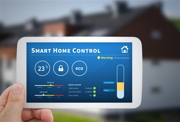
The smart home is no longer just for movie and millionaires. New products are hitting the market every day to connect you to every part of your house. There are products to turn on your lights from the other room and you can even find a device to monitor your dog from afar. With advancing technology it’s now easier than ever to create your own automated system using a microcontroller. You can even add light emitting diodes, or LEDs, for visual feedback and status indication! In this blog, we’ll take a further look at designing LEDs for home automation designs.

When you’re first taught to use a microcontroller with higher current LEDs, you’re taught to use a transistor for the input control, and to place a resistor in series with the LED to set the forward current. This is fairly simple to do with a single LED, but adding additional LEDs takes up a lot of space. Soon, you will be looking for a bigger microcontroller with more general-purpose input/output (GPIO) pins. This becomes costly and requires more processing effort to control the multiple LEDs.


Figure 1: A discrete implementation to drive an LED using a microcontroller unit (MCU)

LED drivers help solve this problem by simplifying the control of multiple LEDs. They also add to the overall solution by adding features such as blinking, pulse width modulation (PWM) dimming, and error detection. A home automation system can communicate its status to the user using the blinking and PWM signaling using the functionality of the LED driver instead of relying on the microcontroller.

One of the biggest advantages of using an LED driver over traditional current setting resistors is the ability to control a large number of LEDs with minimal GPIO pins. TI’s TLC59116 I2C LED driver can control 16 different channels on a single device using only three microcontroller pins. The four hardware address pins allow the user to go from 16 channels to 224 channels using the same three pins. This means that as the home automation project becomes more complex, the number of LEDs needed to communicate the device status can be scaled as needed.

Figure 2: Multiple TLC59116 can be added using the same SCL, SDA, and RESET pins.

Not only can the number of GPIO pins for the microcontroller be minimized, the processing effort required by the microcontroller to create the LED effects can also be reduced. The TLC59116 supports both PWM dimming and blinking of LEDs using internal frequency control. Combined with the functionality to set every LED at the same time, the TLC59116 can control a variety of LEDs using basic I2C commands.


So how will you enhance your home automation project? Maybe you want to warn that a room is getting too cold, or notify that your favorite pet hasn’t been fed. Feel free to add some RGB LEDs for status indication. Multiple pets? Add more LEDs to make sure that no puppy goes hungry. With LED drivers like the TLC59116, you can scale your project with ease!


Additional resources:


Haptics-enabled cane, blind spot detector among top intern DIY projects

$
0
0

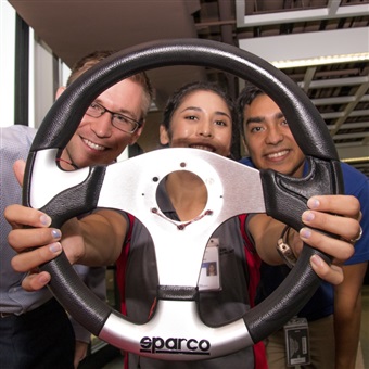
Intern DIY blind spot detectorWe love the can-do spirit that lies at the heart of our makers. And we encourage it in our summer interns.

Take Micah, Erick and Maria for example. For our 2016 DIY with TI – Intern Edition event, this inventive crew built a blind spot detector. The creative contraption uses an ultrasonic sensor in a car’s blind spot regions to alert the driver of nearby objects through haptic feedback in the steering wheel.

The intensity of the vibration in the steering wheel increases proportionally to the closeness of the object in the blind spot.

Pretty clever.

The trio made up one of 16 teams that exhibited their most innovative do-it-yourself projects during our recent maker showcase in Dallas.


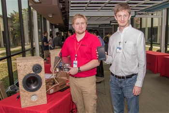
Intern DIY plug-and-play wireless audio system“DIY feeds into our core culture,” said Kasey Arceri, intern program manager. “We as a company embrace innovation and creativity. We want to encourage employees to be makers, not only in their day-to-day jobs, but also outside their jobs.

“We want to encourage interns to embrace that do-it-yourself, maker spirit that keeps innovation going.”

The intern projects ranged from a haptics-enabled cane that could be used by people who have trouble seeing to a convenient system for locking and unlocking doors remotely. All of the projects were based on our microcontroller-based TI LaunchPad™ development kits, Sitara™ processor-powered BeagleBone, and SimpleLink™ wireless connectivity SensorTags.

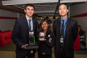
 Intern DIY remote door lock/unlockTeams of business-unit judges selected three winners based on originality, quality, functionality and complexity. A fourth project was selected by votes submitted by TIers on the day of the exhibition. Winners were:

  • LaunchPad kit top design: Blind Spot Detector, which uses haptic feedback to alert drivers when an automobile is in their car’s blind spot as they change lanes.
  • BeagleBone top design: Hi-Fi Wi-Fi Speaker System, which is a plug-and-play wireless audio system.
  • Leadership’s Choice top design: Sonic Technology Integrated Cane (STIC), which provides a vibration to warn visually impaired people when there’s an object close to them.
  • Popular design: Hodor, a convenient, easy way to lock or unlock doors remotely.

Intern DIY haptics-enabled cane“The DIY project catered to the entrepreneurial spirit of a lot of interns,” said Jay, an intern from the University of Michigan at Ann Arbor who was part of the Hodor team. “It’s a great opportunity to build up our technical skills while following one of our dreams. It was a great experience working with great teammates, and it was fun to showcase our project.”

We hired about 550 interns in the United States this summer. About 50 students on 16 teams completed projects for the DIY event.

“DIY with TI is a chance to innovate and learn,” said Angelo, an intern from Arizona State University who was on the team that created the haptics-enabled cane. “This gave us a chance to use TI parts in a whole different way, use our creativity and imagination, make something, and then present it to TI. It’s a rewarding experience.”

Creating DIY projects also helps students stand out when applying for jobs, said Franklin Cooper, a kernel developer in our Software Development Organization who provided direction for interns using the BeagleBone platform.

“When college students go to a career fair, they’re competing for jobs,” Franklin said. “All the students tend to have about the same grade-point averages. They take the same classes and do similar class projects. One of the ways for them to stand out is to develop their own projects. It shows that they’re passionate and willing to work on their own time to create something innovative.”


Smart buildings get smarter with ultra-low-power MCUs

$
0
0
How did everything get so smart? Within building automation systems you’ll find smart thermostats , smart light switches, smart light bulbs, smart refrigerators and heaters and appliances and all manner of smart devices. Add it all up and you’ve...(read more)

Power naps: saving energy using ultrasonic sensing

$
0
0

Doesn’t it feel awesome when you walk into a room and the lights turn on by themselves? It’s likely that the person paying the electric bill feels so too: occupancy sensors correlate with saving energy, which often means saving money. This is typically a high priority for homeowners and businesses alike.

So how do occupancy sensors work? What technologies are used? One common option on the market today is ultrasound – especially in places like restrooms, where a wall might block the sensor’s line of sight. Ultrasonic sensing is similar to radar, but uses ultrasonic waves instead of radio waves. See Figure 1 below.

Figure 1: Ultrasonic wave reflection

Popular ultrasonic-sensing applications include tank-level sensing, drone landing assist and advanced driver-assistance systems (ADAS). As the market for occupancy sensors grows, the potential for additional uses seems limitless. Take the following scenario as an example.

Studying at a university entails walking about 200-300 miles a day – or at least that’s what it feels like. Most students trekking through campus overlook commonplace appliances such as ATMs or vending machines along the path. But there’s one vending machine at UT Dallas that catches my eye every time, probably because it has a large touch screen. Haven’t seen one? They usually look something like Figure 2.

Figure 2: Touch screen vending machine

Before I started working at TI, this vending machine just sat in the “wow, that’s cool!” part of my brain. Now, as an intern working with the PGA450-Q1 ultrasonic sensing signal conditioner, I happened to recall this interactive vending machine and began thinking, “We can make this machine even better.” What I realized is that although fun to look at, vending machines like this consume a significant amount of energy because their touch screens are always on. How do we fix that?

It is possible to use ultrasonic sensing to “wake up” appliances like vending machines and ATMs; the appliance wakes up if someone crosses a certain distance threshold. Otherwise it is asleep, taking a well-needed “power nap.” You could argue that this might not be as beneficial as intended because the appliance will wake up anytime someone walks by. However, think of all the times that no one is close by. That time translates to saved energy, meaning saved money for the appliance owner.

To turn this idea into reality, think about the PGA450-Q1 that I mentioned earlier. A sensing module that uses this integrated circuit can be created to match the needs of a vending machine, ATM or any similar appliance. See Figure 3 for an illustration of how these systems work.

Figure 3: Simplified block diagram

Additional resources

Accuracy? Resolution? Arc minutes? How to take charge of your motor control design

$
0
0

Imagine your commute this morning in your car. The traffic light turned green, and you pushed the accelerator as soon as you could. Your car responded within seconds and you continued on toward the office. But behind the scenes, inside your car, there was a lot more happening. Let’s take a look.

When you press the pedal, the motor does its best to provide the necessary torque to your car through the shafts. The traction motor drives your vehicle forward. This motor (typically a three-phase synchronous motor) is controlled by complex circuitry that consists of several transistors, as well as motor driver, protection and feedback control. The feedback control signal comes from motor position sensors (see Figure 1). These sensors give an analog angle output signal (remember, all real-world signals are analog). This continuous analog signal is converted into the digital domain with the help of an analog-to-digital converter (ADC). Ideally, you could break the continuous analog signal into an infinite number of digital steps, but in the real world, the quantization of an analog signal by the ADC happens in a finite number of steps leading to an error, known as quantization error. Here is where the terms “accuracy” and “resolution” kick in.

Figure 1: Typical system block diagram of a motor-control system in a vehicle

Accuracy

Take as an example a 12-bit resolver-to-digital converter (RDC). Over one revolution of a shaft, the output of the converter has 212 = 4,096 digital codes. In the motor-control world, step size is usually defined in terms of arc minutes or arc seconds. There are 60 minutes in one degree and 360 degrees in one revolution. Thus, over a circle, you have 360 × 60 = 21,600 arc minutes. Since there are 4,096 digital codes, each division is spaced by = 21,600/4,096; that’s 5.27 arc minutes. 5.27 arc minutes corresponds to one least significant bit, or 1LSB. Thus, even when the input angle (a continuous signal) is 100% accurate, the output digital code cannot move by more than 1LSB (or 5.27 arc minutes) before the next code. The RDC specifies this accuracy number by taking into account offset, gain and linearity errors. For reference, the typical accuracy specification for a brushless resolver is 10 arc minutes. The typical error for the entire resolver system, adding the sensor and the conversion error, is approximately ±15.273 arc minutes (10 arc minutes for the resolver sensor and +5.273 arc minutes in my example). These numbers will help us select the appropriate sensor solution for the system, which are typically constrained by these specifications.

Resolution

So, what does resolution mean? “12-bit” resolution means 212 distinct output codes over a 360-degree angular rotation. The actual resolution is simply the number of bits available at the output of the RDC; note that not all of these bits are noise-free. The effective resolution refers to the true “useful” bits from an analog-to-digital conversion, taking into account the signal noise. These are the effective number of bits (ENOB). ENOB is often confused with the resolution stated in the product data sheet.

What does 1 LSB mean?

So far, we’ve reviewed what accuracy and resolution means. Now, let’s take this knowledge and apply it to a system where accuracy and resolution are usually specified in terms of LSBs. Are you wondering how to make sense of an LSB from a systems context? First, let’s look into what 1 LSB translates to in the motor control world, relating to arc minutes and degrees. Here are two examples, 12-bit and 10-bit:

In the 12-bit world, 1 LSB equates to:

1LSB = 360 ÷ 212 = 0.087 degrees = 5.27 arc minutes = ±2.64 arc minutes = ±0.04395 degrees

Similarly, in the 10-bit world, 1 LSB equates to:

1LSB = 360 ÷ 210 = 0.351 degrees = 21.09 arc minutes = ±10.54 arc minutes = ±0.1757 degrees

Conclusion

Isn’t it exciting to see what happens behind the scenes in your car? Accuracy and resolution are the fundamentals of selecting the appropriate sensing solution for your specifications. When accuracy is better than resolution, the converter’s transfer function is precisely controlled over the number of bits of resolution.

Leave a comment below or visit the TI E2E™ Community Automotive forum to join others talking about rotary position sensing.

Additional resources

How to shift your automotive design to another level

$
0
0

Temperature, pressure, radar, cameras, ultrasonics – these are just a few of the sensors used in modern automobiles. Inside the car, you’ll find other complicated systems such as audio, video, gauges and the control unit. Every year more and more systems are added to our vehicles, and many of them need to communicate to work properly. There are times when they don’t exactly speak the same language, however, so a translator is required.

In the world of analog logic, “not the same language” translates to “different maximum voltages.” There are a number of ways you can get systems operating at different logic voltage levels to talk. However, many of them require an extra bit to control direction, or they only operate in one direction. The LSF0108-Q1 is an automotive-qualified bidirectional translator that can operate over a wide variety of voltages without the need for a direction pin. In this post, I’ll discuss the requirements involved with using the LSF0108-Q1 to translate three separate hypothetical signal buses: an I2C bus, secure digital (SD) card and custom field-programmable gate array (FPGA). Figure 1 is a graphical representation of the final circuit.

Figure 1: Schematic diagram for using the LSF0108-Q1 to translate three separate buses; because of the push-pull outputs and low-input leakage currents, pull-up resistors are only located on the high side of each channel

The first pair of signals is for the low-speed I2C bus, converted from the system’s 2.5V primary voltage to the device’s 5V logic level. The next four wires are for the SD card, converting from 2.5V to 3.3V at a much higher speed of 50MHz, which requires a lower pull-up resistance than the other channels (maximum 400Ω). The last two wires are for down-translation from a different controller on the same board operating at 3.3V to 1.8V for the FPGA. The pull-up resistors are all placed on the high side of the translator for each channel. I chose values based on load capacitance and desired frequency ().

Table 1 summarizes this information. For more on how I did this, see the application note, “Voltage-Level Translation With the LSF Family.”


Table 1 – Summary of signals to be translated

The LSF0108-Q1 is capable of translating multiple voltages because it uses a passive translation system, which basically acts like a voltage-controlled switch. When the input voltage is below a certain threshold voltage, the switch is closed and the output is driven low by the input device. When the input voltage is above the threshold voltage, the switch is open and the output is in a high impedance state. At that point, a pull-up resistor takes over and drives the output line to the desired voltage. The VrefA, VrefB and EN pins on the device control the threshold voltage. Figure 2 shows the current flow in different switch states.

Figure 2: Simplified functionality of the LSF0108-Q1: red arrows illustrate current flow when an input is high; blue arrows illustrate current flow when an input is low

Today I showed how to use the LSF0108-Q1 to translate signals for three separate busses that all needed different translation voltages – something that would usually require at least three different parts. I also broke down the operation of the device to a very simple level because I know it can be confusing even to those that have used it before.

Given the large number of systems that have to work together in modern vehicles, voltage translation is an integral building block to get devices talking to one another. Whether it is controllers or peripheral systems that need to communicate, the LSF0108-Q1 will help you shift your logic levels to where they should be. What’s your experience designing with bidirectional translators? Login and leave a comment below.

Additional resources

Why you can't overlook Wi-Fi: It's the connectivity that's here to stay

$
0
0

 Look around you. No matter where you are – whether at home, work or in public – almost every device is “wireless“ and there’s no doubt Wi-Fi® technology is a fundamental enabler. Consumers now understand that Wi-Fi technology is making their lives even better and connecting them to thousands of Internet-based products, such as speakers, thermostats, vacuum cleaners and more.

Think about it! Wi-Fi is a technology that makes all connections seamless. Wi-Fi is the connectivity of choice for millions of existing devices, and also for newer connected products in audio, industrial, building automation and medical applications. Wonder why?

Here are the top four reasons:

  • Ease of integration: There is a broad existing infrastructure for Wi-Fi. Most homes, industrial settings and commercial areas already have an existing Wi-Fi network, if not multiple.
  • Security: Wi-Fi has industry-standard security features that consumers can rely on to help protect their data. A Wi-Fi network can provide both security and privacy for data communication as it travels across your network. TI’s single-chip security solutions help developers protect their intellectual property (IP), as well as their users’ data, and identities.
  • Low-power systems: TI’s cutting-edge power optimization techniques allow battery-powered applications to run for multiple years.
  • Great connectivity range: Wi-Fi connectivity can run up to a few kilometers, with cloud connectivity enabling communication for even more kilometers beyond that! This allows users to remotely monitor their systems and “things” from any Wi-Fi-enabled device like smartphones or tablets.

Knowing what you do about Wi-Fi technology, did you know Texas instruments has been a leader in embedded Wi-Fi for more than a decade? In addition, did you know TI has shipped millions of units worldwide? TI has exhibited supplyconsistency and stability and is a preferred supplier for hundreds of Wi-Fi customers across a wide variety of applications.

With the Wi-Fi market being so dynamic, customers are looking for an easy-to-use, out-of-the-box solution that can provide the best user experience and is available without supply disruptions for a long period.

Here’s why you need to pick a Texas Instruments Wi-Fi solution for your next design:

  • Longevity of supplyand support with a 10-15 year lifecycle
    • Access to TI's worldwide sales and applications teams to support development
  • Flexibility of offerings depending on the customer and application requirements
  • Certification takes the guess work out of your design

A strong ecosystem makes is easy to start development and gets you to market faster

  • Easily available content such as app notes, software downloads and more helps you avoid common design challenges. Lean more at www.ti.com/wilink and www.ti.com/simplelinkwifi
  • Software support
  • Bundle options with other TI microcontrollers (MCUs) or microprocessors.
  • Strong partner network for customized solutions

Start learning more about TI’s Wi-Fi solutions today! www.ti.com/wilink and www.ti.com/simplelinkwifi.

Inductive sensing: WEBENCH® Coil Designer now designs stacked coils for switch applications

$
0
0

In my last post, I showed step by step how WEBENCH® Coil Designer can produce the sensor computer-aided design (CAD) files for inductive-sensing applications. This method works well for single-coil inductive sensors such as the LDC1614, but the LDC0851 inductive switch requires two sensors, which can either be side by side or stacked.

With the most recent WEBENCH updates, it is no longer necessary to draw coils by hand; WEBENCH Coil Designer produces coil designs in less than five minutes. Today, I will show you how to design stacked coils in the WEBENCH tool.

What is the difference between stacked and side-by-side coils?

A side-by-side arrangement, as shown in Figure 1, enables the greatest sensitivity and is easily implemented for a two-layer printed circuit board (PCB). Exporting two identical coils from the WEBENCH tool and connecting them on one PCB is a sufficient side-by-side coil implementation.

An alternative arrangement is the stacked-coil arrangement, in which the coils are stacked on top of each other on a four-layer PCB. Placing the sense coil on top ensures that the influence of the target on the sense-coil inductance is always stronger than on the reference-coil inductance. This approach is commonly used for space-constrained proximity-sensing applications such as door open/close detection.

Figure 1: Side-by-side coil arrangement (left) vs. stacked coil arrangement (right)

How do I use WEBENCH Coil Designer to design stacked coils?

To design a stacked coil with WEBENCH Coil Designer, follow the five steps shown in Figure 2.

Figure 2: Five steps for designing a stacked coil in WEBENCH Coil Designer

You can export the coil to any of these CAD formats:

  • Altium Designer.
  • Cadence Allegro 16.0-16.6.
  • CadSoft EAGLE PCB (v6.4 or newer).
  • DesignSpark PCB.
  • Mentor Graphics PADS PCB.

I used the default settings, which represent the coil on the LDC0851 evaluation module. This configuration is particularly good for sensing larger targets. Note that if you are sensing the presence of small targets such as a screw head, you should add more turns so that the coil-fill ratio (dIN/dOUT) is less than 0.3.

Figure 3 shows the layout in Altium Designer. The Top Layer and MidLayer1 contain the sense coil, while the reference coil spans from MidLayer2 to the Bottom Layer.

Figure 3: The finished coil in Altium Designer format

Where is the switching point?

The maximum switching point scales with the coil diameter. You can reduce the switching point down with the ADJ pin to fine-tune the switching distance. For stacked coils, put the LDC0851 in threshold adjust mode. Figure 4 shows the switch-on and switch-off points for a 20mm stacked coil that I designed. The maximum switching distance is about 6.8mm for an ADJ setting of 1 and is scalable down to about 1.2mm for an ADJ setting of 15.

Figure 4: Threshold set and release points


Designing stacked coils for inductive-switch applications doesn’t need to take much time. By following the approach I’ve described in this post, you can design a coil and export it to the PCB CAD tool of your choice in less than five minutes.

Do you find our WEBENCH tools for inductive sensing useful? Are there other WEBENCH tool features that would make your system design with LDCs easier? If so, leave a note in the comments section below.

Additional resources

How to save power while shrinking your next mobile design

$
0
0


Where did my charger go?  My laptop is running low on battery again as I’m typing this.  We are constantly struggling with battery life in today’s always-on connected world.  Everything we use needs a longer battery life, but also needs a smaller battery.  Impossible you say?  Certainly not, but this trend of shrinking form factor while extending battery life poses a serious challenge for many of today’s circuit designers.

Why can’t I use a smaller battery to make my product smaller?

The largest component of almost every portable product is the battery itself, second only to the screen.  Thus, the easiest way to reduce the form factor of these products is to reduce the battery.  Problem solved!  Right?  Not so fast…by reducing the size of the battery, you are also reducing the capacity of that battery, meaning a smaller battery not hold as much charge as a larger battery will.  This means that you must be more efficient in your power consumption in order to obtain the same lifetime.

How can I be more efficient with my power consumption?

There are two main ways we can extend battery life.  The first is by reducing our active power consumption.  This is done by minimizing the amount of power drawn when you are talking on your smartphone or checking your Facebook news feed.  This can be accomplished by investing in a more efficient processor or more efficient DC/DC converters which consume less quiescent (active) current.  It could also be improved by obtaining a more efficient screen and backlight, or by simply using the device less often (but that’s no fun at all).  The second method to extend battery life is to minimize your power draw when in “standby” or sleep mode.  This is frequently referred to as shutdown current.

Let’s reduce our standby power consumption

One popular method of reducing standby power consumption is through the use of load switches.  A load switch can be used to disconnect power-hungry components from the battery when not in use.  By doing so, you can lower your standby power consumption and extend battery life.  This approach was used to maximize the battery life of our mPOS (Mobile Point of Sale) Power Reference Design.  By connecting the TPS22918 load switch to loads such as the WiFi, Bluetooth and GPRS radios, as well as the LCD screen, we are able to ensure that customers could use their mPOS all day on a single charge.  And when it does come time to recharge, the design also features 15W USB Type-C charging made possible by the TUSB320 and bq25890 battery charger, which dramatically reduces the recharging time.

How does USB Type-C help recharge my battery faster?
By implementing USB Type-C charging on your next design, you are able to charge at a higher wattage than previously possible.  Typical USB chargers today charge at either 2.5W (5V 500mA) or 5W (5V 1000mA), but USB Type-C supports up to 100W (20V 5A) charging!  This dramatically reduces the amount of time that battery powered devices need to remain tethered.

Next time you are faced with the challenge of designing smaller but still needing a long battery life, don’t forget about TI’s broad portfolio, with everything from highly efficient and compact DC/DCs, to battery chargers, USB Type C solutions, and even load switches, TI has the solutions you need to power up your next design. Kick start your design now and download the  mPOS (Mobile Point of Sale) Power Reference Design!

Additional resources


When green meets the IoT

$
0
0

When it comes to lowering the rate of power consumption wherever possible, two seemingly unrelated trends – the Internet of Things (IoT) and the green power movement – seemingly converge. Of course, low-power consumption is nothing new for designers of embedded systems. The two trends do add to the pressure already felt by designers to develop systems that not only consume less power themselves, but also help reduce the power consumption of other systems so that the overall rate of power consumption decreases. 

To ease the pressure on embedded system designers, several new microcontrollers (MCU) such as TI’s MSP430FR2311 MCU are being integrated with all of the building blocks needed to be a low-power power monitoring system. A very versatile analog front end comprised of several standard operational amplifiers and what is rarely found included on a MCU, a super-sensitive low-current transimpedance amplifier (TIA), are integrated with an analog-to-digital converter (ADC), highly configurable ferroelectric random access memory (FRAM), and even an oscillator to provide a flexible platform for a wide variety of power monitoring applications.

Small embedded devices with power monitoring requirements are already popping all over the IoT. Just one example is the wireless switches which control a light in a room, a bank of lights in an office or a large industrial space. Such switches must consume little power on their own, since some will be battery operated. And in addition to turning light fixtures on and off, some wireless switches will be asked to keep track of the power consumed by the lights scaling back the power or example, for the lights to stay within a certain power budget, or in combination with a motion sensor or turning off the lights entirely when the space is unoccupied. The permutations are practically endless.

A highly integrated MCU consumes less power and has reduced space requirements, making its embedding into a small light switch that much easier while also reducing the bill of materials (BOM) costs by eliminating discrete devices from the design. With on-chip op amplifiers, an ADC and a digital processor, the MCU can monitor an analog current, convert this into a digital signal and process it all inside one device. Plus, an integrated crystal lowers the MCU’s standby power consumption to as low as 170 microAmps while maintaining a speedy wake-up response of less than 10 microseconds. And, with one block of FRAM instead of the typical combination of RAM and Flash, designers have the flexibility to decide how much storage space to allocate to code and how much to data logging. The designer decides, not the resources on the MCU.

A major emphasis of the green movement is power consumption ratings like the U.S. government’s Energy Star ratings, which are prominently associated with all sort of appliances and office machines such as ink jet and laser printers. A highly integrated power monitoring MCU could act as a housekeeping processor over the power subsystem in a larger system, such as a printer, for example, to ensure a favorable power consumption rating. A low-power MCU would not consume much power on its own and it could monitor the current flowing into the printer. When the printer is not in use, the power-monitoring MCU would notify the system’s main microprocessor, which could either gradually shut down nonessential sections of the system or just shut down the system entirely to reduce power consumption.

Since they deliver the performance and capabilities prized by a wide range of market segments and meet the needs of the major trends that are driving marketplace demand, MCUs like the MSP430FR2311 MCU will be a good fit for many applications for years to come.

Follow along with our other blog posts related to MSP430FR2311 MCUs:

Eight things to consider when choosing haptic feedback – part 2

$
0
0

In the first installment of this two-part series, I discussed five things you should consider when picking a haptic driver and recent haptic advancements. To close this series off, we will cover the three remaining reasons.

Closed-loop architecture

As in most systems, closed-loop architectures are the most ideal designs. TI’s closed-loop architecture provides several benefits for driving linear resonance actuators (LRAs) and eccentric rotating masses (ERMs).

ERMs are driven at DC voltage levels, so the resonance-tracking portion of the algorithm is not necessary. Instead, the DRV262x family takes advantage of other properties of the DC motor – mainly the attribute called back electromotive force (EMF). When an ERM is off, the motor produces current that is fed back to the outputs of the DRV262x. This current is used to determine how strong to push the motor for the next cycle. By measuring the back EMF, the DRV262x family reduces the power consumption needed to drive an ERM. Essentially, the TI haptic driver takes advantage of the momentum of the rotating mass and only provides the necessary push to keep the motor’s acceleration constant. This feature leads to power savings when compared to a discrete field effect transistor (FET) solutions.

As you may know, LRAs are high Q systems, meaning that they operate efficiently at a specific frequency. Figure 1 depicts the typical operating frequency of an LRA. Operating an LRA at a frequency just 2.5Hz outside of the resonance frequency can result in a 40% loss of acceleration. TI’s algorithm uses the properties of these LRAs to ensure that the drive frequency is within 2Hz of the actuator’s resonance frequency. The DRV262x can also accommodate a wide range of LRA frequencies from 45Hz to 300Hz. Just like the ERM, the back EMF is used to make sure we drive the LRA to its maximum potential with minimal effort. 

Figure 1: LRA high Q system

Power consumption

This next feature is arguably the most important feature of the DRV262x family: in shutdown mode, the driver consumes only 105nA. Power consumption for personal electronics, wearables and infotainment consoles is trending downward with technological advancements. Battery capacity continues to grow, but designers need to tackle power consumption from both sides. Since designers are trying to run haptic devices on less power, the TI haptic team is focusing on ultra-low power devices, such as the DRV2624 and DRV2625, which improves power consumption from the previous haptic driver by 10x.

One issue with keeping parts in shutdown mode is the wake-up time. For haptics, it is especially important to provide a fast response time. With the DRV262x haptic driver, users can wake up the part and implement a waveform in 1ms, making the response time miniscule.

Integrated haptics library

On a different note, some may not know where to start with haptic feedback; others may know exactly what they want. For those who aren’t sure where to start or are looking for a simple haptic implementation, the DRV2625 ships with a licensed implementation of Immersion’s TouchSense 2200 waveform library. This library contains 123 waveforms that can provide effects from single clicks to ramp-transition clicks for gaming applications or custom haptic feedback alerts. The DRV2625 has the option to implement as many as eight waveforms in a single sequence, and those sequences can be looped in numerous ways to create endless configurations.

For those with haptic experience who want to create custom effects, the DRV2624 ships with 2kB of programmable RAM to create custom effects geared toward video games, virtual reality or other applications. Using a microcontroller, products can have numerous haptic effects stored in a central library and loaded into RAM based on user experiences. This makes the DRV2624 extremely versatile.

Bonus: controlling your driver

 The future of integrated electronics will be heavily impacted by the ability to engage customers through the sense of touch. When looking for a place to start with the aforementioned drivers, consider using evaluation modules (EVMs), such as the DRV2625EVM-CT and DRV2624EVM-CT in conjunction with haptic control console (HCC). HCC is a program designed to make using haptic EVMs easy by utilizing an on board MSP430. This software controls every aspect of the DRV262x driver.

Now that you know what to look for when selecting a haptic driver, you should now be able to evaluate the different options and decide what is right for you. The haptic features for an automobile will be different than haptics in a smart watch or mobile device. There are certain features you should be on the lookout for, however.

Let me know what you think of these eight considerations. Would you add others?

Additional resources

Bionic arms turn kids without limbs into superheroes

$
0
0

For kids who dream of being a superhero or heroine, receiving a bionic prosthetic arm that looks like something out of Iron Man or Captain America might be the highlight of their young lives.

Alex PringIt’s right up there with overcoming a disability that once kept them from riding bikes, playing video games and all the other things kids enjoy doing.

With a little help from TI, students at the University of Central Florida (UCF) are making dreams a reality for children who were born without an arm or who have lost an arm.

One of those kids is Alex Pring, an 8-year-old Iron Man fan who was born with a partially developed right arm.

“Alex was very shy before – even afraid to go into a grocery because of how people would treat him or because they would ask questions that would hurt his feelings,” said Albert Manero, executive director of a nonprofit group called
Limbitless Solutions. “Now he’s probably the most confident 8-year old you could imagine.

“He is very confident of his prosthetic arm.”

But this is not just any prosthetic arm. It’s a personalized, custom-made arm with movable hands and fingers, and all of its parts were printed on a 3-D printer. Alex’s arm looks just like the arm Iron Man uses to make the world safer.

He calls his prosthetic arm “the best gift ever.”
Click here to watch a video of Alex receiving his arm from Iron Man actor Robert Downey Jr.

“We thought kids just wanted to blend in and feel normal. But we found out it’s more about personal identity and expression,” Albert said. “It’s not a defect for them; it’s a facet of their personality.”

The TI-Limbitless connection

Prosthetic arms typically start around $40,000 – a pricetag that most people cannot afford even through insurance. Limbitless has built about 20 arms for children at no cost to their families. The idea is to show recipients that there are no limits.

“No one should profit at the expense of a child that was born without an arm,” Albert said. “We are finding innovative ways to make the arms more cost-effective so we can continue doing this.”

When Limbitless first started its mission two years ago, the arms cost around $350 in materials, including plastics, hardware, batteries and motors. We have helped the group reduce its materials costs by about 15 percent by providing a fully integrated board of TI analog, MCU and connectivity devices. The board has also helped increase the arm’s functionality.

“We are constantly innovating and improving,” Albert said. “Using TI chips has extended the performance and battery life of the system because the chips are more specialized for what we are trying to do. It’s a big leap forward.”

The arm and hand operate with the help of three electrodes attached to the user’s arm muscles. When the user squeezes a muscle, an electrical pulse triggers the Servo motor to open or close the hand. Engineers hope to increase the functionality of the arm even more in the future.

UCF grad Carolus Andrews has been researching ways to incorporate haptic feedback and Bluetooth into the arms.       

Haptics can help users know if they have a good grip on an object. The gentle buzzing of the haptics also reminds them to set objects down to avoid draining the battery. The arm drains power faster when the arm's Servo motor is engaged and the hand is closed on an object, Carolus explained.

“Alex asked if we could include haptics in the arm we were building for him,” he said. “We thought it was a great idea.”

Carolus recently joined TI as an applications engineer through our apps rotation program, but he still does volunteer work for Limbitless.

Back on the UCF campus, the Limbitless team produces the arms on 3-D printers inside the TI Innovation Lab. We have supported the students there by providing them test boards and evaluation modules to work with and giving them access to senior designers that they can call with questions.

Peter Balyta, president of our Ed Tech business, describes the TI Innovation Lab at UCF as a maker space where students across multiple disciplines can turn their ideas into prototypes.

Cheerleader“TI is bringing real-world engineering concepts to life for thousands of students in these labs worldwide,” said Peter, who leads all academic engagements for TI, including our university marketing program. “And, what’s more, we’re also showing how students are taking those concepts and creating functional, working designs that are truly improving people’s lives.”

The Limbitless team also is using the Innovation Lab to build a patent-pending bionic wheelchair that a user can control with his or her face muscles. The group worked with a paralyzed war veteran to create the wheelchair.

“A lot of our ideas are coming out of the TI Innovation Lab,” Albert said.

Finding inspiration

 
Albert originally got the idea for the bionic arm while driving his car. He heard a story on the radio about a man in Washington State who developed the first 3-D-printed mechanical hand for a carpenter in South Africa.

“I went to my research lab and said, ‘I have to be a part of this. What can I do to help?’” Albert said. “Then Alex’s parents contacted us and asked if we could build their son an arm.”

Since then, the group has produced and delivered about 20 robotic arms to children. About 480 kids from 50 countries are on a waiting list for arms. Limbitless plans to help hundreds of kids in the next year and eventually thousands of kids.

The robotic arm has been a fulfilling project for Albert, who credits a great team of 80 volunteer students from various backgrounds.

“It’s exciting to take what you are learning in academics and help someone. It’s the most rewarding work you can do. When you see the smiles when you’re able to deliver an arm, it makes it all worth it,” said Albert, a Fulbright Scholar who is currently getting his Ph.D. in mechanical engineering from UCF.

“We’re going to make a lot of superheroes.”

If you would like to learn more about how Limbitless is helping children, go to the group’s
Website.
 

Photos courtesy of KT Crabb Photography.

Engineering magic: Touch through thick glass to control LEDs and LCD

$
0
0
Not impressed with the magic trick revealed in the previous post ? Then check out this one: We kept working on our touch-through-glass application and managed to improve it. Using an MSP430™ microcontroller (MCU) with CapTIvate™ technology...(read more)

How to design cost-sensitive DC instrumentation circuits

$
0
0

Many sensors produce low-level DC outputs that require a high input-impedance amplification stage to increase the signal amplitude. Sensors used in personal and portable electronics require operational amplifier (op amp) circuits that provide high input impedance and DC precision, while also being low power and cost-effective.

In this post, I’ll explain how to design a few cost-optimized low-power DC-accurate circuits using TLVx333 op amps in different circuit configurations. These devices provide high levels of DC accuracy with maximum input offset voltages (VOS) less than 15µV, and a typical VOS drift of 0.02µV/°C. The 0.1Hz to 10Hz low-frequency noise specification is only 1.1µVpp and the 0.01 – 1Hz noise specification is only 0.3 µVpp. Table 1 shows the key performance metrics for TLVx333 family.

Table 1: Key specifications for the TLV333

Single-ended sensors can interface with standard noninverting amplifier circuits, as shown in Figure 1. The transfer function is shown in Equation 1. Noninverting op amp circuit-offset errors are dominated by the input offset voltage (VOS) and the VOS temperature drift of the op amp. Additional offset errors come from the CMRR and the input bias current of the op amp. The tolerance and temperature coefficient of the resistors in the feedback network set the gain error and gain-error drift. The circuit shown in Figure 1 is configured for a gain of 500V/V, and the closed-loop bandwidth is 1.14kHz.

Figure 1: TLV333 used in a noninverting amplifier configuration

Sensors with differential outputs such as bridge sensors and strain gauges require a circuit with differential inputs. One of the simplest options to interface with a differential sensor is the four-resistor difference amplifier circuit shown in Figure 2. If R1 is set equal to R3 and R2 is set equal to R4, then the transfer function simplifies to Equation 2. The tolerance of the resistors in the difference amplifier will directly affect the CMRR of the circuit. Selecting 0.1% resistors achieves at least 54dB of CMRR, while 0.01% resistors achieve at least 74dB. Note that discrete difference amplifier designs will typically not match the performance of integrated solutions, but they often offer advantages in flexibility and cost. The circuit in Figure 2 is configured for a gain of 499V/V, with a closed-loop bandwidth of 1.16kHz.

Figure 2: TLV333 used in a difference amplifier configuration

High-impedance sensors with differential outputs often require circuits with input impedances >1MΩ. Achieving input impedances >1MΩ is often not practically possible using a discrete difference amplifier topology. Large resistors will increase the DC errors from input bias current, increase circuit intrinsic noise, increase susceptibility to extrinsic noise and will likely require stability compensation.

Figure 3 shows a discrete two-op-amp instrumentation amplifier (INA) using a dual-channel TLV2333. The two-op-amp INA presents a high-impedance differential input to the sensor while only requiring two op amps and five precision resistors. Assuming that R1 is set equal to R3 and R2 is set equal to R4, Equation 3 shows the transfer function. The circuit in Figure 3 is configured for a gain of 500V/V, with a closed-loop bandwidth of 1.02kHz.

You can also construct a discrete three-op-amp INA using a dual-channel op amp, a single-channel op amp and seven precision resistors. Equation 4 shows the transfer function for the three-op-amp INA. INA designs often require a buffer for a high-impedance reference or an op amp used as an integrator to high-pass filter the input signal. Figure 4 shows a TLV4333 used to create a three-op-amp INA with a reference buffer. The circuit in Figure 4 is configured for a gain of 500V/V and has a closed-loop bandwidth of 1.16kHz.

You can use the TLVx333 family of devices in several ways to create DC-accurate circuits that are ideal for cost-optimized precision-sensor acquisition and precision-instrumentation applications.

Have questions about other op-amp designs? Log in and leave a comment.

Additional resources

Viewing all 4543 articles
Browse latest View live


<script src="https://jsc.adskeeper.com/r/s/rssing.com.1596347.js" async> </script>