Quantcast
Channel: TI E2E support forums
Viewing all 4543 articles
Browse latest View live

It may be small, but it’s powerful

$
0
0

In a world where memory and pin count increase on an almost daily basis, we sometimes hear questions asking why we continue to develop and release microcontrollers (MCUs) with only a few kilobytes (KBs) of memory.  Well the answer is really quite simple. There are hundreds of applications that can benefit by using a low-power MCU to replace standard logic or other analog circuits.  Often these MCU-based solutions provide new functionality and flexibility, bringing additional value to a design.

 As an example, we could connect a temperature sensor to the analog-to-digital converter (ADC) and with a few lines of control code we can build a simple temperature controller. The diagram below shows the system using the LMT88 temperature sensor and a potentiometer to create a simple closed loop on / off control system by switching a relay to control a heating element.  

Figure 1: Block diagram of a simple temperature control system

By changing the temperature sensor to an ultraviolet (UV) sensor we could build a simple UV exposure monitor that measures UV levels over a given time period, or by using a simple moisture sensor we could maintain soil moisture levels by controlling an irrigation system.  While these types of applications can be built with a few simple active and passive components such as a thermistor and a comparator, we can easily add a programmable element into the feature set or enable more advanced control features such as implementing a proportional term controller to control a variable heating element or a variable speed pump.  We can easily enable an interface to allow the user to change the set point or to vary the level of hysteresis, it isn’t always as simple to do with a hard wired analog or fixed function IC based solution.

We have recently released two new MSP430™ MCUs with low pin count that are perfect for many simple applications.  With up to 4 KB of embedded ferroelectric random access memory (FRAM), plus 1 KB of RAM, these devices offer a compiler friendly alternative too many of the 8-bit MCU’s on the market today.  These new low cost MSP430 MCU devices are a great entry point to see what FRAM is all about.  Offering great flexibility for programmers, FRAM’s unique ability to operate as both non-volatile program and non-volatile data memory allows developers to customize the partitioning of program and data memory that was previously not possible with conventional flash and RAM combinations.  Along with this flexibility, FRAM offers significant energy savings when writing to memory compared to EEPROM or flash memory, you can find out more about FRAM technology here.  

The MSP430FR2110 and MSP430FR2111 MCUs pack a significant feature set into a tiny 3x3 mm package.  Besides offering up to 4 KB of embedded ultra-low power FRAM non-volatile program storage, they also include:

  • 10-bit 200K sample ADC with eight external input channels
  • Low-power comparator with a 6-bit programmable threshold
  • Real-time counter with low-power backup memory
  • Hardware UART / SPI serial interface 

With 1K pricing under $0.50 for the MSP430FR2110 MCU,  this cost effective, feature packed device is already finding many new applications, what would you do with it?

To begin development we have the low cost ($15.99) MSP-EXP430FR2311 LaunchPad™ development kit, there is also a 20 pin TSSOP target socket board, MSP-TS430PW20.

How to get started:


How to build a monitor and control solution for voltage regulators

$
0
0

In my last post, I talked about how to use a precision digital-to-analog converter (DAC) to margin a voltage regulator like a low-dropout regulator (LDO) or switch mode power supply (SMPS), providing the ability to either precisely tune the output or allow it to swing over a wide range of voltages.

In this post, I will expand upon that idea to build a closed-loop system that, alongside the compute power of a microprocessor, creates an all-in-one analog monitor and control solution for voltage regulators. Let’s return to the example circuit in Figure 1 that I used last time with an LDO and a DAC.

Figure 1: Voltage regulator margining circuit

The DAC shown controls the regulator circuit by sinking or sourcing current – thereby raising and lowering the voltage output of the LDO. You can add monitoring to the circuit by using a precision analog-to-digital converter (ADC) to sample the voltage at the output of the LDO. Additionally, many regulators have an enable pin that you may want to control as well. You can do this by using a general purpose I/O GPIO from the microcontroller. Figure 2 shows these monitor and control devices in the system surrounding the LDO.

Figure 2: Voltage regulator monitor and control system

What would be very helpful is if you could use one device to accomplish the functions of the DAC, ADC and GPIO. Fortunately, TI has a portfolio of analog monitor and control (AMC) devices that integrate all three of these discrete devices into one product.

Let’s use an example where you need to monitor and control four power supplies. A device like the AMC7891 would be great for this application because it has four DACs and more than four ADC inputs and GPIOs. Figure 3 shows how the AMC7891 fits into this system.

Figure 3: A multiple-rail voltage regulator monitor and control system

The AMC7891’s integration enables you to eliminate many discrete devices from the board and centralize the control of the power supplies to just one device.

Here are a few helpful tips when designing this solution into your system:

  • SMPS outputs are inherently noisy with the voltage ripple from the switch. Take multiple samples of the output voltage with the ADC and average the samples before changing the DAC code to compensate.
  • If your regulator output voltage exceeds the ADC input voltage, you will need to use an external amplifier to add a fractional gain to the output voltage to get the signal within range.
  • Put your ADC trace as close as possible to the downstream devices so that you get the most accurate measurement possible at the point of load.

You can visit ti.com/amc to find more integrated precision ADCs and DACs that are similar to AMC7891. TI provides a very broad portfolio of these devices, many having more inputs and outputs for your control system.

Additional resources

Output inductor considerations in a synchronous buck converter

$
0
0

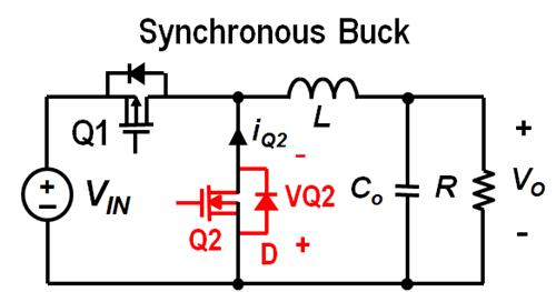
Inductors are an essential component of switching voltage regulators and synchronous buck converters, as shown in Figure 1. In all switching regulators, the output inductor stores energy from the power input source when the MOSFETs switch on and releases the energy to the load (output).

Figure 1: Synchronous buck DC/DC converter

You should select inductors to manage output capacitor size, load transients and output ripple current. There are benefits of both low and high inductance values.

The benefits of low inductance include:

  • Lower DC resistance (DCR), which is inherent in the inductor wire, and which affects ripple and power loss.
  • Higher saturation current, for higher output-current capability.
  • Higher slew rate (di/dt), which improves load transient response and reduces output capacitance for a given load transient.

The benefits of high inductance include:

  • Lower ripple current, which in turn reduces:
    • AC losses (inductor skin effect).
    • MOSFET root-mean-square (RMS) current.
    • Output capacitor RMS current.
    • Output capacitance for an equivalent output ripple.
    • Continuous inductor current over a wider load range.

Equation 1 calculates the output inductor value:

where L is the output inductance, VOUT is the target output voltage, VIN(max) is the maximum input voltage, FS is the buck converter switching frequency and IRIPPLE is the target output ripple current.

I recommend sizing the ripple current for 10% to 30% of full load. Plugging values into Equation 1, Equation 2 shows the output inductance calculation result:

In this case, I selected the PG0077.801 inductor from Pulse Electronics. Table 1 shows its relevant parameters.

Table 1: PG0077.801 inductor parameters (image courtesy of Pulse Electronics)

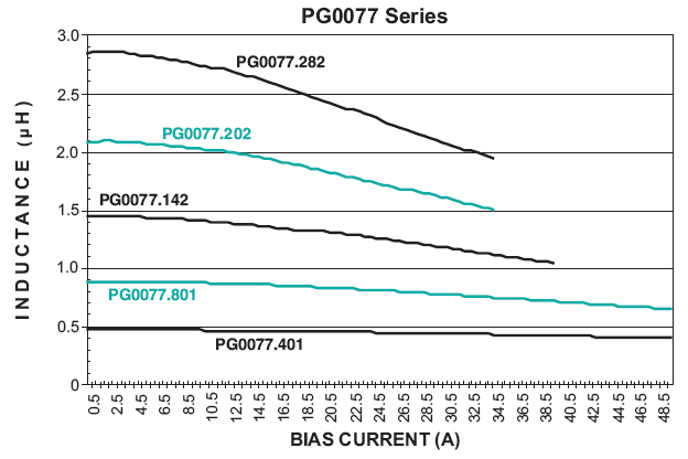
It is important to check the inductance vs. the load (bias) current, as inductance decreases with increasing current. Then you can determine what the actual inductance is at the target load current.

If you assume 15A of continuous output current, the actual inductance is 0.83mH, as shown in Figure 2.

Figure 2: Inductance vs. current (image courtesy of Pulse Electronics)

Once you know the actual inductance value, you can recalculate the ripple and RMS currents. Equation 3 recalculates ripple current:

Equation 4 recalculates RMS current:

You can also calculate the inductor losses. Total inductor losses are winding losses and core losses, expressed by Equations 5 and 6:

where K1 = 13.77 x 10⁻⁹ , K2 = 39.4, FSW = 500kHz, DI = 3.32A (the calculated ripple current) and PCORE = 0.983W.

In this example, the total inductor power loss is 0.294W + 0.983W = 1.277W.

There are many inductor types to choose from, but most buck DC/DC converters typically use ferrite drum and iron powder toroid inductors. So when designing a buck converter, keep these inductor selection criteria in mind for a high-performance, stable and reliable design. Check out TI’s buck converter and buck controller selection tables for a variety of buck DC/DC solutions.

Wireless power during the zombie apocalypse

$
0
0

bq501210 evaluation module (EVM)

Did you know, the Centers for Disease Control and Prevention has a web page from the Office of Public Health Preparedness and Response to address zombie preparedness.  They claim that it is tongue in cheek, but we all know better.

Here’s a horrifying thought, what happens when things go south and the zombies start roaming?  How will I keep my personal electronics (phone, tablet, watch and others) charged?  What if I’m attacked and get zombie brain matter all over my USB connectors?  As part of my zombie apocalypse preparedness measures, I’ve started stocking up on spare rechargeable batteries and buying wireless powered devices whenever I can. 

The Wi-Fi®, LTE and Bluetooth® in my valuable electronics will transfer data through the gore, but, their batteries need to be recharged too.  But, how do I get a decent charge?  That’s where wireless power comes in.  As long as my home base is safe, I can keep my power transfer going.  After wiping away whatever gets on my phone I can place it on the charging pad and get a full recharge.

I’ve even taken the liberty of modifying some of my important electronics to add wireless power.  Monitoring my healthy activities can’t stop just because of a zombie or two.  I’ll need to keep my fitness tracker running.  Gotta keep that heart rate monitored.  And what about playing a game or two on my favorite app?  What does wireless power have to do with this?  I’ve seen enough of the movies to know things can get very messy. I need the Bluetooth® speaker to either broadcast my personal theme song, or find out what tunes drive the zombies mad.  Yes, I’ve thought about this a lot.

While I prefer to buy the devices with wireless power built in, there are after-market products that supply wireless power.  I also create my own wireless powered electronics.  I start with the receiver portion, where   I have several good choices.  TI’s bq51222 is a great multipurpose solution.  It’s fully certified to the latest Wireless Power Consortium (WPC) v1.2 and Power Matters Alliance (PMA) standards.  With the adjustable output voltage feature, I simply adjust the output to the desired voltage (generally 5V for USB, but you can set it up to 8V).  To keep the USB option available after I add wireless power, I add a simple dual FET like the CSD75207W15 NexFET™ power MOSFET between the USB input supply and the bq51222 output.  This prevents any power contention if I’ve got both USB power and wireless power active at the same time.

Other options include the bq51013B (another 5W solution) or the bq51003 for the smaller wearables requiring less than 2.5W.  For higher powered solutions (tablets and some fast-charging phones), I like the bq51025 since it is fully Qi-certified at 5W and can also deliver 10W when paired with the right transmitter.

Speaking of transmitters, for the 5W, I like the bq500511A and bq50002A two-chip solution due to its small BOM count.  The newly released bq501210 15W transmitter is WPC v1.2 certified. .  It works with all 5W Qi-certified receivers, will get that 10W out of the bq51025 and can deliver 15W with the right receivers.  There are several TI Designs that can help you on the wireless power learning curve.  The E2E™ Community Battery Management forum is a great way to get detailed design help from experts on TI’s entire product portfolio.

Last, but not least, if you’d like to hear about how to get your batteries fully charged in the quickest time and how to make sure your battery powered taser has full capacity, let me know in the comments below.

Additional resources:


How an eFuse can help provide robust industrial power path protection

$
0
0

Any electronic systems are often subjected to harsh environments and threats such as electrostatic discharge (ESD), electrical fast transient (EFT) and lightning surges. Power designers must prioritize circuit protection to prevent system failure, especially for industrial applications with a 24V supply rail. 

Circuit protection schemes are capable of protecting the power supply and the overall system from events such as overcurrent, short circuit, input inrush current, overvoltage, undervoltage, input reverse polarity protection (commonly known as miswiring) and reverse current blocking.

In this blog I will give an overview of several approaches to robust industrial power path protection including discrete implementation, hot-swap plus ORing controller approach and integrated implementation.

Discrete implementation

Figure 1: Discrete protection scheme

Discrete implementation schemes are the most traditional way of power path protection using a protection scheme in the power path one example is shown in Figure 1.

A discrete implementation utlizes a power diode in series to protect the system from reverse polarity (miswiring) and reverse current. If a circuit draws 2A of current, it dissipates ~1W of power across the diode, which will increase the board temperature. Resonant circuit (L-C) filters and multiple TVS diodes control the input line transients during surge test (International Electrotechnical Commission (IEC) 61000-4-5).

The implementation utilizes a PFET (high-side switch) along with bi-polar junction transistor BJTs, operational amplifiers, Zener diodes, resistors and capacitors to fulfill all protection requirements. This system solution is bulky and has a larger bill of materials (BOM) count. Additionally, this implementation does not address thermal shutdown protection and current-limit accuracy variations with temperature.

By utilizing a traditional fuse, a discrete implementation protects against short-circuit events. The fuse takes milliseconds to seconds to break during short circuit, which can damage the load. Be sure to check out my colleague’s blog for more information on upgrading your fuse.

Hot-swap plus ORing controller approach

Figure 2: Controller + MOSFET protection scheme

Another common approach, as shown in Figure 2, to power protection is through a hot-swap controller and an ORing controller. This scheme uses external FETs to make the design more efficient and reliable. Unfortunately, this implementation still has challenges, such as controlling external FETs, external sense resistance and implementing an additional circuit for input reverse-polarity protection. This implementation struggles to manage thermal and safe operating area (SOA) protections due to the external FET architecture. Even though this solution is better than a discrete implementation, it is not suitable for space-constrained systems such as input/output (I/O) modules.

Integrated implementation (eFuse)

Figure 3: Integrated protection scheme

On the other hand, imagine that your entire discrete implementation vanishes into a single integrated device, barring a few components like Transient Voltage Suppressor (TVS) diodes, resistors and capacitors, as shown in Figure 3. That would be really cool, right? An eFuse typically integrates all of the protection features mentioned above into single device, efficiently and with minimal design efforts.  EFuses also incorporate features like voltage, current monitoring and fault indication for system diagnosis – apart from power path protection.

The SOA protection of FETs and robust thermal protection ensures the protection of the eFuse, as well as the load in harsh environments. It is also suitable for space-constrained applications, as integration helps reduce the system solution by more than half.

One of these types of solutions is the TPS2660, the industry’s first 60V back-to-back FET integrated eFuse. The device is definitely worth considering for your new designs as it supports protection against inrush current, overcurrent, short circuit, input reverse polarity protection (miswiring), overvoltage and undervoltage conditions. It also provides current monitoring and fault indication for system diagnosis. The integrated 60V back-to back-FET architecture lets you design robust circuits and protect loads against industry-standard tests such as surge (IEC 61000-4-5), EFT (IEC 61000-4-4), and voltage dips and interruption tests in accordance with IEC 61131-2.

A robust and efficient power supply protection scheme is essential for electronic system design.  With integrated protection devices, designers can create their system more simply, , efficiently and get to market faster. If you have a design which uses power path protection for 24V power supply rail, stay a step ahead and start designing today with the Input Protection and Backup Supply Reference Design for a 25W PLC Controller Unit.


Additional resources

The other motors in electric vehicle systems (part 3)

$
0
0

The switching of the three-phase inverter needs to be controlled by digital logic – typically a programmable microcontroller (MCU) - to regulate the torque or velocity of the motor while maximizing the efficiency (required torque with minimum current usage). With the use of hall sensors on the motor it is reasonably straight forward to control a BLDC motor using a six-step (trapezoidal) commutation control technique with limited digital logic resources (a very small programmable MCU or even a hard coded ASIC). 


 This six-step approach has some limitations surrounding torque inefficiency:

  • The six-step trapezoidal switching is producing stator magnetic fields in only one of six orientations, while the motor efficiency would be maximized if the stator magnetic field could be created in a specific synchronized orientation to the constantly moving rotor magnetic field.
  • The switching between these six states causes ripple – a momentary reduction and then correction – of the torque being produced by the motor. This affects the quality of the velocity control and can even impact audible noise.
  • Dynamic performance (ability to adjust torque creation to meet the instantaneous load requirements) is then affected.
  • Efficiency is further reduced in many motors by these trapezoidal (square) voltage waves being applied to motors which are typically wound (primarily for production cost reasons) to produce sinusoidal back-emf voltage.  Most motors run more efficiently and effectively when driven with sinewaves instead of square waves.

An approach that works better for most of these motors is called Field Oriented Control (FOC).  In FOC, you can produce a stator field that is oriented and synchronized to the rotor field, which maximizes torque production.  The transition between stator states is smooth, removing torque ripple and improving the dynamic performance of the system.  The voltages seen by the motor phases are sinusoidal, enhancing efficiency.  FOC isn’t that much more complex than six-step BLDC. It measures at least two phase currents instead of one bus current; does some additional math calculations; two proportional-integral (PI) current controllers instead of one; and a few more calculations for the pulse width modulation (PWM) generation.

However, there is the issue of the rotor sensor.  The hall sensors used in six-step BLDC do not give enough accuracy on the position of the rotor magnetic field location for FOC. Further, hall sensors have some upfront costs (including additional wiring and voltage requirements), as well as lifetime costs due to their low reliability and high system failure rate.  Additionally, some applications simply can’t use hall sensors due to mechanical limitation (e.g. compressors).  A solution could be to use a different type of rotor magnetic sensor.  Digital encoders (often used in high precision servo drives) and analog resolvers (often used for the EV propulsion motor) give the resolution required for FOC, but are expensive and impractical compared to simple hall sensors.  The only solution then is Sensorless FOC.

Sensorless FOC rely on software algorithms to estimate the rotor magnetic field position (and often rotor velocity) based on the currents and/or voltages in the inverter.  Sensorless rotor position estimators (or observers) have been theorized, developed and in use for over 25 years. But their practical implementations have pretty much been constrained to those companies with extensive investment in creating this expertise (AC drives, industrial motor control, some advanced appliance and automotive).  At TI, we have been providing software libraries and system examples of Sensorless FOC for 20 years.  Through this process, we have realized some significant limitations of the conventional Sensorless FOC solutions available from semiconductor suppliers (including our own).  Therefore, we created a new software observer (FAST) and control solution (InstaSPIN-FOC) which solves these challenges.

InstaSPIN-FOC capability is made available through use of an on-chip library integrated into three members of TI's 32-bit real time Piccolo™ MCU controllers.  Piccolo MCU devices are widely used in industrial and automotive applications and are available in industrial (-40 to 105C) and AEC automotive Q100 (-40 to 125C) temperature grades. The quickest way to get started spinning your motor is to purchase an InstaSPIN-FOC enabled three-phase motor control evaluation module of the appropriate voltage and current level. 

Learn more:  

Trends in building automation: predictive maintenance

$
0
0
Have you ever wondered where manufacturers get those nice rounded-off numbers for maintenance timelines? Who decided that every 5,000 miles was the best time to change your vehicle’s oil? The truth is, in some cases, it isn’t. With technology...(read more)

How to meet power sequencing requirements with a PMIC

$
0
0

When designing a power solution for an application processor, your first considerations are often the number of rails needed, the output voltage and the maximum load current. There are tools like the Quick Search that can help you select the right power-management IC (PMIC) for the processor or application, whether it’s an industrial application like Factory Automation or Human Machine Interface (HMI), or an automotive application like infotainment or advanced drivers assistance systems (ADAS).

But you also need to ask yourself:

  • How will you handle power-up and power-down sequencing?
  • How will you ensure the completion of the power-down sequence when power is removed?

Let’s take a look at these questions in more detail.

Power-up and power-down sequencing

Power-up and power-down sequencing are very important and are specified in the processor’s data manual. If the PMIC has enable pins and voltage-selection pins for each rail, one idea for handling power-up and power-down sequencing would be to have each PMIC output enable the next regulator in the sequence. This has a few drawbacks, however, since the output voltage needs to be high enough to send a logic-high signal to the enable, and it also makes a reverse power-down sequence very difficult, if not impossible.

A second approach is to use a microcontroller’s general-purpose input/output (GPIO) pins to enable each rail in sequence to meet the sequencing requirements. However, this requires extra pins (and therefore a bigger package), as well as a sequencing microcontroller and some firmware to get the system running.

An easier way is to use the PMIC’s one-time programmable (OTP) memory, which contains default output voltages and power-up and power-down sequencing for the device. So when the PMIC is enabled or disabled, a pre-programmed sequence will execute without any interaction from a microcontroller. The PMIC can also start the power sequence within a few milliseconds, which leads to faster boot times than when booting up a microcontroller before running power sequencing.

Using the PMIC in different configurations doesn’t require any different firmware, or actually any firmware at all. For example, the TPS659037 has two different configurations, based on the orderable part number, to power the AM572x Sitara™ depending on processor frequency and the number of cores used. The PMIC will enable or disable core rails depending on the configuration. So you can use the same PMIC in two different configurations, with no hardware changes or additional firmware development.  Configurations for other processors or applications are possible by programming a different sequence in the OTP memory.

Power-down sequence when power is removed unexpectedly

There is often more to the power-down sequence than just meeting the timing requirements. Even though the PMIC contains a power-down sequence that meets the processor’s timing requirements, what happens when power is removed unexpectedly? If the input voltage to the PMIC is removed very quickly, there won’t be enough input power to maintain the output voltage during sequencing. In a simple solution, all rails will discharge based on output capacitance and load current. It may not be easy to predict the ramp-down rates, so it’s possible that the power-off could happen out of order. So how do you fix this?

You need a way to block reverse current, a method to store energy and a disable signal to the PMIC. A Schottky diode can block reverse current when the input is removed. Capacitors can hold up the input voltage while the power-down sequence occurs. Disabling the PMIC will depend on the system configuration, however. In many cases, it is desirable to have an always-on system, so let’s consider a case in which the system will be enabled when power is first supplied. You can create an always-on system in one of two ways:

  • A supervisor, which creates a logic signal to indicate that power is good, for systems where VIN directly powers the PMIC.
  • A power-good signal for systems using a pre-regulator to generate the PMIC supply.

Figure 1 shows the implementation of the first option, while Figure 2 shows the implementation of the second option.

Figure 1: Supporting uncontrolled power down when VIN powers the PMIC


Figure 2: Supporting uncontrolled power down when a pre-regulator powers the PMIC

In the case of the pre-regulator, the pre-regulator output capacitance can also act as the energy storage to hold VCC up. You should base your chosen total supply capacitance on the worst-case leakage current during power down so that the voltage is held up until the power-down sequence completes.

Use Equation 1 to calculate the required capacitance:

Where I is the leakage current, Vcc is the supply voltage to the PMIC, Vmin is the minimum input voltage the PMIC needs to operate, and ΔT is the time it takes the power-down sequence to complete. For TI’s TPS659037 and TPS65916, Vmin is 2.75V, and the pre-programmed power-down sequence is typically 1ms.

See our PMIC page to learn about more ways to enable your system power with TI’s broad portfolio of scalable PMICs.

Additional resources


Feel the chemistry: Teacher formulates student success in STEM

$
0
0

Jose Delgado and his students in chemistry labStep into Jose Delgado’s lab at Bryan Adams High School, and you’ll feel the chemistry.

The kids in his class feed off his energy and passion for his subject matter, and that energy is a catalyst for their own love of science, technology, engineering and math (STEM).
 
“I decided to join this class because of Mr. Delgado. He is so much fun and is very helpful,” said Jamir Smith, a junior at Bryan Adams. “I also want to be a teacher because of Mr. Delgado.”

Delgado, 32, has come full circle in his young life – from growing up in Pleasant Grove in southeast Dallas to attending the School of Science and Engineering Magnet college prep school, going to college at Texas A&M University, then returning home to teach Advanced Placement (AP)™ chemistry at the East Dallas high school.

As a graduate student at Texas A&M, Delgado noticed a disproportionate number of Hispanic and African-American students struggling in a freshman chemistry class he was helping teach.

“Many of the students did not have the needed experiences in high school-level science classes to be successful in a college-level course,” he said.

Delgado is one example of the teachers and mentors we partner with to ignite the spark of STEM in underrepresented students. By teaching AP chemistry in a high school with a large population of underrepresented students, he hopes to help change the trajectory for these students.

(Please visit the site to view this video)

“When the position opened up here at Bryan Adams, I wanted to come back to be a part of this community,” he said. “I feel a connection with the people in this community.”

That sentiment seems to be mutual. Delgado first taught Jamir as an 8th grader at Robert T. Hill Middle School three years ago. Now he sees “his kids,” as he calls them, walking around Bryan Adams as 11th graders. He serves as a role model to many of them.

“I talk with them about clubs they can get involved in because I want them to stay connected with school activities,” he said. “I also have serious conversations with some of them about college and taking classes that will help prepare them for college.

“I want them to know someone here is watching them and is willing to help them.”

Delgado was recently recognized for his excellence in teaching, receiving one of Dallas ISD’s 2015-2016 TI Innovations in STEM Teaching Awards from the TI Foundation. The award program, now in its 10th year, honors local math and science teachers who consistently demonstrate quality instruction and build student achievement in STEM subjects. To date, the TI Foundation has invested more than $1.3 million in these awards to recognize and help retain excellent teachers in North Texas school districts. 

Changing the course

Jamir Smith
For most of his teaching career, Delgado has been on a mission to change the course for some kids whose families have not encouraged them to go to college.

“I always had this plan that I was going to help them,” he said. “I will get to see some of them go off to college or get good jobs.” 
 
His influence is evident when you talk with the students in his AP chemistry program, which he leads at Bryan Adams to help prepare students for college.
 
Kelson Kanu, a senior, said he didn’t even realize he liked chemistry until he joined Delgado’s class.

“Now that I’m in chemistry, I think it’s kind of fun – and it may actually be the best class for me,” Kelson said.
 
This is what fuels Delgado’s passion for teaching.

“One of my saddest days as a teacher was when I was at Hill Middle School and we had a guest speaker from Boeing come talk to us. He asked the students how many of them planned to go to college, and nobody raised their hand,” he said.

“It made me so sad. It actually brought tears to my eyes.”

All of Delgado’s students seem to say the same thing about him – that he just wants to help.

“If you need help and ask for it, he will help you,” said Julia McCann, a senior who hopes to join the engineering program at the University of Texas at Dallas when she graduates from high school.

Delgado wants to keep building his AP chemistry program for students like Jamir, Kelson and Julia to prepare them for college life.

“I tell my students that one way to look at AP courses is you are getting a college-level education without having to pay for it,” he said.
 
 Kelson Kanu Using technology to engage students

Delgado believes technology is important to making his AP chemistry classes more engaging for students. He has been known to use his cell phone to broadcast his class and his tablet to collect student data and create tutorials. The students use calculators and vernier scientific equipment to collect data during experiments and also use a clicker to answer poll questions.

“Technology makes my classroom function in a more engaging and efficient way,” he said.

Still, Delgado would like to incorporate more technology into his classroom. He works to do so by searching out scholarships, grants and other funding opportunities.

Bryan Adams nominated him for the TI Innovations in STEM Teaching Award to help him achieve his goal.

“As a chemistry teacher, I am left trying to modify my curriculum with limited funding for materials,” he said. “I’d like to have a more project-based learning environment in my classroom so my students can get real-world experiences.”

As a TI STEM Fellow, Delgado received a $5,000 personal cash award and a $5,000 award that will go toward his school for classroom technology or professional development opportunities.

The award made his year.

“This year has been an incredibly fulfilling year for me. There hasn’t been one day that I haven’t come to school looking forward to it and feeling more energized than when I came in,” he said.

“I feel like I’m where I’m supposed to be.”

Other 2016 TI STEM Fellows are Timothy Hahnl, South Garland High School;  Renee Jackson, Zan W. Holmes Middle School; Charles Richardson, Lancaster High School; Annemarie Fehrenbacher, Irma Rangel All Girls High School; Ryan Castle, Dr. Ralph Poteet High School; Jessica Cramer, Forest Meadow Junior High; Raymond Morton, Hendrick Middle School; Jennifer Montoya, Skyline High School; Laura Spear, Vines High School; Christi Brewer, Bussey Middle School; Miko Wagstaff, Richardson West Junior High; Thuy Nguyen, Emmett J. Conrad High School; Sean Denny, North Garland High School; Janet Fuller, Environmental Education Center (EEC); Brandon Carver, Woodrow Wilson High School; Bryan Yee, Plano Senior High School; and Chris Camacho, Wilkinson Middle School.

How to create a dynamic power solution for stepper motors, relays and LEDs

$
0
0

As you can see from my previous blog, my dad has always been a great source of inspiration and knowledge for me. There is one piece of advice that keeps coming back to me: “Measure twice and cut once.” However, as engineers, whenever we are challenged to design a control or power circuit for stepper motors, LEDs and other peripherals, we like to adapt the system to specific rules and conditions. We are essentially measuring twice, but only for that specific set of conditions. Any changes after the fact would only mean additional costs and time for evaluation, which can be a big pain for any project. Or as my dad would say: “You already made your cut, you can’t take it back!”

So what happens when you need a solution for multiple systems or configurations? How can you make sure that you maintain a balance between having a system that can power a motor, but also gives you the flexibility to add other high-voltage devices after your design is done? I recommend starting your design by using a module or subset of the system, which you can later scale.

Interfacing flexibility

The first thing you have to do is make sure that you can connect your power driver at will. While it is a good idea to choose a host controller with enough general-purpose input/outputs (GPIOs) to drive your outputs, implementing a control scheme or program becomes increasingly difficult, as each GPIO pin has its own call and action to execute. This is where serial interfaces become handy. Most processors have a slew of internal interfaces, as you can see in Figure 1. These interface modules can control memory or external sensors, and even communicate with other processors.

Figure 1: MSP430™ internal block diagram

For our system, however, the choice is simple. As I mentioned in the intro, we are making this system to drive multiple peripherals including stepper motors. For Stepper motors we need to make sure we supply a sequential and synchronized output from the host.

Figure 2: SPI master-slave connection

Interfaces like Serial Peripheral Interface (SPI) and I2C give you the advantage of having a clock signal coming from the host or master (as shown in Figure 2), with the ability to expand by sharing the serial data and clock lines. For the sake of your design, however, you want to keep costs low, since a solution with a high number of motors and LEDs would need multiple iterations.

Some motors, LEDs and other devices may not benefit from having the internal serial interface as a processor. In those cases, you can employ a serial-to-parallel converter such as the SN74HC595 shown in Figure 3. This device helps channel data sequentially to the outputs. I picked this part for my design because it’s easy to use, low cost, and enables designers to stack or daisy-chain similar devices. Any other serial-to-parallel device can also help complete the task, such as the SN74HC164 or TCA9539.

Figure 3: SN74HC595

Driving high voltage and high current

Unfortunately, you cannot simply drive a high-power load from a host microcontroller. You can, however, apply a FET to lower the overall current demand from the processor. This is in fact one of the more popular threads in design forums, and the main reason why the “Interfacing the 3-V MSP430 to 5-V Circuits” application note is very popular. If you take a page from this app note, you’ll see that the ULN2003A is a simple solution.

Figure 4 showcases how the MSP430 microcontroller and ULN2003A can drive a 12V logic rail along with some motors and LEDs. This works out great because the ULN2003A can handle voltages up to 50V and currents up to 500mA/channel, which gives you ample range for motors and LEDs.

Figure 4: Connecting the MSP30 to high voltage and high current loads

Putting it all together

Now that you have everything you need, you can connect your MSP430 MCU, SN74HC595, ULN2003A and a CSD17571Q2 to create a flexible power structure that’s scalable in multiples of eight channels, as shown in Figure 5.

Figure 5: Our dynamic driver system

You can use this architecture to create complex systems such as an air conditioner, an LED display matrix, or even a robot with multiple lights and motors. You can also create multiple versions of the same design with added features or functionality, such as extra displays or motors, as shown in Figure 6.

Figure 6: Scaling our power driver to accommodate more peripherals

Because you kept the design at a comfortable scale, you can now expand or reduce your features based on your application requirements, or recycle the same structure to come up with other applications that need high voltage, high current or both. And because you only chose the lower-cost alternatives, you can ensure that your board remains cost-effective, even with multiple iterations.

This is such an easy-to-use and flexible design, that we took this idea and made a BoosterPack out of it. But it is just one of the many different ways that you can drive high-power peripherals such as stepper motors and LEDs. What other architectures can you think of? Please let me know in the comments.

Additional resources

Logic Gates and Switches with Ioff – empowering you to power down

$
0
0

Many modern high-speed systems like enterprise servers or network switches require continuous operation without affecting signal integrity,especially while swapping hardware. One of the essential and basic features for isolation requirements is a partial power-down feature.

As Figure 1 shows, device No. 1 is powered up in the system with 5V, while device No. 2 and No.3 is powered down with Vcc = 0; all subsequent devices are powered down as well. The bus logic is still active with 5V. The Electrostatic Discharge (ESD) clamp diodes to Vcc will become active and start conducting, powering the system back to active. The current through the diode, unless limited by a series resistor, will be heavily forward-biased and hence will conduct tens of milliamps of current, which could lead to device damage. After this event, the reliability of the device when powered back to normal operation is questionable.

Figure 1: Device without Ioff protection

Figure 2 shows the second device with Ioff protection circuitry. The device and the system connected to Vcc1 are isolated from the active bus lines. The current through the ESD diodes is negligible due to the Ioff protection circuit inside, and the device reliability is intact. Ioff protection ensures that no excessive current gets drawn into or out of the input, output or input /outputs (I/Os), which are biased to a voltage while the device powers down. The partial power-down mode helps avoid uncertain behavior during power down or power up.

Figure 2: Device with Ioff protection

The basic Complementary Metal Oxide Semiconductor (CMOS) contains parasitic diodes between N-channel Metal Oxide Semiconductor (NMOS) and P-channel Metal Oxide Semiconductor (PMOS), biased such that there is minimal current leakage. The typical Ioff subcircuit consists of a blocking diode from Vcc connected to the common cathode (also known as the back gate) of the parasitic diodes to prevent current flowing back into Vcc, as shown in Figure 3.

Figure 3: Typical Ioff protection circuit

Figure 4 is a setup on the SN74CB3Q3125 device, which acts as a bidirectional switch when enabled and supports Ioff. The Vcc is ramping down and a constant current is pushed through the switch. As the Vcc ramps down to about 0.5V, the switch is conducting and lower than 0.5V, the device turns off and the Ioff circuit takes over.

Figure 4: Ioff setup for device turn on

The device families with partial power-down list in the feature section of the datasheet as “Ioff partial-power- down mode,” and “isolation in powered off mode with V+=0,” among others. In data sheet specs, the Ioff is a separate row, mentioned along with the test conditions as shown in Figure 5.

Figure 5: Data sheet representation and electrical specs

TI classifies Ioff or the partial-power-down circuitry as Level 1 isolation, which is a primary requirement for hot or live insertion for systems where you need to remove or insert cards in the backplane without compromising the system’s overall signal integrity. The partial power down mode helps reduce energy consumption by turning off a portion of a system and isolating the rest of the subsystem. The partial power-down feature is found in most logic familes: ABT, ALVT, AVC, AUC, AUP, CBTLV, CBT-C,GTL, GTLPLV-A, LVC, LVT and VME.

Did you know about the Ioff feature and its importance in the applications you are currently using? Please comment if you’ve made a conscious decision to choose a logic device because of its Ioff feature rather than another device without one.

Additional resources

Increase the reliability of industrial drives with an EMC-compliant resolver sensor interface based design

$
0
0

Resolvers provide accurate and high-reliable position feedback in industrial drives like servo drives, especially in harsh industrial environments with dust and temperatures above 150°C. A resolver is an absolute mechanical angle sensor and operates as a variable coupling transformer. This means that the amount of magnetic coupling between the primary winding and two secondary windings varies according to the angle position of the rotating element (rotor), which is typically mounted on the motor shaft. Resolvers can withstand severe conditions for a very long time, making them the perfect choice for industrial motor controls, servos, robotics (including service robots and manufacturing robots), power-train units in hybrid- and full-electric vehicles, and many other applications that require precise shaft rotation.

Industrial drive manufacturers using resolvers in their designs tend to care about robustness, the reliability of the absolute angle measurement and the overall system cost. Because a resolver involves differential signals for input as well as output, this greatly improves their ability to reject common-mode noise. Electromagnetic compatibility (EMC) plays a major role in defining drive robustness. EMC compliance to specific standards is a must. Most industrial servo drives typically use shielded cables to connect to the motor and position-feedback sensor like the resolver. Cable lengths can be 100m and even more. At longer cable lengths, impulse noise currents on the cable’s shield induced by the inverter’s pulse-width modulation (PWM) switching can couple into the resolver’s differential signal pairs. Very fast transient bursts – like crosstalk from the switching inverter power cable with high dV/dt in the range of ~10kV/µs – can impact the performance of resolver-to-digital converters (RDCs).

The recently released  EMC-Compliant Single-Chip Resolver-to-Digital Converter (RDC) Reference Design provides a solution for EMC-compliant RDC through a single-chip PGA411-Q1 with 12-bit angle resolution. See Figure 1.

Figure 1: Simplified system block diagram of the TIDA-00363 reference design with Piccolo™ F28069M MCU LaunchPad™ development kit

What benefits does this design provide?

  • Overall reduction in Bill of Material (BOM) and Printed Circuit Board (PCB) size. Traditionally, RDCs have required an additional exciter amplifier, along with a power supply for the exciter amplifier, to drive the sine and cosine excitation signals. The additional semiconductor components tend to take up more space, and require additional extra passive components in the BOM. The RDC reference design uses the highly integrated PGA411-Q1 RDC, which integrates an excitation amplifier and boost circuit to power the excitation amplifier. With a 150mA output current and a programmable (10V-17V) boost power supply, the PGA411-Q1 enables a 60% reduction in PCB size compared to competing solutions. The programmability and flexibility of the PGA411-Q1 enables designers to use a wide range of resolvers. The PGA411-Q1 leverages analog multiply and subtract, along with a Type-II PI digital tracking loop, to perform angle and velocity calculations without the need for an analog-to-digital converter. For various evaluation methods, the design supports the SPI interface (8MHz, 3.3V I/O), parallel (12-bit) interface and ABZ/UVW encoder emulation output interface.
  • EMC compliance. The reference design is fully tested for IEC 61000-4-2, 4-4 and 4-5 (ESD, EFT, and surge) with test levels and performance criterion specified in the IEC 61800-3 standard, “Adjustable speed and electrical power drive systems – Part 3: EMC requirements and specific test methods.” The design is compliant to these standards and exceeds the voltage requirements according to IEC 61800-3 EMC immunity requirements by a factor of two. See Table 1.

Table 1: TIDA-00363 EMC immunity test results according to IEC618000-3

  • Easy real-time evaluation of the TI reference design.Use the example firmware on the TMS320F28069M Microcontroller, to evaluate the reference design’s performance with the TMS320F28069M InstaSPIN-MOTION™ LaunchPad development kit. Angle data is available at a 16kHz sample rate for angle readout and register configuration through the USB virtual COM port.
  • Ability to measure the angle step response. Many drive applications have dynamic change in the angle; the RDC should be able to respond to these changes. The RDC reference design is tested for two small-angle step responses: 1 degree and 5 degrees. Figure 2 shows the step response for a 1-degree change. The angle settles to the required angle within 938µs.

Figure 2: Step response for 1-degree angle change

  • Measured angular accuracy. The angular accuracy test uses two exciter voltage modes, at 7Vrms and 4Vrms. Figure 3 shows the accuracy graph. Regardless of the mode and voltages used for excitation, the angle accuracy is better than ±2.5 Least Significant Bit (LSB).

Figure 3: Angle error with 7Vrms and 4Vrms excitation modes

  • Integrated flexible diagnostics. Fault detection and diagnostics play a vital role in defining motor-drive safety. The PGA411-Q1 has integrated features for fault detection and provides extensive diagnostic coverage compared to existing discrete solutions on the market. Apart from that, existing solutions today use a fixed threshold for the diagnostics. These fixed thresholds typically vary or shift from system to system. The PGA411-Q1 enables you to fine-tune sensor input and output line faults within 4 bits of resolution. The most important faults are related to disconnection of the resolver (open, short or miswiring to ground for the resolver’s excitation signals or the sine or cosine signals). These appear as errors over the serial interface of the RDC to the host processor. In Figure 4, these potential faults are highlighted in red. We at TI fully tested the reference design according to these faults, and the PGA411-Q1 successfully identified and reported each fault through the serial interface.

Figure 4: Important faults related to the resolver and RDC

Solving many of the challenges for RDC application, this reference design provides highly integrated EMC-compliant solution with easy real-time evaluation.

Additional resources

How to read motor velocity using the quadrature emulation interface

$
0
0
What is quadrature encoder emulation? As the name suggests, it emulates the output of a quadrature encoder. Motor-position sensors (such as a resolver) that support the quadrature emulation interface may work in an application using encoders, assuming...(read more)

Don’t power your FPGA like this!

$
0
0


Oops. I attached my field-programmable gate array (FPGA) to the output of my DC/DC converter and now the DC/DC won’t start. When I look at the circuit with an oscilloscope, I see Figure 1. The output voltage just doesn’t enter regulation. What went wrong?

Figure 1: Because of this FPGA’s high startup load and very high decoupling capacitance, the DC/DC converter cannot bring its output voltage into regulation

FPGAs present some unique challenges for their power supplies. For example, FPGA vendors typically require hundreds or even thousands of microfarads (µF) of decoupling capacitance on their input supply to maintain the required regulation of the FPGA’s supply voltage among the different frequencies of transients produced by the FPGA, as well as to reduce ripple on the supply voltage. Many FPGAs also require a specific startup time (not too fast and not too slow) and startup monotonicity (with VOUT reaching its set point in a straight line without any downward movements).

In addition to FPGA-related design challenges, more and more FPGA designers must also design the power supply for their FPGA. Being FPGA experts, many of these designers have little experience in power-supply design and so need a very simple power supply – a power module is an obvious choice.

Power modules achieve simplicity by integrating many or all of the required passive components. Fewer components to select results in a faster and simpler design time. Control-loop compensation is one of the first things to integrate into the power module, but this constrains the design’s stable range – and with the large amount of capacitance, an internally compensated power module may not be stable. Consult the device data sheet and application notes for guidance on stability. The DCS-Control topology used in many of TI’s TPS82xxx power modules is very stable and supports a wide range of output capacitance.

The very small size of power modules means there are fewer pins to work with. Fewer pins means a simpler device, but also fewer features. Another feature commonly integrated into power modules is soft-start (SS) time. This time is set internally on some power modules, like the TPS82085, but is programmable with a capacitor on other power modules, like the TPS82130. A programmable SS time is generally required for meeting a specific startup time requirement and is very helpful for starting a power module with all of that capacitance connected.

But let’s get back to what went wrong. In the waveform shown in Figure 1, the DC/DC converter can’t start up when driving the FPGA and its capacitance. This application note explains the details, but here is a short summary of various ways to fix the issue:

How have you overcome startup issues in your past designs?


Additional resources:

Power Tips: Improve power supply reliability with high voltage GaN devices

$
0
0

Gallium nitride (GaN) high electron mobility transistors (HEMT) improve converter efficiency, with a lower gate charge, lower output charge and lower on-resistance then silicon FETs with the same voltage rating. In high-voltage DC/DC converter applications with bus voltages greater than 380V, depletion-mode (d-mode) GaN HEMTs are more popular than enhancement-mode (e-mode) GaN HEMTs. That’s because d-mode GaN HEMTs have a much wider gate voltage range than e-mode GaN HEMTs. However, d-mode GaN HEMTs have a “normally on” feature, which is not desirable for common switch-mode power-supply applications. Two commercially available high-voltage GaN devices, shown in Figure 1, use d-mode GaN HEMTs with different configurations to form “normally off” devices.

Figure 1: High-voltage GaN devices using synchronous drive technology (a); and direct drive technology (b)

Both GaN devices have a high-voltage GaN HEMT in series with a low-voltage silicon FET but have different driving schemes. A high-voltage GaN device with synchronous-drive technology shorts its high-voltage GaN HEMT gate pin to the source pin of its low-voltage silicon FET. By switching the low-voltage silicon FET on, you can control the on/off of the whole device.

There are three possible states of a synchronous-drive high-voltage GaN device:

  • Forward blocking. When VDS,device> 0 and VGS,LV_Si< VGS(th),LV_Si, the high-voltage GaN HEMT could be either on or off, depending on whether VDS,device is higher than the high-voltage GaN HEMT VGS threshold voltage (VGS(th),HV_GaN). Notice VGS(th),LV_Si is the VGS threshold voltage of the low-voltage silicon FET. Since VGS,LV_Si< VGS(th),LV_Si, the low-voltage silicon FET is in an off state without conducting any current. If VDS,device< |VGS(th),HV_GaN|, the high-voltage GaN HEMT maintains the on state and the low-voltage silicon FET holds the VDS stress of the entire device. If VDS,device≥ |VGS(th),HV_GaN|, the high-voltage GaN HEMT turns off and the VDS voltage of the high-voltage GaN HEMT maintains at VDS,device + VGS(th),HV_GaN, where VGS(th),HV_GaN< 0.
  • Forward conduction. When VDS,device> 0 and VGS,LV_SiVGS(th),LV_Si, the low-voltage silicon FET is on. Regardless of whether the high-voltage GaN HEMT is off or on before entering the forward conduction state, the conduction of the low-voltage silicon FET will force VGS,HV_GaN≈ 0 and turn on the high-voltage GaN HEMT.
  • Reverse conduction. When VDS,device< 0 and VGS,LV_Si< VGS(th),LV_Si, VGS,HV_GaN will clamp to the low-voltage silicon FET body-diode forward voltage. Therefore, current will flow through the low-voltage silicon FET body diode and the high-voltage GaN HEMT. When VDS,device< 0 and VGS,LV_SiVGS(th),LV_Si, the low-voltage silicon FET then turns on and VGS,HV_GaN is forced to zero. Therefore, current flows through the drain-source channel of both the low-voltage silicon FET and high-voltage GaN HEMT.

Unlike synchronous-drive high-voltage GaN devices, a direct-drive high-voltage GaN device only switches the low-voltage silicon FET on once after its VDD voltage goes above undervoltage lockout. You can analyze device operation under these two conditions:

  • Without VDD applied. When VDD is not yet applied to the device after applying a positive VDS,device, VGS,HV_GaN stays at a zero voltage and the VDS of the low-voltage silicon FET starts to increase. When the VDS voltage increases to VGS(th),HV_GaN, the high-voltage GaN HEMT will turn off and hold the voltage of VDS,device+VGS(th),HV_GaN. This operation is similar to the forward-blocking state of a synchronous-drive high-voltage GaN device.
  • With VDD applied. After the device powers up by applying VDD, the gate driver can generate a negative voltage to turn off the high-voltage GaN HEMT directly. Once the gate driver takes control of the high-voltage GaN HEMT, the low-voltage silicon FET can then be on continuously before removing VDD or detecting any failure.

With a different driving technology, synchronous-drive high-voltage GaN devices and direct-drive high-voltage GaN devices have very different features. Synchronous-drive high-voltage GaN devices can be used as a drop-in replacement for silicon FETs. However, the low-voltage silicon FET is synchronously switched with the high-voltage GaN HEMT. That is, the body diode of the low-voltage FET may conduct current in a steady-state operation. Therefore, the low-voltage silicon FET reverse-recovery charge (Qrr) will introduce additional losses and limit the achievable switching frequency with a synchronous-drive high-voltage GaN device.

In contrast to a synchronous-drive high-voltage GaN device, the low-voltage silicon FET in a direct-drive high-voltage GaN device only switches from off to on once and stays on in steady state. This eliminates the reverse-recovery effect due to the low-voltage silicon FET body diode. In addition, the integration of gate driver and startup logic increases the reliability of whole power supply.

TI’s 600V LMG3410 GaN device adapts direct-drive technology to achieve zero Qrr and lower gate charge. Overtemperature protection (OTP) and overcurrent protection (OCP) with a 50nS fast-fault trigger time are also built in. Using TI direct-drive GaN devices in power supplies with a totem-pole switch configuration – like a totem-pole power-factor correction circuit or an inductor-inductor-capacitor (LLC) series resonant half-bridge converter – can eliminate the worry of shoot-through and improper dead-time setting.

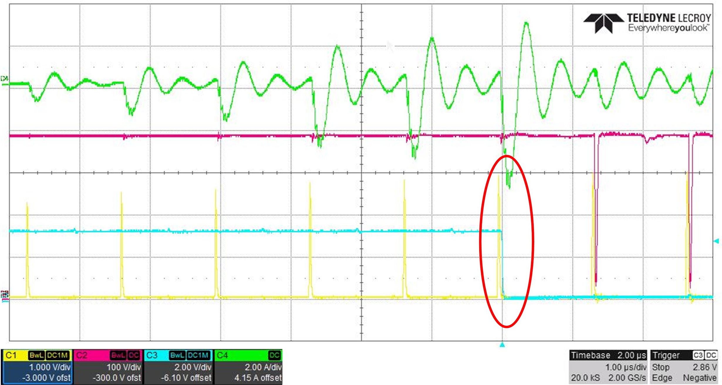
Figure 2 shows a shoot-through test on an LLC series resonant half-bridge converter with the TI LMG3410 as input switches. During the test, a high-side switch is forced on, with the low-side switch controlled by a driving signal with gradually increased duty cycles. Once the OCP trips, the LMG3410 quickly disables its driver inside to turn off the switch. This prevents the device from catastrophic failure.

Figure 2: An TI LMG3410 shoot-through test on an LLC series resonant half-bridge converter: C1 = low-side switch driving signal, CH2 = switching-node voltage, CH3 = high-side switch driving signal, CH4 = primary inductor current

We also tested LMG3410 OTP on the same LLC series resonant half-bridge board with an improper dead-time setting to force the converter into hard-switching operation. You can watch the OTP testing video.

With OCP and OTP built into this zero Qrr GaN device, you’ve cleared the most worrisome issues of totem-pole switches. Contact your local TI representative to get a LMG3410 daughtercard to evaluate how TI direct-drive GaN devices improve system reliability and efficiency.

Additional resources


I got an interview! Now what?

$
0
0
Congratulations! You’ve scored an interview with a company on your wish list, and are one step closer to getting an offer. So now what do you do? Prepare!  The process of preparing for the interview is critical. It’s like studying...(read more)

Real-time temperature sensing with dual-mode connectivity

$
0
0

Today, there are many applications that require accurate and continuous temperature sensing to protect a product or improve system performance.  Temperature sensors now have the ability to deliver accurate measurements wirelessly and in real-time thanks to advancements in connectivity technology. In many applications, the ability to monitor and control a system from a remote location is a key requirement. By combining long-range Sub-1 GHz networking with Bluetooth® low energy (2.4 GHz) connectivity opens up a world of possibilities for temperature measurement. Here we will discuss how the use of these technologies together can enhance systems where temperature measurement is critical.

Some example applications - cold chain management and home automation

Temperature sensing is used in many applications and below we will look at two examples:

  • Cold chain management
  • Home automation

Cold chain management

Cold chain management is deployed to monitor and track products that are sensitive to temperature. A typical example is fresh food being shipped from a farmer and tracked all the way to the supermarket. The temperature of pallets or individual boxes is monitored to ensure the quality of the produce. While monitoring solutions exist today, the combination of Sub-1 GHz and Bluetooth low energy in a single device plus a high quality temperature sensor enables new functionality. For example, the long-range, Sub 1 GHz network enables coverage of a large area like a storage facility and the Bluetooth connectivity enables an operator (truck driver, shop assistant) to communicate directly with the pallet/box using a smartphone to check if the product has been kept at the right temperature for the duration of its journey. These technologies also allow a smartphone to be used as an Internet gateway in places where a Sub 1 GHz network cannot be implemented – for example during the truck transport. In this case the truck driver’s smartphone could be the gateway without any intervention from the driver apart from running a smartphone app in the background.  This would allow remote systems to continue monitoring the temperature of cargo.

Home automation

Localized temperature control is important for maintaining a pleasant indoor climate. By wirelessly connecting sensors with ventilation/cooling/heating, it is also possible to optimize comfort while at the same time making sure energy consumption is kept at a minimum.  Many home automation systems use Sub-1 GHz technology today for its long range and low power consumption. In these solutions, temperature sensing is used in heating, air-condition and ventilation systems (windows/blinds). At the same time, Bluetooth connectivity allows users to access to the information via smartphones and tablets. Using a single device for both connection methods, such as the SimpleLink™ dual-band CC1350 wireless microcontroller (MCU), allows for simple, cost-effective systems to be developed. 

Building a dual-band, temperature monitoring system

TI’s SimpleLink dual-band CC1350 wireless MCU is a new wireless system-on-chip solution (SoC) that offers both the long range RF connectivity of the Sub-1 GHz frequency band, in addition to the simple connectivity of Bluetooth® low energy (2.4 GHz).  The small size of the CC1350 solution and its low power consumption make it ideal for building the systems described earlier.  In addition, its interfaces allow for adding a temperature sensor directly without additional circuitry.

Figure 1 below shows a block diagram of the CC1350 wireless MCU. For a digital sensor like the TMP103 (±2 degrees), TMP112 (±0.5 degrees) from TI, a digital interface like the I2C or the SMBus™ can be used for sensor configuration and collecting temperature data. Assuming that the I2C is used, there are two main ways of connecting the CC1350 wireless MCU to the temperature sensor:

  1. Using the I2C interface that is directly controller by the ARM® Cortex®-M3 application processor. The I2C module has a dedicated driver library function that is integrated as a part of the TI RTOS (real-time operating system). The SensorTag kit demo platform from TI includes the TMP007  contactless temperature sensors. The I2C software routine used to handle the sensor can be found here on dev.ti.com. This can be used as an example to handle other I2C temperature sensors as well.
  2. Using the sensor controller on board the CC1350 device. The sensor controller has its own configuration tool called the Sensor Controller Studio that contains sample code for the I2C interface. To access this code, download the Sensor Controller Studio and click on the I2C example on the front page.

Using the sensor controller will give the lowest current consumption. However, in most use cases, the temperature sensor is read out very infrequently (interval of ten seconds or more) – in these cases the difference with respect to average current consumption is negligible between the ARM Cortex-M3 and the sensor controller. A temperature read of every 10s can easily be designed to consume less than 1µA in total current consumption – including the stand-by (32kHz) sleep current consumption.

Connecting an analog temperature sensor to a dual-band wireless MCU

Analog temperature sensors such as the LMT70 can be read by using the 12-bit analog-to-digital converter (ADC) inside the CC1350 device. As for digital sensors, a user has a choice of using the TI RTOS that includes an ADC software driver run by the ARM Cortex-M3, or using the sensor controller. Examples of how to read out analog sensors can be found in the Sensor Controller Studio.

Figure 1: Block diagram of the SimpleLink dual-band CC1350 wireless MCU

Additional resources:

Updating those hard-to-reach industrial machines

$
0
0

Have you ever found yourself needing to update firmware on a product that has been released for field operation?  Lifetime dependability is not guaranteed after all, a software bug could be discovered or the program’s functionality could be further optimized after the initial release date.  Quick action is necessary to update the products which have already left the factory. 

But what if these units do not include an easily available JTAG or bootloader communication port?  What if the product itself is likewise inaccessible, located in a hard-to-reach location or in an environment that should not be disturbed or tampered with?  What tools do you have at your disposal to easily update such devices?

System-on-chip (SoC) solutions are always an option, and TI provides a wide range of SimpleLink™ wireless microcontrollers (MCUs) that implement low-power, low-cost solutions across a variety of communication protocols including Wi-Fi®, Bluetooth® low energy, 6LowPAN, ZigBee®, RF4CE™, proprietary 2.4 GHz and Sub-1 GHz technologies.  Any of these devices could wirelessly access the JTAG or built-in bootloader interface of a product using the MSP430™ MCU but are hindered by compatible communication peripherals — defined communication protocols— and the overhead from adding an extra MCU to the system.  There must be a more flexible solution available!

The MSP430FRBoot bootloader could be the answer you are looking for.  An extension of the MSPBoot main memory bootloader, MSP430FRBoot is a customizable programming solution that supports all MSP430 FRAM large memory model MCUs (where addresses can be greater than 16 bits) and furthermore demonstrates how over-the-air (OTA) updates can be realized.  With a minimal memory footprint of less than 4KB in size, this software solution illustrates the ability to update device memory with configurable entry sequences, application validation and shared interrupt vectors.

But what if wireless communication is lost or interrupted halfway through an update?  Direct memory access could leave the device in a hazardous unknown state, bricking the application and disabling further contact attempts.  No problem – simply use the dual-image feature, a mode that downloads and verifies the entirety of the transmitted code before it is copied to the device’s application memory.  If a complete download cycle is unsuccessful, no harm is done as the MSP430 MCU recognizes the issue and continues operation of the original firmware.

The MSP430FRBoot application report provides a software package that contains the necessary source code for implementing a main memory bootloader.  eUSCI supports both wired UART and wireless SPI (for use with a Sub-1 GHz CC110x RF transceiver) is provided, but the hardware layers are abstracted and as such can be ported to support a multitude of communication peripherals and protocols.  Host and target project examples are provided for multiple FRAM LaunchPad™ development kit variants to be used with a radio BoosterPack™ plug-in module, which can be directly connected to the LaunchPad kit headers and does not require any further hardware connections in order to run the provided demonstrations.  The software package furthermore includes all tools, including a txt to array converter and command linker generator script, necessary to jump-start a custom project.

What application can you imagine using MSP430FRBoot for over-the-air updates?  Log in and comment below to share your ideas.

Attending electronica 2016? Stop by the TI booth (hall A4, Booth 219) to see this demo in action.

Additional resources

PMBus benefits in multi-rail systems – Part 1

$
0
0

You can find hardware systems with multiple low-voltage rails that need regulation, sequencing and monitoring in cloud infrastructure equipment like base stations, networking switches, servers and storage, as well as test and measurement applications such as integrated circuit (IC) testers, oscilloscopes and network analyzers.

The Power Management Bus (PMBus) digital interface is a popular interface, which I discussed in another blog post, “A PMBus primer: common PMBus questions answered.”

TI has a complete PMBus power solution for systems using 48VDC on the front end and 12VDC or another low-voltage DC rail as the intermediate bus; see Figure 1.

Figure 1: 48V to point-of-load PMBus power system

The benefits of a complete PMBus solution in multirail systems are many: ease of use; reduced design time (as a new design can be generated in seconds by reconfiguring the on-chip nonvolatile memory [NVM]); reduction in overall component count and total solution cost; a unified and seamless design and programming method through a single graphical user interface (GUI); much simpler board characterization through PMBus margining; and improved diagnostics through voltage, current, temperature, power and fault monitoring.

Multirail PMBus sequencers/managers such as the 24-rail UCD90240 and the new 32-rail UCD90320 can sequence, margin, monitor and report faults for up to 32 rails using TI’s Fusion Digital Power™ GUI. They can also be stacked in fours for up to 128 rails, managed through the SYNC_CLK pin if needed.

Additionally, the UCD90240 and UCD90320 have true black-box logging that provides detailed information about all rails, General Purpose Input (GPI), and General Purpose Output (GPO) status on the first fault, as shown in Figure 2.

Figure 2: UCD90240/UCD90320 black-box logging

UCD90xxx PMBus sequencers/managers work with analog and PMBus point-of-load voltage regulators to provide a PMBus management and voltage-regulation solution in multirail systems, which almost always have one or more high-current application-specific integrated circuits (ASICs), processors and/or field-programmable gate arrays (FPGAs).

The loads require precise multiphase step-down conversion from the 12V intermediate bus to their respective rails. Typical load currents range from 50A to 200A, and the multiphase converter may require up to six phases to distribute power and thermals effectively and reduce the size and count of the inductor and output capacitors through phase interleaving.

One such six-phase converter is the TPS53667.

How does a multirail UCD90xxx PMBus sequencer come together with multiple PMBus voltage regulators in a design? The TI Designs PMBus Power System for Enterprise Ethernet Switches Reference Design is a good example, as shown in Figure 3.

The design employs a PMBus sequencer, a PMBus hot-swap IC (for the input current) and eight analog and PMBus voltage regulators, including a four-phase PMBus buck controller and a double-data-rate (DDR) termination (Vtt) switcher. The Fusion Digital Power GUI provides a graphical representation of the power tree and offers the capability to program the main parameters on the top half, while monitoring key parameters such as voltage, current, temperature and power on the bottom half.

Figure 3: The reference design’s PMBus board and Fusion Digital Power GUI

If you are designing multirail systems with high-current processors, ASICs and/or FPGAs and want to simplify your design and characterization, reduce development time, and increase your system’s diagnostic capability, consider TI’s PMBus power solutions.

Additional resources

How accurate is your battery fuel gauge? Part 2/2

$
0
0

Step-by-step calculation of gauging accuracy and other factors affecting accuracy

In part 1 of this series, I discussed the difference between measurement accuracy and gauging accuracy. I highlighted that gauging accuracy depends on the accuracy of input variables (voltage, current and temperature) into your chosen algorithm, as well as the algorithm’s robustness, or the ability to account for different battery use cases. I also pointed out that you can quickly evaluate the accuracy of a gauge by inspecting the state of charge to confirm that the gauge reports 0% near the terminate voltage and that the SOC doesn’t experience significant jumps.

An even more effective method is to compute gauge accuracy across the battery’s entire discharge profile. You can do this with the charge profile as well, but because users are more concerned about accuracy during battery discharge, accuracy is often evaluated using the battery discharge profile.

Here is a step-by-step method to calculate gauging accuracy: (Download this Excel sheet has actual numbers and formulas)

1. Start with a gauge log in Excel of the voltage, current, temperature and reported SOC. In part 1 of this series, I mentioned that you can extract the gauge log using bqStudio and a TI gauge EVM or any gauge and an Arbin or Maccor. In this example, I will describe the process using a gauge log from bqStudio  and a TI gauge EVM.

2. Create a new column for calculated passed charge (dQ). The log file should start from a fully charged state and end at the terminate voltage, where empty is reached (or wherever discharge stops). Use the Excel formula below to calculate each row of passed charge:

  • Calculated_dQ = rolling sum of current_reading * time_since_last_log_point.
  • Excel formula: (ElapsedTimeN+1– ElapsedTimeN)*|AvgCurrentN| /3600+ Calculated_dQN. (Since the unit of elapsed time is in seconds, convert it to hours by dividing by 3,600. Calculated_dQN-1 is the immediate previously calculated passed charge.)
  • FCC_true = integrated capacity, from fully charged state down to termination voltage.
  • Calculated_RM = FCC_true – Calculated_dQ.
  • Excel formula: $FCC_true – Calculated_dQN.

3. Calculate the battery’s true full-charge capacity, which is the sum of all the passed charge:

4. Create a new column and calculate the battery’s remaining capacity(Calculated_RM) at each point along the discharge profile:

5. Calculate the battery’s true state of charge(Calculated_SOC) in percentage at each point in a new column:

  • Calculated_SOC = Calculated_RM / FCC_true * 100.
  • Excel formula: Calculated_RM / $FCC_true * 100.

6. Calculate the state-of-charge error reported by the gauge at each point in a new column by subtracting the state of charge reported by the gauge from the calculated state of charge:

  • SOC_error = SOC_true – SOC_gauge.
  • Excel formula: Calculated_SOCN – SOC_gaugeN.

The Excel sheet shows the calculation details. In Figure 1, the different highlighted columns represent the different steps in the calculations. As you can see in column M, the SOC error magnitude clearly quantifies gauge accuracy.


Figure 1: Excel log showing an example for calculating SOC error

Figure 2 compares the calculated SOC and the SOC reported by the gauge across the battery’s entire discharge profile, while Figure 3 shows the magnitude of the SOC error graphically. In this particular example, you can see that the error in gauge accuracy across the entire discharge profile is less than 2%.


Figure 2: Visualization of calculated SOC vs. reported SOC across the battery’s voltage discharge profile


Figure 3: Visualization of SOC error across the battery’s entire voltage discharge profile

Changes in ambient temperature and discharge current rate can cause the battery capacity (FCC) to increase or decrease, which is an inherent battery characteristic. These changes result in sudden jumps in the state of charge, leading to an unpleasant user experience. In order to curb this, most Texas Instruments gas gauges have a special feature called smoothing. The smoothing algorithm’s main goal is to smooth out the jumps in remaining capacity and SOC over the course of battery charge or discharge. Note that if this functionality is enabled, the gauge’s reported remaining capacity and SOC will be mathematically modified and may not be a true representation of the battery’s state of charge. When calculating accuracy if this filtering is enabled, determine whether you want to use the smoothed (filtered) values or the true values: the gauge has the capability to report both.

Figure 4 compares the calculated actual SOC, the gauge-reported filtered SOC and the gauge-reported true SOC under multiload levels. You can see that the gauge-reported filtered SOC closely follows the gauge-reported true SOC.

Figure 5 compares a gauge-reported SOC error and a gauge-reported filtered SOC error. A more visible difference between the filtered and true gauge SOC would occur if there was a steep temperature change, which will result in a battery capacity change.


Figure 4: Comparison between the battery’s calculated true and gauge-reported SOC under multicurrent levels

Figure 5: Comparison of gauge-reported SOC errors across the battery’s voltage profile under multicurrent levels

Most gauge users need some capacity in the battery reserved when the gauge reports 0% without hitting the terminate voltage so that the host processor can perform a controlled system shutdown. In cases like this, when evaluating for accuracy, do not carry out your calculations down to the terminate voltage; rather, calculate to whatever voltage threshold corresponds to the amount of reserve capacity you need left in your battery.

Another factor affecting gas gauge accuracy over a battery’s lifetime is the gauge’s ability to track the battery’s changing impedance, which increases as the battery ages. TI’s Impedance Track™ gauging algorithm offers up to 99% accuracy over a battery’s lifetime due to its ability to track the battery’s changing resistances. Our compensated end of discharge voltage (CEDV) gauging algorithm offers up to 98% accuracy and accounts for aging mathematically, using a battery model that may become less accurate as the cell ages. Our Impedance Track-Lite algorithm is a simplified version offering up to 95% accuracy.

In summary, calculating state-of-charge error is a more robust method for evaluating gas gauge accuracy when compared to visual inspection, given that it provides the magnitude of error across the entire battery profile. Other considerations affecting gauge accuracy and its evaluation are smoothing activation, reserve capacity functionality and the gauge algorithm’s ability to track cell aging. For a comprehensive list of the various gauge offerings, visit ti.com/gauges.

Additional resources


Viewing all 4543 articles
Browse latest View live


<script src="https://jsc.adskeeper.com/r/s/rssing.com.1596347.js" async> </script>