Quantcast
Channel: TI E2E support forums
Viewing all 4543 articles
Browse latest View live

How to simplify high-voltage power-supply design

$
0
0

High voltage power supplies are ubiquitous whether you are designing an AC/DC adapter or your high voltage on-board power supply for industrial applications. You find them commonly to step down your high voltage input voltage to a lower intermediate voltage before you power your point-of-load (POL) converters. The design of these front-end power supplies pose unique challenges from the requirements that they have. This post is intended to give you a basic understanding of high-voltage power-supply design, and how design tools can make it simple to design for these applications. There are three main things that you need while designing for your AC/DC or high-voltage DC/DC application.

1. Understand your system requirements.

Most of you know where your end equipment will be used and whether you will need a universal voltage range (85V to 265V) or region-specific voltages such as U.S. (120V), Japan (100V), U.K. (230V) or China (220V). Also, are you designing for a charger-type application or an on-board power supply? Are you designing for a supply that needs tight output-voltage regulation? What type of isolation requirements do you have?

The answers to each of these questions will help you make appropriate trade-offs while you design. Designing for universal voltage ranges ensures operability across different parts of the globe at the expense of higher voltage-/current-rated components, which come at a higher price and footprint. Charger-type supplies typically require a constant-voltage/constant-current (CV/CC) characteristic. So selecting a controller that meets this requirement is essential.

If your power supply requires tight regulation of the output, you need to consider secondary-side regulated controllers that tightly regulate the voltage on the secondary, versus primary-side controller regulators where the output could vary with changes in the transformer or secondary diode parameters. Certain applications require that your transformer provide a certain class of isolation for safer, robust end equipment.

TI’s WEBENCH® High-Voltage Power Designer is an easy to use tool to design your AC/DC or HV-DC/DC applications.  You simply enter your voltage and current requirements and find solutions that work for your application. With the optimizer dial, you can optimize your design for cost, footprint and efficiency based on your system needs. To get started, visit the WEBENCH panel on ti.com. Figure 1 below shows a view of the power solutions generated by WEBENCH Power Designer.

Figure 1: WEBENCH Power Designer with High Voltage solutions

Figure 2 below shows an AC/DC flyback using primary-side regulation that provides a low-cost, low-footprint solution, as well as loose regulation of the output on the secondary. Figure 2 shows an AC/DC flyback in secondary-side regulation using optocoupler feedback, which is more expensive but provides tighter regulation on the secondary.

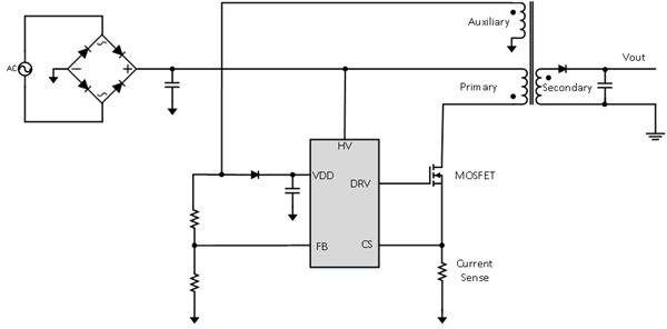
Figure 2: AC/DC Flyback with primary-side regulation


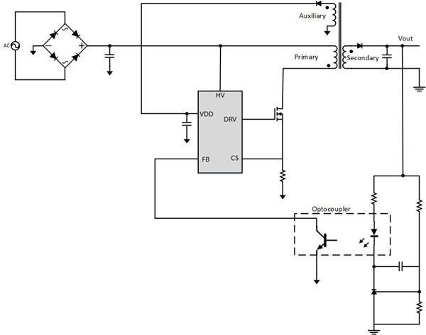
Figure 3: AC/DC Flyback with secondary-side regulation using optocoupler feedback

2. Select the right topology/control scheme.

At low power (greater than 10W and less than 100W), flyback is the most widely used topology. Forward and half-bridge topologies typically serve power levels from 100W to 500W, with full-bridge topologies serving >500W. Theoretically, you could build a flyback for high power levels too, but the voltage/current stress on the components makes this topology require higher voltage-/current-rated components, which are expensive and bulky. This paves the way for the natural adoption of other topologies at higher power levels.

You could design the controller to operate in continuous conduction mode (CCM) (the magnetizing current in the transformer does not reach zero), discontinuous conduction mode (DCM) (the magnetizing current reaches zero and stays zero till the next switching cycle), or transition mode (TM) (the magnetizing current reaches zero and the next switching cycle starts immediately). CCM is typical for higher power levels, while DCM and TM provide lower-loss solutions.

WEBENCH Power Designer saves you time and effort by creating the complete design for the topology using the necessary equations depending on the device and its operating mode. The tool also lets you evaluate efficiency and also other parameters such as output ripple, the RMS currents, losses etc. at various operating points within the design range.

3. Design your transformer.

One of the main things required in a good high-voltage power supply design is designing the transformer correctly for your applications. The transformer is generally the energy-conversion element in a high-voltage design, which also provides isolation between the primary and secondary.

By definition, transformers do not store energy, but transfer energy from the primary to the secondary. This is one of the main reasons why people refer to flyback transformers as coupled inductors, because components in the flyback topology store energy during the on-time of the switching cycle and then transfer that energy to the secondary during the off-time.

Transformers typically have a core (which is the magnetic element); the bobbin (or coil former), which is the plastic housing for the core (see Figure 4); and the wire that gets wound on the core-bobbin structure.

Figure 4: Core, coil former and assembled transformer

Assembled pre-built transformers are readily available from manufacturers with a fixed turns ratio (Ns/Np) and primary inductance (the magnetizing inductance of the transformer that causes energy to build up). Depending on the operating frequency and output power levels, the requirements for the primary inductance and the turns ratio vary widely, and a pre-assembled off-the-shelf transformer might not be available. In such cases, selecting a transformer core and bobbin and winding the transformer will be necessary. This requires an in-depth knowledge of transformer magnetics.

WEBENCH design tools now give you the ability to design the transformer by selecting the core and bobbin that meet the requirements and also provides the winding structure details as well. You can click on the transformer symbol in the schematic to view and download the transformer details and also to change the transformer core/bobbin combination. Figure 5 shows a view of the transformer design window giving you the various core/bobbin combinations for a specific design requirement. You can also compare different transformers in terms of height, losses (core/copper losses), footprint and cost. If you have a preference for a specific core type or material, use the transformer listing to pick the one that is appropriate for your needs.

The transformer construction diagram gives you instructions on how to wind the transformer. This along with the transformer construction details table gives you information on the number of layers, strands, the AWG of the wire and more. You can also download the transformer design report as shown in Figure 6 to get this information. This will simplify your effort to build the transformer whether you are prototyping it yourself or having it wound by a transformer winding company. 

Figure 5: Transformer design capability in WEBENCH


Figure 6: Transformer Design Report

Additional resources


What’s next for Industry 4.0? The best new technologies shaping the future of smart factories

$
0
0
Co-authored by Miro Adzan and Thomas Leyrer Today’s end-equipment markets demand shorter product life cycles, more individually configured products and fast adaptation to quickly changing consumer interests. On the manufacturing floor, key parameters...(read more)

Five benefits of enhanced PWM rejection for in-line motor control

$
0
0

There’s almost always more than one way to solve a problem. Sometimes the most widely used method doesn’t yield the biggest benefit.  System designers working on motor control projects use various current measurement methods to ensure the motor is running efficiently and to prevent possible damage.  There are three main methods to measure current in a motor design. In this post, I’ll review these three methods and share the top 5 advantages for in-line motor current sensing using enhanced pulse width modulation (PWM) rejection.

As Figure 1 depicts, there are essentially three different methods to measure current in three-phase motor-drive systems: low-side, DC link and in line. While Figure 1 shows the traditional three-phase PWM inverter needed to drive a DC motor with the three pairs of power MOSFETs (insulated-gate bipolar transistor IGBTs are very common as well), the figure also includes high-side current sensing which is typically used for gross fault conditions such as a short to ground.

Figure 1: Various current-sensing methods for three-phase motor-drive systems

Many designers use the first two methods (low side, DC link and various combinations thereof) because standard current-sensing solutions are readily available – typically with fast response times, higher bandwidths, fast output slew rates and low common-mode input voltages. But just because products are available that can sense phase current via low-side or DC link doesn’t mean that these solutions represent the easiest way. The idea behind measuring current in these fashions is to try to replicate the current being driven into the motor windings. This replication effort occurs in software; it can be quite involved and is never truly exact.

The in-line current sensing method seems to be the most logical because that is the current you are ultimately trying to measure, but there is a challenge with this approach. The PWM signals driving the MOSFETs or IGBTs wreak havoc on the current-sense amplifier. The common-mode signals at the sense resistor are driven from the supply voltage to ground with very fast transient switching characteristics, while the current-sense amplifier is trying to measure a small differential signal across the sense resistor itself. Figure 2 is an oscilloscope shot of the sinusoidal phase current (red waveform) generated by the PWM inverter.  In this case, the PWM frequency is 100 megahertz (MHz) sourced by the LMG5200 GaN Half-Bridge Power Stage (more details can be found in the TI Design stated at the bottom).  Note the fast switching signals are what the in-line current sense amplifier is subjected to as it measures the phase current. If I can use an analogy, this is like trying to measure the liquid in a cup as it floats along the sea during a hurricane. No wonder most designers use low-side sensing! Until now …

Figure 2: Measuring phase current amidst fast common-mode transients

Before describing the potential benefits, let me explain enhanced PWM rejection. Enhanced PWM rejection is active circuitry that forces the output voltage to settle much more quickly than traditional methods. As input common-mode signals with fast transitions are detected by the current-sense amplifier, these disturbances are minimized as they propagate through the device’s output. An alternate method to reduce these disturbances (or affectionately called by designers – “ringing”) is to use high-bandwidth amplifiers (in the MHz range) to settle the output as quickly as possible, but that may be an expensive proposition.

Figure 3 shows the output voltage signal for each of the phases represented without noise introduction. The red waveform is a representation of the signal to show that the power transistors, which are electronically commutated, replicate as close as possible a sinusoidal waveform to the motor.  The current-sense amplifier will experience an input common-mode voltage signal from the power-supply rail (VBATT = 48V, for example) to ground.

Figure 3: Expected voltage waveform due to enhanced PWM rejection

Benefit #1: Reduced blanking time

Common-mode PWM transient suppression allows for less “ringing” at the output of the current-sense amplifier. Having to wait for the voltage signal to settle is a major drawback, especially for systems that require low duty cycles (≤10%) because the time to take the current measurement is shortened (commonly known in the industry as blanking time).

Benefit #2: In-line current sensing

Coupled with a high common-mode input voltage, enhanced PWM rejection allows for the ability to monitor current in line. As discussed previously, the robustness of the current-sense amplifier is a necessity due to the harsh environment to which it’s exposed. Aside from this requirement, the amplifier must also have high AC and DC accuracy to provide system designers the precise current sensor measurements you can read more about in-line motor current sensing using the INA240 in a TI TechNote.

Benefit #3: Possible elimination of galvanic isolation

Another benefit from enhanced PWM rejection is subtle but important. With enhanced PWM rejection, designers may be able to eliminate the use of an isolated current-sensing device when galvanic isolation is not part of the system requirements. Customers often use isolated devices to decouple the noise generated as the PWM signals travel through the sense resistor. This decoupling is no longer needed with enhanced PWM rejection.

Benefit #4: Algorithm optimization

I alluded to this benefit earlier – algorithm optimization. With enhanced PWM rejection, the need to replicate or calculate the phase current is no longer an issue because the answer is already provided directly. Only minimal software is required to run the motor efficiently.

Benefit #5: Increased motor efficiency

Finally, I get to last benefit, which arguably matters most to designers – increased motor efficiency. Motor manufacturers and motor-drive system designers are always looking for ways to improve efficiency in the motor. High AC and DC accuracy, fast output response and reduced blanking time enable motor operation at the highest efficiency possible. Precise timing control of the multiphase motor reduces the blanking time as much as possible, which in turn maximizes motor efficiency.

Figure 4 shows the five benefits.

Figure 4: Five benefits of enhanced PWM rejection

The INA240 current-sense amplifier from Texas Instruments incorporates enhanced PWM rejection which brings with it a wealth of system-level benefits to your motor design. See www.ti.com/currentsensing for more information about the INA240 and other current sense amplifiers.

Additional resources

MCUs can recognize what you say

$
0
0

In our connected world we are seeing more electronic devices that understand speech. Smartphones, tablets and laptops include apps like Siri or Cortana that let help you search for answers, control the electronics around you and more. While these apps are impressive, they also take a lot of processing power and memory. So it is not a surprising misconception that microcontrollers (MCUs) are just too small to recognize speech.

It is true that the low-power and small size goals of an MCU may not allow it to understand everything someone could say but for small low-power embedded applications, all you may need is to recognize a few well-defined phrases. For example, like “heat up my coffee” or “turn the lights off.” Recently we have demonstrated this feature on our low-power MSP432™ MCU.

We have released a speech recognizer library written in C code that can enable a MSP432 MCU-based application to recognize your own personal speech phrases. It recognizes up to 11 phrases while ignoring other speech. You do have to tell the recognizer your phrases by saying them a few times but once that’s done, it’s ready to go.

The library has features that you would expect such as:

  • You can change the phrases any time you want
  • It can be instructed to respond to only a few of the phrases
  • And of course, you can delete a phrase from your repertoire if you wish

The library comes with some easy to use header files and user and API guides to get you up and running quickly. The download also includes an example demo program targeting the MSP432 MCU LaunchPad™ development kit, Audio BoosterPack™ plug-in  module, and either the Sharp or Kentec LCD BoosterPack  kit. 

The demo app uses the 14-bit analog-to-digital converter (ADC14) integrated in the MSP432 MCU to gather speech, and the LCD to display menus. The menus allow you to run recognizer features. You can choose to:

  • Say a phrase that you want the recognizer to remember. It will create a model of that speech and store it in flash memory (a task called enrollment).

  • Say an enrolled phrase again. The recognizer will use it to make a better model for improved performance (a task called update).
  • Delete a model that has been enrolled
  • Run recognition

So, what are your ideas for MCU-based apps and devices that could be voice enabled? I’d be interested in hearing. But now I think I’ll take a break to “Heat up my coffee.”

Attending electronica 2016? Stop by the TI booth (hall A4, Booth 219) to see this demo in action.

Additional resources:

Connecting sensors to the cloud at a distance

$
0
0

If you search for examples of devices in the Internet of Things (IoT), you may find mockups of connected toasters, lipstick and toy cars. You may find images of talking fridges that alert you when the milk runs out, or demos of dolls that learn a child’s favorite jokes and games. You may find visions of connected factories, farms and cities

Some of these are fun examples you may find when searching about IoT, but sprinkled in with all the fun are the “behind the scenes” devices: the temperature sensor on that toaster and fridge, the accelerometer on that toy car and doll, the pressure sensor on the lipstick. The connected farms may sport humidity sensors for crops, and factories might use accelerometers on machinery for sensing if maintenance is required. All of these sensors need to be connected to the cloud to easily access the data however, connecting them is a challenge that consumes precious time and resources.

TI’s Sub-1 GHz Sensor to Cloud with Industrial IoT reference design (TIDEP0084) takes this challenge and streamlines the connectivity process. An engineer looking to connect a device can start working from a proven design instead of having to be the total expert on wireless connectivity. They can easily leverage this reference design as a base or foundation for integrating Sub-1 GHz technology into their current and future products.

The design demonstrates how to connect sensors to the cloud over a long range Sub-1 GHz wireless network, suitable for industrial and consumer applications. It is powered by a TI Sitara™ AM335x processor and SimpleLink™ Sub-1 GHz CC1310 and dual-band CC1350 wireless microcontrollers (MCUs). The reference design pre-integrates the TI 15.4-Stack software for Sub-1 GHz star network connectivity and the Linux® TI Processor SDK. TI Design Network partner stackArmor supports the cloud application services for cloud connectivity and visualization of the sensor node data. Basically, the TI Design reference design integrates both hardware and software components for a seamless design experience. 

Figure 1: Diagram of the Sub-1 GHz Sensor to Cloud with Industrial IoT reference design

Building a scalable network doesn’t need to be a cumbersome task. By leveraging the Sub-1 GHZ Sensor to Cloud design, you can easily connect one, two, three, or up to 50 devices in a modular, plug-and-play kind of way. The SensorTag kit in the design comes with infrared, humidity, light, pressure, and more sensors all operating on a single coin cell battery. Every single bit of data seamlessly connects to cloud application providers like Amazon Web Services, Microsoft Azure or any standard cloud interface with the support of stackArmor.

Even with all of this capability, the end goal is to solve a problem. An example used previously was an accelerometer in a factory. A factory using mechanical devices like cranes and lifts will need to service them regularly for performance and safety. How does a technician know it needs to be serviced? Instead of having to react to a breakdown or guess, an accelerometer on the device could detect irregular movements. Instead of having to install expensive wiring to the device, the accelerometer could be connected wirelessly and at a long range. Instead of having to manually download every bit of data, the sensor could stream directly to the cloud and alert the technician instantly. The Sub-1 GHz Sensor to Cloud reference design handles every step in this process seamlessly.

Happy designing! To start, visit www.ti.com/sensor2cloud and then order the kits you need:

Enjoyed this topic? You might enjoy reading these other blog posts:

Rise of the industrial robots. Overcoming the challenges of safe robot-human-interaction in factory automation

$
0
0
“I’ll be back.” That’s probably the most famous sentence ever uttered by a robot. At the same time, it’s probably also not the best promotion for robotics as the Terminator does everything but act like a friendly human...(read more)

Automotive Imaging is making your car safer

$
0
0

In October of 2002, Cameron Gulbransen was killed by his father,  Greg Gulbransen, who was slowly backing his SUV out their driveway and did not see his son run behind the car due to the large blind spot behind his SUV.  Little Cameron ran into that blind spot and was accidentally run over.

This was a turning point in the effort to install electronic cameras in automobiles to help improve safety.

Greg promised himself that what happened to his little boy would never happen again to anyone else. He joined KidsAndCars.org, a child safety advocacy group, and started a campaign to eliminate the blind spot behind cars by installing an electronic backup camera. After a 12-year campaign, he finally succeeded.  The U.S. Dept. of Transportation’s (DOT) National Highway Traffic Safety Administration (NHTSA) announced on March 31, 2014 the requirement for rear visibility technology cameras in all new vehicles under 10,000 pounds by May 2018.  “Rear visibility requirements will save lives, and will save many families from the heartache suffered after these tragic incidents occur,” said NHTSA Acting Administrator David Friedman.

The DOT estimates that 210 deaths and 15,000 injuries are caused every year by back-over accidents in the U.S., the majority of which involve children and senior citizens.  KidsAndCars.org estimates that 1,126 children lost their lives due to back-over accidents between 1991 and 2012.  A majority of these deaths could have been prevented by backup cameras.

Many manufacturers did not wait for the mandate to be in place, and started installing backup cameras as an option.  By 2012, nearly half of all automobiles sold in the U.S. were already equipped with this feature, and many aftermarket manufacturers started making kits to retrofit older cars.  This was the start of the “imaging revolution” in cars. 

Now camera based active safety systems are rapidly multiplying in cars.  In addition to backup cameras, your typical 2017 model year car may also have the following:

  • Surround view system using four cameras
  • ADAS front camera system with up to three cameras
  • Rear mirror assist camera
  • Security camera
  • Driver monitoring camera
  • Side view cameras

Many new models from 2017 onwards will have more than 12 cameras to help enhance safety.


 Figure 1.  Automotive cameras


                           Figure 2.  Typical Electronic Digital Camera

A typical electronic digital camera consists of a lens to capture light, and an image sensor that converts the light into electrical signals on an array of photo-sensors called pixels.  These pixel signals are then fed into an image signal processor (ISP) for processing into the desired image, and then sent out to a display for viewing, compressed for storage or sent out for further computer vision analysis.

Cameras on automobiles can be divided into two categories – those for visual display and those for machine vision. Cameras for visual display present an image to the driver on a display screen in the cockpit. Examples of these applications are:

  • Backup camera
  • Surround view system using four cameras
  • Rear mirror assist camera
  • Security camera
  • Side view cameras – either to augment mirrors or even completely replace them
  • Night vision cameras

Cameras for vision or analytics applications generate an image for use by a vision processor which runs analytics on pixel data to perform Advance Driver Assist Systems (ADAS) functions.  The analytics functions run on a custom TI heterogeneous architecture called Vision Acceleration Pac consisting of custom built embedded vision engines (EVEs), working in tandem with industry leading TI C6000™ DSP and ARM® cores.  EVE is a specialized fully programmable TI vector processor designed to efficiently process low-level and mid-level computer vision algorithms at very high speed.  It complements the TI C6000 DSP which excels at processing high level vision algorithms. Examples of analytics applications are:

  • Adaptive cruise control (ACC)
  • Adaptive high beam
  • Blind spot monitor
  • Collision avoidance system
  • Forward collision warning
  • Intelligent speed adaptation or intelligent speed advice (ISA)
  • Lane departure warning system
  • Driver monitoring system – for drowsiness and distraction detection

Requirements for image processing for visual use-cases are significantly different than those for vision/analytics use cases. Visual use-cases focus on providing the best perceptual image quality to a human viewer, emphasizing visually pleasing color and tone, lower perceptible level of noise, increased dynamic range and edge enhancement to sharpen the image. These requirements map directly to the perception of the human visual system.

Analytics use-cases on the other hand, do not care about perceptual image quality as they focus on a class of image processing algorithms which aid computer vision. Consequently, algorithms which increase perceptual visual quality, for example color correction and white balance correction, are not needed when processing for analytics.

ADAS applications rely on cameras to provide a digital video stream for computer vision algorithms to help with safety and driver comfort. The video stream must be of high quality, free of defects, real-time and have low latency.  It must be able to handle typical automotive challenges of wide field of view and high dynamic range. Finally, the camera system should be able to operate within a low power and thermal budget, and maintain signal integrity over a wide variety of temperature and weather conditions. 

                                  Figure 3.  Typical vision analytics processing flow

Texas Instruments (TI) has a long history of in electronic imaging and digital signal processing.  In 1972, the very first patent in the world for an electronic camera system was issued to TI.   Since then TI has leveraged its many years of image signal processing experience into the design of ISPs for many applications such as digital still cameras, mobile phones, surveillance cameras, traffic cameras, and most recently now automotive visual and vision cameras.

The TDA3x System-on-Chip (SoC) has a 6th generation ISP that performs advanced image processing on image signals coming from up to six cameras.  It can either output those images to a display or feed them into its programmable DSP/EVE compute engines to execute machine vision algorithms.  The heterogeneous image processing architecture on the TDA3x is flexible and powerful enough to solve any Automotive Imaging Problem, including new unexpected ones.  This is very important, as automotive imaging is still a new and developing field with many new applications and requirements being presented.

           Figure 4.  TI TDA3x SoC Block Diagram

The automotive imaging environment is very challenging.  Cameras have to work reliably under temperature extremes and in all weather conditions, including high dynamic range situations with extreme brightness and darkness.  New technologies such as LED lighting systems bring on new challenges such as LED flicker.  In addition, many of these functions can be safety critical. If the camera does not perform correctly, safety may be compromised.  It’s a much more challenging situation than that of your typical mobile phone camera.

To help further enhance safety, reliability and robustness under a wide variety of conditions, more than one type of sensor is often needed to view the same scene.  As an example, visible light imaging can be combined with radar imaging to work together to help improve safety.  Radar and imaging sensors are very complementary.  Imaging brings the advantages of high resolution, ability to identify and classify objects, as well as providing vital intelligence.  Radar, on the other hand, can see in darkness, through fog rain or snow, and can measure distance and motion very quickly and effectively.  The visual and radar images can be processed and fused together on the TI TDA3x or TDA2x processors to provide a solution that is much more robust.

Automotive imaging is a new and rapidly developing field that is helping to make cars safer, and ultimately in the not too distant future, enabling them to drive themselves.  Automotive Imaging applications have to be robust enough to work in a wide range of challenging real world conditions. TI has developed a heterogeneous signal processing architecture on the TDA3x that is flexible and powerful enough to address any automotive imaging challenge, including new unexpected ones.

The TDA3x is currently being designed into the full range of automotive imaging applications.


   Figure 5.  Typical difficult automotive scenes handled by the TDA3x

Dear factory manager: With predictive maintenance, you can prevent problems before they happen

$
0
0

Predictive maintenance graphic

Having your home heating, ventilation and air conditioning systems inspected occasionally is a good example of preventive maintenance – and important to keeping them running properly. But what if you could predict that the heater will go out in exactly two months – during the dead of winter?

With the right information, you could plan accordingly, replace the unit, and avert the need for emergency repairs and other inconveniences that come along with them.

“Often we only find out that something is faulty when it stops working,” said Dave Smith, MSP430™ microcontroller (MCU) product marketing engineer. “In some situations, we use preventive maintenance on a fixed schedule to try to avoid these unforeseen failures.

“Predictive maintenance goes a step further by adding a level of intelligence into the equation.”

Factory settingThat’s exactly what we are doing at TI: adding a level of performance to our MCUs to help enable applications like predictive maintenance. (Read a white paper about predictive maintenance.)

Imagine: If this type of predictive maintenance could help you avoid a mini-emergency at home, what could it do for a factory full of electronics and equipment?

New TI devices

We have several new devices that present intriguing possibilities for factories. For example, the SimpleLink™ dual-band CC1350 wireless MCU and the low-power, high-performance MSP430FR5994 FRAM (ferroelectric random access memory) MCUare designed for end applications such as ultrasonic metering, portable health devices, and building and factory automation equipment.

The FRAM MCU has up to 40 times the performance of similar MCUs on the market and could be used to analyze vibrations for predictive maintenance in factories, Dave said.

Also, we just announced our latest high-performance, 80-volt current sense amplifier, the INA240, which can detect shifts in operating current levels in factory equipment. This can help diagnose the overall health of the equipment and indicate potential failures before they happen.

“Its ability to work in a tough switching environment and provide the most accurate measurement on the market is amazing,” said Jason Cole, a product line manager. “Designers who have to deal with these types of applications truly understand the value of accurate, low-drift precision measurements.”

We unveiled the INA240 today at Electronica.

So what exactly is predictive maintenance? Essentially, it’s when connected machines can tell you they're going to fail before they fail. It can help companies save millions of dollars by predicting failures and reducing unplanned down time. This helps keep end equipment customers happy.

Replacing traditional preventive maintenance with innovative predictive maintenance will not only reduce factory down time, but it will also improve safety and reliability in factories and save money on parts and labor.

“Rather than experiencing a failure, an engineer can be sent out to replace the faulty component sooner,” Dave said.

He cited an industrial motor or pump as an example.

“Even the smoothest motors give off small vibrations. By measuring and looking for changes in these vibrations, we can determine whether the motor is running well or if some unseen wear is occurring,” he said.

Predictive maintenance is here today and can be easily integrated with current factory communication systems. It can be designed into new production processes or retrofitted into existing processes.

Introducing the low-energy accelerator (LEA) 

Our new 16-bit MSP430 MCU is the first device to include a low-energy accelerator (LEA) – an accelerator that is highly optimized for ultra-low power, signal processing applications. This new peripheral extends the reach of the MSP430 MCU’s processing ability within certain applications.

The LEA module’s signal processing capabilities will also help designers develop more compact and simpler embedded systems that are needed to analyze vibrations in factory equipment.

“Today these systems are expensive, complex and power hungry. Our device can help reduce the system cost and complexity to enable more predictive maintenance systems to be implemented,” Dave said.

Today’s systems are typically limited to expensive industrial installations. In the future, we will have predictive maintenance in our home HVAC systems so we can reduce system failures.

Our device could also have a positive environmental impact: By reducing power, we are essentially extending battery life, which in turn reduces the number of batteries that are being disposed of. This is difficult to quantify, however, as it depends on the application and how much the LEA module is used, Dave said.

“For many battery-powered applications where there is a limited amount of energy available, this device with the LEA module can provide a much more energy-efficient solution,” he said.

Learn more about SimpleLink CC1350.


Extend the input-voltage range of boost controllers

$
0
0

I was recently reading an amusing article posted on The Telegraph titled “50 technological advances your children will laugh at.” It is incredible to see how quickly technology is changing, and how must-have gadgets from one decade become the big, clunky gadgets that kids start laughing at the next decade.

With the increasing number of electronics being powered off of lithium-ion (Li-ion) batteries, it is important to design an efficient and robust power supply. Just take a look around you: I am sure you have at least two or three electronic devices that are being powered off of a battery source. I recently got a new laptop computer and I am impressed with the sleek, compact design that still provides excellent battery life. However, you have to keep in mind that Li-ion batteries will constantly charge and discharge, which will affect the operation of other integrated circuits within the system.

Wide input voltage range DC/DC controllers usually have built-in undervoltage lockout (UVLO) circuits to prevent the converters from misoperating when the input voltage is below the UVLO threshold. In the event of a load transient or a supercapacitor discharging, the input voltage may drop below the UVLO threshold, causing an undesirable shutdown of the system. Furthermore, these controllers generally cannot be used in applications where the input voltage is always lower than the UVLO threshold. You can consider a split-rail approach to extend the boost converter’s input voltage range, however, enabling the use of these controllers in applications where the input voltage is lower than the UVLO threshold.

Texas Instruments’ TPS43060 and TPS43061 low quiescent current synchronous boost DC/DC controllers with wide input voltage ranges are used commonly across 5V, 12V and 24VDC bus power systems. Synchronous rectification and a compact 3mm-by-3mm 16-pin solution enable high efficiency and high power density for high-current applications. The TPS43061 is an example of a boost controller that can support a split-rail configuration. As shown in Figure 1, the input supply to the boost converter can split into two rails: the power-stage input rail and the controller’s bias input rail. The power-stage rail is the input to the boost converter for power conversion. The bias input rail is used to power the controller itself, which can be an additional auxiliary supply or derived from the output. With the split-rail configuration, the TPS43061 can support an input as low as 1.9V.

Figure 1: Split-rail configuration

In some applications with only one input supply, the input supply voltage may be greater than the UVLO turn-on threshold at startup but may fall below the range afterwards, causing an undesirable shutdown. One example is a power system using a photovoltaic panel combined with a supercapacitor as an input supply; the input voltage may drop below the UVLO threshold due to the discharging capacitor. For this type of application, if the output voltage is within the bias input specification range (or, in other words, if VOUT is greater than the UVLO turn-on threshold), then VOUT can be fed back as the bias supply through a diode, as shown in Figure 2.

Figure 2: VIN biased from VOUT of TPS43061

With Li-ion batteries used across several applications such as smartphones, tablets and laptop computers, the voltage of a single-cell Li-ion battery can range from 2.7V to 4.2V due to discharge and charge. For these applications, you need a separate bias supply other than the battery input. As shown in Figure 3, a 4.5V or higher source connected to the bias rail can power on the controller. Since the bias supply needs to supply low voltage, you can connect another supply rail within the system above the UVLO turn-on threshold to the bias rail. Another approach is to add a charge pump that can produce the bias voltage.

Figure 3: VIN biased from an additional supply

A split-rail approach separates the power rail from the bias supply rail to eliminate the constraint on the minimum operating voltage of the power rail. By extending the input voltage range of the boost controller, you’ll have more time to design the next must-have gadget. Consider TI’s TPS43060 and TPS43061 low quiescent current synchronous boost DC/DC controllers for your next split-rail design.

How to improve IoT designs with a nanopower EMI-tolerant op amp

$
0
0

Designers of Internet of Things (IoT) applications have two primary concerns: managing power to maximize battery life and ensuring reliable operation against all sorts of electromagnetic interference (EMI). The IoT revolution will lead to the deployment of billions of battery- and line-powered connected devices, many of which will be wireless, all vying for the same spectrum of frequencies. This will create an increasingly noisy environment, with electromagnetic waves radiating from multiple sources. Interference from electromagnetic signals has been a problem of the shared unlicensed spectrum since the introduction of wireless devices, but the magnitude of the problem increases when the number of devices in operation multiplies. End equipment such as smoke detectors, toxic gas sensors and PIR sensors which have wireless capability need to be tested for additional radiation EMI tests because of their interactions with each other as shown in Figure 1.

Figure 1: Passive infrared (PIR) sensor and carbon monoxide detector with electromagnetic waves

The race to create wireless sensing nodes has brought in a degree of complexity to EMI testing. System designers need to carefully select components to avoid expensive redesigns that could delay time to market in the final stages of product development. In addition to working under noisy conditions, battery powered connected devices will also need to operate reliably for years without the need to change batteries. The battery life of IoT devices varies greatly, from hours to years, depending on the application and its operating environment. Designers of these IoT devices will have to choose components that consume very low current to extend operating life and offer EMI immunity.

TI’s LPV811 family of nanopower amplifiers consume quiescent current as low as 320nA to maximize battery life and are internally protected from EMI. These devices do not, however, include the full input EMI filter seen on many recently released operational amplifiers. We at TI did this intentionally, as adding an input EMI filter greatly increases the input capacitance, which can cause peaking in sub-microampere circuitry with large feedback resistor values and source impedances. Instead, we employed internal (proprietary) precautions in the layout and internal design of the LPV801, LPV802, LPV811 and LPV812 to make it as EMI-hardened as possible.

To verify the effectiveness of our built-in EMI mitigation technique, we compared the LPV802 against two popular competitive devices that do not have internal EMI protection. Under all conditions, the circuit using the LPV802 demonstrated better EMI immunity than circuits using competitive devices. We tested all three devices for EMI tolerance under IEC 61000-4-3 (Electromagnetic Compatibility (EMC) -radiated test conditions. We subjected the devices under test (DUT) to a calibrated radio frequency (RF) field over an 80MHz to 6GHz frequency range while monitoring the DUT for malfunctions in accordance with the IEC 61000-4-3 EMC-radiated specification. To compare the three devices, we exposed all three devices to the same EMC radiation at the same time in identical circuits and monitored their output for deviations. In addition, to gauge the effectiveness of a common EMI filtering technique, we tested two sets of boards. One set of boards had added external input EMI capacitors, and one set did not have EMI capacitors.

Figure 2 shows the test board built on a standard 62mil, two-layer FR4 board, with ground planes on both sides to test EMI performance. A four-pin connector enabled quick board changes. Socketing the sensor pins enabled easy removal of the sensor.

Figure 2: Test board with sensor

Figure 3 shows the test setup in the chamber. There were four boards for testing EMI performance. Three of the boards had identical circuitry, with different operational amplifiers mounted on them. One extra board was built in a ground-reference configuration but was not used in the test. We connected each of the four boards to a central battery box (2 x AA cells) through 1m of four conductor-shielded cables with EMI chokes on both ends. We connected the battery box to the control room via 15m of UTP CAT-5 cable, with appropriate EMI chokes, to deliver the output voltages to the logging system. The two white boxes with the cones are the field sensors for monitoring the field during the test.

Figure 3: Test setup for IEC61000-4-3 EMC-radiated test

Figure 4 shows the results of one of the IEC 61000-4-3-prescribed tests. At 30V/m radiation levels, both competitive devices start failing at 140MHz, while the LPV802 held down to 100MHz. In general, the EMI performance of the circuit using the LPV802 was better than the circuits using competitive devices for all of the prescribed tests at different radiation levels, particularly in the 100-200MHz range. All of the devices were mostly unaffected by the upper (>400MHz) frequencies. For details regarding test conditions and results, refer to the application note, “Comparing EMI Performance of LPV802 with Other Devices in a Gas Sensor Application.”

Figure 4: Results of 30V/m test with capacitor

Adding external EMI input capacitors also helped overall performance, and I recommend adding them as part of the normal design process. EMI protection does not completely eliminate the effects of EMI, but it does help reduce the effects.

Adding external filtering further reduces the effects, and I recommend external filtering even when using EMI-protected devices.

Using components like the LPV801, LPV802, LPV811 and LPV812 that consume nano-amperes of quiescent current and are EMI hardened helps designers to build systems that have longer battery life and that are compliant with worldwide EMI regulations. This helps reduce maintenance costs, improve time to market and eliminates the need to do expensive re-designs due to failure in EMI in the final stages of product development.

Additional resources

High performance and low power…The original dynamic duo

$
0
0

Peanut butter and jelly.  Pizza and Monday night football.  Milk and cookies.  What do all these things have in common?  They make a perfect pair.  Likewise TI’s MSP432™ microcontroller pairs perfectly with TI’s new pre-certified SimpleLink™ Bluetooth® low energy module.  This textbook combination makes it seamless to add Bluetooth low energy connectivity to any application. 

From healthcare to factory automation, the need for wireless connectivity stems far beyond personal gadgets and activity trackers.  Let’s take a look at one example where TI’s twosome, the MSP432 MCU + CC2650MODA module, amplifies the way we’ve traditionally monitored our homes for carbon monoxide or radon gas leaks (Figure 1). 

Figure 1. Carbon monoxide detector

Imagine creating a product that captures higher precision air quality measurements and can easily transmit data to a smartphone that has a rich graphical display to monitor results.  This takes home gas detectors to the next level of innovation.  Users can receive an alert on their phone before the batteries in the carbon monoxide detector need to be replaced.  Detection systems will no longer need reset buttons or display screens because they can be controlled by a tablet.  This can reduce the size and cost of many carbon monoxide or radon gas detectors.  With TI’s MSP432 MCU and Bluetooth low energy module, gas monitoring applications can be designed to exceed homeowner’s expectations without increasing design effort.

Both of these devices perform exceptionally on their own: The MSP432 MCU is ultra-low power with an integrated 14-bit SAR analog-to-digital converter (ADC) capable of 1Msps sampling rate and floating-point digital signal processing (DSP) instruction set to process the most precise measurements.  The Bluetooth low energy CC2650MODA module is pre-certified with completely integrated hardware and software to reduce development time and simplify procurement.

Now combine these two devices together and it’s a great marriage between high performance and low power.  With TI’s BLE-Stack simple network processor software, the MSP432 MCU handles all the user application code and the CC2650MODA module runs the Bluetooth low energy related processing.  This minimizes the RF design effort as users only have to configure TI’s simple network processor API not the whole protocol stack.  There is increasing platform continuity as both devices are low-power ARM® Cortex®-M based and are easy to use with TI’s highly flexible software development kits.     

The evaluation process is even simpler with TI’s bundle pack featuring the MSP432 MCU LaunchPad™ development kit and the CC2650MODA module BoosterPack™ plug-in module and there is an example code available on TI Resource Explorer to build your first Bluetooth low energy project (Figure 2).


Figure 2. MSP432 LaunchPad development kit with the CC2650MODA module BoosterPack kit

Ready to see this dynamic duo in action?  Stop by the TI booth (hall A4, Booth 219) at electronica 2016 to see our demo showcasing the precision and scalability of the MSP432 MCU and the CC2650MODA module.

Figure 3.  Visit TI at electronica 2016

Learn more:

Power designs require powerful tools

$
0
0

Your boss just asked you to create a voltage regulator design to power the latest board revision. Do you have all the tools you need to create your design?

  • Brain, check.
  • Books, check.
  • Coffee, check.
  • Tools, hmmm ... maybe …

You probably know the steps you have to take, and of course, you have Google to search for anything not covered in your books or that you might have forgotten about power design (or face it, maybe never knew). You probably have a tool to create your circuit schematic, and you either have a calculator or your computer to calculate the equations. You might even have a SPICE simulator to dive deeper into transient behaviors.

OK, now you’re depressed … am I right? It looks like mountains of work with hurdles to jump, and a headache from the review of multiple datasheets, intense simulation model search and CAD tool updates to ensure it is all compatible, but it’s not.

On top of tool-related struggles, there are the typical power design challenges. You have to carefully consider selecting the right inductors, FETs, diodes and capacitors that will maintain the essential stability requirements and still achieve the necessary efficiency, all while meeting cost and size and heat constraints. You must make trade-offs. But how do you know that you are making good choices and getting the job done quickly without turning it into a research project? Your boss is waiting ...

Well, it doesn’t have to be a struggle. Powerful tools are at your fingertips on TI.com. WEBENCH® Power Designer can do the calculations, select components, make the trade-offs, create the schematic and run simulations in a few minutes and you won’t break a sweat. This tool takes you from a few specifications to a complete design, including a schematic and board layout with the full library included.

Figure 1: WEBENCH® Power Designer

Never heard of it? Worried it might be too difficult? You can learn about all the steps in detail by watching the “Learn WEBENCH Power Designer” video series.

Additional resources

(Em)brace the challenge: The Elbow Orthosis

$
0
0
For Texas A&M students Nathan Glaser, Joe Loredo, Rafael Salas and David Cuevas, their project began with a simple problem statement from their mentor: Some people are unable to lift a glass of water to their lips, so how can we help? This was th...(read more)

How to use the LDC calculations tool

$
0
0

While developing inductance-to-digital converters (LDCs) at TI, we often use a variety of spreadsheets to determine the appropriate settings or capabilities. I decided to combine all of the various tools into a single spreadsheet for convenience, and we’re releasing this spreadsheet to the web to help in your LDC system design.

The spreadsheet runs on Microsoft Excel, and you can download it here. The calculator tool doesn’t use any macros or special add-ons, so it is an easy download. While we do our best to make this tool as accurate as possible, we don’t give any warranty on the results.

The starting point for the spreadsheet tool is the Contents tab, as shown in Figure 1. This tab has a list of all the available calculation tools (see Table 1), each housed on a separate tab. Simply click the blue links to go to the appropriate calculator.

Figure 1: The Contents tab of the Excel spreadsheet

To use this tool, enter your parameters in the yellow fields; the results are in the orange fields. Don’t change the formulas in the orange tabs, or else you’ll have errors or incorrect calculations.

Calculator tab

Description

Racetrack Inductor Designer

Designs a circular- or racetrack-shaped sensor.

Sample Rate Calculator

Calculates the sample rates for various LDC devices.

Inductance and Frequency from Output Code

Calculates sensor inductance and resonant frequency based on the device output code. Can also calculate RP from the output code for the LDC1101, LDC1000, LDC1041 and LDC1051.

Skin Depth Calculation

Skin depth is important for understanding performance based on target thickness and material.

LDC161x/LDC131x Current Consumption Estimator

Estimates the current consumption for the LDC131x and LDC161x by putting the LDC into sleep mode or shutdown mode. The application note, “Power Reduction Techniques for the Multichannel LDCs in Inductive Sensing Applications,” covers this topic in detail.

LDC131x/LDC161x Sensor Configuration

Calculates appropriate settings for the LDC131x and LDC161x IDRIVE. The application note, “Configuring Inductive-to-Digital Converters for Parallel Resistance (RP) Variation in L-C Tank Sensors” has more information on this topic.

Remote Coil Maximum Distance Calculator

LDC devices can operate when the sensor is located some distance from the LDC. This tool calculates the maximum distance for a given sensor.

LDC0851 Calculator Tool

Calculates the LDC0851 functionality for a given sensor, including sample rate, current consumption and estimated switching distance.

LDC1101 Rp Configuration

Calculates the RP_MIN, RP_MAX, T1, C1, T2 and C2 for the LDC1101.

Spring Sensor Calculator Tool

While mechanical engineers think that a wound-wire coil is a spring, electrical engineers know that it is really an inductor. This tool can estimate performance when using a spring as the LDC sensor.

Table 1: Spreadsheet calculator tabs

All tabs contain a link that says Return to Main Page at the top of the tab, which will take you back to the Contents tab. See Figure 2.

Figure 2: Return link

The Quick Sensor L/C/f Calculator is shown in Figure 3. It is a simple but very useful tool located right on the Contents tab that calculates the inductance, capacitance or oscillation frequency of an LDC sensor. (Note that this calculation doesn’t work for the LDC0851, which I’ll discuss in a future blog post.)

Figure 3: Quick Sensor L/C/f Calculator on the Contents tab

First, select which parameter you wish to calculate – fsensor, L or C. Then enter the two values into the yellow fields. One nice thing about this calculator is that you can copy the 3-by-3 group of cells and paste the cells into another spreadsheet, and the copy will work independently of the original.

Right below is the Rp/Rs/Q Calculator (refer to Figure 4), which is helpful for transforming between RS and RP. It works similarly to the L/C/f calculator.

Figure 4: Rp/Rs/Q Calculator

In my next post, I will cover how to use the Racetrack Calculator tool to design a sensor.

Do you have any questions about or ideas for the LDC Calculator tool? Do you want to know more about a specific aspect of this spreadsheet? If so, log in and leave a comment below.

Additional resources

Integrated smart sensor health monitoring for ADAS and autonomous driving

$
0
0

Monitoring the status of a growing network of automotive camera, radar and other high-speed sensor modules is becoming increasingly complex. Although smart sensors with a local processor can supervise their own health status, raw data sensors often lack a local microcontroller to perform this task, leaving the central electronic control unit (ECU ) processor to monitor every sensor individually.

Raw data sensors need not be “dumb,” however. Integrating smart health-monitoring features into the serializer and deserializer (SerDes) link chipset relieves the central processor from constantly polling sensors for their operational status. In this post, I’ll take a look at one such implementation.

Multisensor advanced driver assistance systems (ADAS)

Next-generation vehicles may have a dozen or more remote raw data sensors (Figure 1). Supervising the health status of every sensor increases software overhead in the central ECU processor. The ECU must monitor factors such as sensor status, module voltage, module temperature, link operation (in both directions) and other indicators across multiple sensors, serializers, deserializers and other chips to generate a complete picture of sensor health. You could add a small microcontroller to each remote-sensor module for health monitoring and housekeeping, but this increases module size and cost – and the central ECU must still examine each sensor and link individually.

Integrating health-monitoring functions into the SerDes chipset enables collective monitoring of multiple sensor modules as well as their links, so that the central ECU receives only a single, consolidated interrupt warning.

Figure 1: Example deployment of automobile camera and radar sensors

Link status and protection

The first layer in autonomous sensor monitoring is the link integrity itself. The link must provide a robust control channel as well as link data-protection and diagnostic features. The link monitors cable faults (open, short to ground, short to Vbatt) as well as bit errors, and reports alerts back to the ECU. Both the forward channel and back channel are supervised by the SerDes chipset for faults. In addition, the DS90UB953-Q1 serializer performs a parity check on data input of the serializer, allowing the system to determine if potential errors originate from the sensor or from the link. Finally, the deserializer’s adaptive equalizer provides a cable health-quality measurement, enabling the system to warn of cable deterioration.

Sensor module health diagnostics

As sensors proliferate and system functional safety becomes more important, it is useful for individual sensor modules to provide some level of health monitoring. The DS90UB953-Q1 serializer, for example, incorporates a number of features to support this goal (Figure 2). Internally, the serializer supervises its own status, such as lock, valid clock and temperature. The serializer can also monitor external health factors such as power-supply voltages and incoming sensor data errors. A configurable alarm bit sent back continually to the deserializer warns the ECU if any monitored value is out of range. The serializer also reports if there are errors in the control channel communication to the sensor module. If an I2C write error arises, the serializer does not propagate erroneous I2C commands, thus helping to prevent sensor module misconfiguration. The deserializer delivers a warning to the central ECU so that the system can take further action such as control data retransmission.

Figure 2: Example of integrated sensor module health diagnostics

Aggregated health status

A multi-input deserializer hub such as the DS90UB960-Q1 aggregates the status of as many as four sensors to a single programmable open-drain interrupt pin (Figure 3). An alarm sent by any one of the multiple sensor serializers or links can trigger the interrupt. The local processor then reads the status registers to ascertain the nature and location of the warning. You can configure the deserializer interrupt pin to activate based on a number of programmable variables. Since the pin uses an open-drain structure, you can connect multiple interrupts together (wire OR’d) to combine interrupts from multiple chips, saving processor I/O pins.

Figure 3: A deserializer hub aggregates alarms from multiple sensor links

Smart sensor health

An increasing number of high-speed sensors are being used in automobiles, leading the way to autonomous driving. Today’s raw data sensors can incorporate health-monitoring features to remotely and autonomously monitor for faults, saving processor resources and providing an extra layer of system protection. These “health-smart” modules make it easier to deploy the larger numbers of high-speed sensors that future vehicles will require. To learn more, check out TI’s entire FPD-Link III SerDes portfolio for ADAS applications.

Additional resources


What's brewing in beer production? Industry 4.0

$
0
0

Photo credit: Technische Universität München (TUM)Beer is as much a staple of German culture as hamburgers are to America. So it’s not surprising that the Research Brewery of the Munich Technical University – situated just a short drive from our European headquarters in Freising, Germany – is using technology to take beer brewing to a whole new level.

Competition in the beer industry is fierce. The landscape is constantly shifting, thanks to the broadening tastes accompanying the rise of craft beer and the constant arrival of new varieties of hops, malt and yeast.

This means that for beer makers large and small, efficiency in the brewing process and quality of product are of utmost importance.

It’s with this background that Industry 4.0 is automating and optimizing the age old craft of producing quality beer. And TI technology is playing a role in bringing these capabilities to breweries around the world.

The art of brewing

Typically, breweries contain numerous tanks holding beer in its various stages of production. These tanks must be monitored and controlled: regulating the rise and fall of temperature, pressure and degree of fermentation is crucial to ensuring the manufacturing process is as efficient as possible – and that a high-quality beverage is produced.

Johannes Tippman (Photo credit: Technische Universität München)Although basic automation first came to beer production in the 1970s, the emergence of the IoT – sensors, data processing and the cloud – means the level of sophistication is now enabling brewers to improve their processes and products like never before.

At the Research Brewery of the Munich Technical University in Freising, brewers are applying technology innovation as they develop methods to create better beer.

One of the main challenges is consistently producing a high-quality beer.

“Everybody can brew a decent beer after 10 attempts,” explains Johannes Tippmann, master brewer at the university brewery. “The difficult part is to produce the same great beer 10 times in a row.”

Industry 4.0 in action


In an effort to achieve this consistency, the Research Brewery is making use of technology, including automation, analytics and management systems, to optimize different parts of the brewing process.

As part of this work, the Research Brewery uses our ADS1257 analog-to-digital converter to translate sensor data from the various tanks, such as temperature and volume, into digital signals. This is then received and processed by our MSP430F5438A microcontroller, which automatically triggers actions based on the data.

For example, a low temperature prompts the system to heat up the beer mash. Pressure, temperature and volume data captured by sensors in the straining vat is used to control the speed at which the liquid is filtered.

Infographic

All of this information can be monitored remotely via a tablet, PC or smartphone, so brewers can react quickly if problems occur.

Industry 4.0 and the IoT are clearly important developments in the brewing sector – so important, in fact, that automation is a subject the Research Brewery offers in classes to its students.

By embracing these technologies to improve the efficiency and flexibility of production, beer makers can ensure that in an increasingly competitive market, they stand out from the crowd.

Simplifying 100V wide VIN power conversion

$
0
0

A switching regulator is an efficient device when you need to perform step-down power conversion. The wide input-voltage (VIN) space (which TI considers >30V) has seen an increased usage for these products due to new applications.

Figure 1 shows major applications with wide VIN, along with their nominal bus operating voltage ranges and the transient range that the DC/DC converter will see. Within these applications, the emergence of 48V batteries for automotive and high-cell battery applications such as e-bikes, GPS trackers and drones translates into a growing need for wide VIN up to 48V. The >48V space requires that DC/DC converters withstand transients as high as 100V caused by things like load dump, lightning strike and back-electromotive force from motors, while still regulating 12V and 5V outputs.

Figure 1: Operating voltage ranges by application

Designers traditionally dealt with these transients by putting clamping circuitry on the front end so that the converter doesn’t see the spike. Figure 2 shows an automotive system example where the front-end circuitry adds over a dozen components to the design. All of these components add up as additional cost and space. Also, as the voltages get higher, the ratings of critical components such as diodes and capacitors increase as well, which exponentially increases cost.

TI’s lineup of wide VIN DC/DC Fly-Buck™ converters, which operate up to 100VDC, avoid these issues.

Figure 2: Clamping circuit for an automotive system

Figure 3 shows TI’s wide VIN constant on-time (COT) buck converter portfolio. Not only do these converters eliminate the clamping circuit, but the COT architecture further simplifies designs because it requires no compensation and can maintain high step-down ratios, eliminating intermediate rails. The nonsynchronous LM5007 and LM5009 have been popular in e-meters and power tools, while a lower-current synchronous device such as the LM5017, LM5018, and LM5019 is popular in the servo drive space.

You can configure TI’s LM5017, LM5018, and LM5019 synchronous converters for isolated bias supplies, making the parts optimal for amplifier bias, insulated gate bipolar transistor (IGBT) bias and communication bias such as RS-485. The advantage here is that the Fly-Buck™ topology doesn’t require any secondary feedback circuits such as optocouplers and transformer auxilary windings.

To address the higher-current needs of 100V converters (with motor drives and GPS trackers), the LM5161 has a 100V input voltage range and 1A current range. It is also TI’s first 100V regulator with AECQ-100 qualification, making it useful in 48V automotive applications.

Traditionally, the 100V devices were developed to be used in telecom applications, but are now seeing use cases in automotive and multi-cell battery applications. While the 48V automotive and high-cell battery space is still emerging, like every technology trend, the power density is bound to increase as the applications mature. It will then be much more challenging to incorporate a clamping circuitry on the front end due to size constraints and the high voltage converters with higher current capabilities like the LM5161 will find more use cases. Read the white paper, “Valuing Wide VIN, Low EMI Synchronous Buck Circuits for Cost-Driven, Demanding Applications” for more information on this topic.

Additional resources:

Predictive maintenance solutions for HVAC filter replacement – part 1

$
0
0
As the wheels of technology continue to roll forward, advances in the HVAC industry are shifting away from historically mechanical improvements and innovations to more electronic-based advances. One of the emerging technologies found in systems today...(read more)

Multiplying an act of kindness

$
0
0

A chocolate milkshake sitting on a table was the first sign to Steve Anderson that his elderly father had made a new friend.

The friend, Rick, had seen Steve’s father’s name on a list of shut-ins and decided to visit him weekly, bringing food and conversation to the 90-year-old veteran who lived in an assisted living center in his hometown of Geneva, Illinois.

This stranger’s kindness made a lasting impact on Steve and later influenced him to become a board member for VNA Dallas, a United Way-supported nonprofit that delivers 5,000 meals a day to our homebound or elderly neighbors throughout Dallas County.

 Steve Anderson with Doretha Cashaw

“The strength of the community around him was incredibly important to my dad,” Steve said. “That’s the value of what VNA does here in Dallas. It’s just incredible because it helps elderly people stay where they are comfortable, to age with dignity.

“I learned that it’s not just that you’re delivering a meal, it’s a wellness check. So they can ask, ‘How’s the weather out there?’ We’re humans, not machines. We need the interaction.”

Steve grew up in Geneva, a Chicago suburb with a population of about 9,000 at that time. His father, Robert, belonged to the fourth generation of tough Swedish immigrants who called the city home.

“The city had a river and a vibrant little downtown with many merchants,” Steve said.

Robert was a U.S. Army veteran who was injured in the fierce battle on the island of Guadalcanal in the Pacific theater of World War II. When he came home after the war, he attended watch-making college and operated a local jewelry store for more than 40 years.

“Dad was very gregarious – he loved people and loved spending time in downtown,” Steve said. “One year, he was the parade marshal. It was almost like growing up in Mayberry.”

 Meals on Wheels by the numbers

Steve went to college in Des Moines, Iowa, where he met and married his wife, Susie. After graduation, they moved back to within a mile of Geneva. He bought his great aunts’ original 1919 brick bungalow within a mile of his dad’s house.

“I ended up working in a venture-capital-funded startup called Power Trends as employee number five,” Steve said. “It was just me, the two founders and two engineering techs. We started in a 1,000-square-foot industrial space in West Chicago. I was 27 years old and jumped into an unknown. We eventually grew the company to 300 people, and in fall of 1999, TI bought us.”

Steve worked for TI in Warrenville, Illinois and Manchester, New Hampshire before moving to Dallas in 2008. He is now senior vice president of our Analog business.

Three years ago, Robert died after a progression through about 10 years of assisted living and nursing care. After his death, Rick wrote Steve a long letter with stories about his dad that he never knew.

“I learned so much from Rick,” he said. “I am very thankful for that.”

Doretha Cashaw

Each time he volunteers for VNA, Steve remembers the kindness of a stranger and the positive impact Rick had on his father’s last years.

“Doing this puts you in touch with something you won’t experience elsewhere,” he said. “People are so incredibly thankful. They’re thrilled to see you. You’ll feel so grateful you did it.”

This year on Nov. 29, up to 250 teams of TIers will deliver Meals on Wheels on the Tuesday after Thanksgiving, which is called “#GivingTuesday” for an online giving campaign that began three years ago and expanded to cities around the U.S. The volunteer project has become our largest annual single-day event in North Texas. In addition, our sites in South Portland, Maine and the Bay Area will join this year for the first time.

“A number of TIers volunteer year after year, and some come back and say ‘We want to do this personally. We want to take our kids with us and make this a tradition around Thanksgiving or Christmas holidays so our whole family does this together.’ It’s very meaningful,” Steve said.

For many homebound or elderly individuals, Meals on Wheels visits provide the only human connection they will make that day, said Katherine Krause, VNA president and CEO.

Studies with Brown University have shown when the elderly get meals, social contact and health checks, they are less likely to go to the hospital or be transferred to a nursing home, so there’s an economic advantage for society that goes beyond the “feel good.”

VNA has been in operation since 1934 with community support. Its kitchen is the largest single-site Meals on Wheels kitchen in the United States and is named after TI co-founder Patrick Haggerty and his wife, Beatrice.

“The Meals on Wheels program allows you to live a quality life,” Katherine said. “When the community comes together, whether it’s TI employees or others in the community, it’s everything that’s good about humans.”

Robust isolators prevent you from saying “I see dead circuits!”

$
0
0

In this day and age, when we change gadgets every year, we hardly care about how many years these gadgets last. It has a long lifetime if it lasts until the unveiling of the next revision. But there are many applications, especially industrial such as factory automation and motor control, where a longer equipment lifetime is critical to guarantee lower system outages and higher throughput.

Most industrial circuits need some sort of isolation between the high- and low-voltage sides. The exact voltage levels that constitute these high- and low-voltage levels may differ from application to application, but the mere presence of different voltage levels necessitates isolation to protect the low-voltage side from the high-voltage side. In some cases, isolation may be needed for ground-loop elimination even if the voltage difference is not very high.

There are plenty of isolators to choose from: optical, magnetic or capacitive. But one key priority for industrial applications is the lifetime of these isolators. So how do you ensure that the circuit will not be damaged within its lifetime under specific voltage stress conditions?

TI isolators use capacitive isolation technology, where the data transmits across a capacitive barrier that is capable of blocking high voltages. The capacitive barrier is silicon dioxide, or simply glass. With its high breakdown strength (500-800V/µm), the stability over temperature and moisture is much better than dielectric materials used by optical and magnetic isolators.

Time-dependent dielectric breakdown (TDDB) is widely used to measure isolator lifetime. As Figure 1 shows, the isolator’s input and outputs form a two-pin configuration when shorted, and a voltage is applied across the isolator under elevated conditions. As the voltage increases, the circuit is monitored for any leakage current that would indicate the breakdown of the dielectric, and as a result the breakdown of the isolator. Based on the breakdown at elevated conditions, it’s possible to predict the lifetime of the isolator at the working voltage levels.

Figure 1: TDDB test setup

Figure 2 shows the projected lifetime of the latest family of TI isolators. As you can see, capacitive isolators have a very healthy lifetime curve extending to 135 years for a 1.5kVrms working voltage at 150°C with a large margin. Similar tests on optocouplers and magnetic isolators yield much lower lifetimes. This is not surprising, as lifetime is related to the dielectric breakdown strength of the material providing the isolation.

Figure 2: Reinforced isolation capacitor lifetime projection

Another point to note is that optocouplers typically use partial discharge tests as an indicator of device reliability. But the test doesn’t capture all of the scenarios that may cause the breakdown of the dielectric. In addition to TDDB testing, TI isolators are checked for partial discharge to ensure quality and robustness.

With the latest process technology and architectural changes, the ISO78xx family of isolators has a working voltage of 1.5kVrms in the wide body (DW) package. When compared to magnetic isolators with a 600Vrms maximum working voltage and optocouplers with 1.5kVrms maximum working voltages, these families provide a significantly large margin for isolation robustness. The additional 14mm-extra-wide body (DWW) package option in the ISO78xx family provides a 2kVrms working voltage for applications in higher altitudes without breakdown, by enabling 1kVrms line voltages for equipment to connect directly to lines per International Electrotechnical Commission (IEC) 61800-5-1 (drives) up to 5000m.

So the next time you are designing boards that will be used in the field for a long time, choose your isolators carefully. After all, they could be the ones determining the fate of your boards many years after release. If you need help choosing the right isolator for your design, log in to leave a comment or visit our digital isolation page.

Additional resources

Viewing all 4543 articles
Browse latest View live