Quantcast
Channel: TI E2E support forums
Viewing all 4543 articles
Browse latest View live

The big noise about isolation is that we’ve made it small and quiet

$
0
0

Some parts of a circuit work best when they can be forgotten. Designing distributed intelligence for control of sensing and actuation in noisy environments with our new isolation process is a great example.

Circuit or galvanic isolation physically separates two sides of a circuit to keep direct current (DC) and unwanted alternate current (AC) signals from passing through. This accomplishes a variety of clean-up tasks, but in general these fall into two groups: signal isolation, which prevents noise from corrupting digital signals, and power isolation, which prevents high-voltage surges and spikes from damaging circuitry. Both types of isolation work perfectly when they protect so quietly and effectively that they can be forgotten.

All sensitive circuitry needs isolation to protect it, but the price has traditionally been a big investment in space. Today, though, the trend in factories, automobiles, medical equipment, test and measurement, and a variety of other systems is to distribute control intelligence nearer to the signal source. System designers need smaller isolators to help them distribute signal processing closer to where it is needed for signal accuracy and control response. And that’s exactly what TI has given them with our new isolation process technology.

With outstanding isolation protection, our new signal isolation process delivers outstanding isolating protection, integrated in a space-saving package (Figure 1). It includes protective pass-through of high-voltage and high-frequency signaling, delivering increased reliability, shock protection and reinforced isolation equal to two levels of basic isolation in a single package.  Products based on this process provide a number of benefits, including smaller board space, improved signal integrity, and immunity in industrial environments -- which also improves safety for human operators.

Figure 1. High voltage isolation multi-chip module

To achieve its benefits, the process technology integrates a pair of on-chip capacitors with silicon-dioxide as the dielectric. SiO2, the basic insulator used in all chips, has an exceptionally high dielectric strength equivalent to 500 times that of air, making it an outstanding signal isolator (Figure 2). The advantages of high isolation strength, plus the ability to integrate isolating capacitors on the same chip with other functions, make capacitive signal isolation preferable to alternatives, such as optical signal isolation

Figure 2. The dielectric strength of silicon dioxide make it an excellent choice for HV isolation.

System developers using TI products based on the process, such as the recently announced ISOW7841, can now avoid headaches associated with high-voltage isolated power supply design and concentrate on value-added areas of their products and speed through certification procedures. Extensive testing was completed on the new process to meet or exceed multiple component-level, system- and end-equipment standards. This includes stressors at various voltages, along with surge testing to enable process quality and reliability for TI products targeted at a range of applications. 

Additional Resources

  • Read more about signal isolation quality and reliability in our technical brief here


“Trust, but verify” SPICE model accuracy, part 2: input offset voltage vs. input common-mode voltage

$
0
0

It’s no secret that low-voltage rail-to-rail input operational amplifiers (op amps) are gradually taking the place of traditional high-voltage amplifiers in many precision applications. Rail-to-rail input amplifiers are extremely useful, since their linear input-voltage range spans the entire power-supply voltage range (or even beyond). They traditionally achieve this span through the use of two pairs of input transistors instead of one pair, but you should be mindful of new design challenges that this topology creates.

One challenge is the change in the op amp’s input offset voltage (VOS) when the amplifier input stage crosses over from one pair of transistors to another. This phenomenon is often called input crossover distortion. VOS is an important performance characteristic of a precision op amp, and many systems must calibrate out the initial offset voltage to meet their performance goals. Any changes to VOS, whether caused by changes in input common-mode voltage (VCM), temperature or other variables, are highly undesirable and can throw off a system’s total error performance. Figure 1 gives an example of VOS changing dramatically with increased VCM.

 Figure 1: VOS vs. VCM

When using SPICE simulation for rail-to-rail input amplifier designs, it’s wise to check that the VOS vs. VCM behavior of your models matches the real devices. Figure 2 shows the recommended test circuit.

 Figure 2: VOS vs. VCM test circuit

This simple circuit places the op amp in a unity-gain buffer configuration to prevent output swing limitation issues, then sweeps VCM to determine the change in VOS. To plot VOS vs. VCM, run a DC transfer characteristic while stepping VCM across the entire supply voltage range and measure VOS across the op amp input pins as shown in Figure 2.

Let’s use this method to test the response of the OPA388, a new zero-crossover precision amplifier from TI that uses a charge pump in its input stage to achieve true rail-to-rail performance using only a single transistor pair. This eliminates the input crossover distortion found in traditional rail-to-rail input op amps. See Figure 3.


Figure 3: VOS vs. VCM results of the OPA388

The simulated results match the responses of the three test devices given in the OPA388 data sheet very closely, with a change of less than 1μV over the entire VCM range.

Let’s use the same test circuit to check the response of the OPA2325, another zero-crossover precision amplifier from TI. See Figure 4.


Figure 4: VOS vs. VCM results for the OPA2325

Again, the simulated results match the real silicon very well. Keep in mind that while the simulation model looks like it has higher offset than the real silicon, all of the test devices measured in this plot had a VOS lower than the typical spec of 40μV, while the SPICE model was designed to match the typical.

Thanks for reading the second installment of the “Trust, but verify” blog series! In the next installment, I’ll discuss how to measure open-loop output impedance and small-signal step response to perform stability analysis. If you have any questions about simulation verification, log in and leave a comment, or visit the TI E2E™ Community Simulation Models forum.

Additional resources

Seeing more with 4K UHD display

$
0
0
4K ultra-high-definition (UHD) streaming, broadcast and Blu-ray content is expanding and growing rapidly. 4K UHD content contains over 8 million pixels per data frame – more than four times full HD (1080p) content. The challenge is how to see...(read more)

Comparing capacitive and ultrasonic kick-to-open sensing

$
0
0

Automotive manufacturers are using both capacitive and ultrasonic sensing in “kick-to-open” features and parking-assistance applications. As part of a passive-entry, passive-start (PEPS) system, these sensors can add convenient hands-free operation to sliding doors, hatchbacks and trunks.

Because both the capacitive and ultrasonic sensing methods of detecting changes in the environment near a car have their respective advantages, let’s compare them.

Similarities

First, let’s look at the similarities. Both sensing methods are of interest when you want to determine the presence of an object without touching it (noncontact sensing). Both capacitive and ultrasonic sensing use an oscillating (vibrating) waveform to detect a nearby object; for capacitive sensing, the oscillation is in the form of an electromagnetic field that is affected by nearby objects. For ultrasonic sensing, the oscillation is in the form of an acoustical sound-pressure wave that bounces off the object in order to measure an echo. Neither method requires the object being sensed to itself transmit any energy; in other words, the sensed object can be “passive” when providing a signal to the sensor.

Kick-to-open applications differ from other noncontact measurements in that the system is looking for a brief change in the environment around the sensor rather than making a true distance measurement, as with parking-assist or liquid-level measurements. Therefore, both capacitive and ultrasonic methods can identify the approach of nearby objects without necessarily making a precise determination of the distance to the approaching object.    

Format of response

Now let’s look at some differences between the two sensing methods.

The response of a capacitive sensor is a scalar quantity. For each sample in time, a capacitive sensor provides a single value representing the measured capacitance (or variable oscillation frequency). This single value represents the total capacitance sensed, whether due to a single object or several objects.  Figure 1 shows a sequence of 61 samples from a capacitive sensor during a kicking gesture. 

Figure 1: Example capacitive sensor response during kicking gesture

On the other hand, the response of an ultrasonic sensor is typically a vector quantity consisting of a set of ordered pairs of time and echo amplitude. Each pair indicates a measure of the distance from the transducer to the object and the size and reflectivity of that object. Thus, the response from an ultrasonic sensor may individually show more than one object in its field of concern, along with the distance to each object. The inclusion of reported distances enables designers to “tune out” objects at certain ranges and pay more attention to objects at certain distances.  Figure 2 shows a sequence of ten response vectors from an ultrasonic sensor.

Figure 2: Example ultrasonic sensor response during kicking gesture

Placement of sensor and field of sensitivity

Because humans will activate the kick-to-open system, the sensing design must consider the size and shape of the field of sensitivity of the sensors. The field of sensitivity of an ultrasonic sensor is typically a three-dimensional cone-shaped volume emanating from an ultrasonic transducer. For applications where the sensitive area has a short distance, the cone will have a limited size, but multiple transducers can be used to increase the sensitivity area. Because only a sensor exposed to the air can effectively transmit and receive ultrasonic energy, ultrasonic sensors must typically be mounted on a car’s exterior, such as in holes through the bumper cover.

For capacitive sensors, the antennas can vary in shape; the field of concern is then the volume around each antenna in all dimensions. One common approach is to use linear antennas, which provide a length of sensitive area; a linear antenna has a cylindrical field of sensitivity. By default, the sensitive volume includes the body of the automobile, but adding a ground plane can shield the antenna from most of the effects of the car, such as changes in electrical field due to lights or motors.

Ultrasonic blind spot

After each ping, the ultrasonic transducer needs a few cycles to stop oscillating. During that time, any received echo can be confused with the ringing of the outgoing ping. Ultrasonic sensing has a minimum distance to recognize an object, while capacitive sensing does not have such a corresponding “blind spot.” One way to get around the minimum distance is to use two ultrasonic transducers: one to transmit and one to receive. Another method is to actively dampen transducer oscillations immediately after the ping.

Effects of object composition

Capacitive sensing detects changes in the capacitance between the sensor and the external world, which in turn depends on the electrical properties of the object being sensed. A strong or weak connection to earth ground, as well as greater or lesser conductive material in the object, will affect the response to any object near the capacitive antennas.

Ultrasonic sensing depends on the acoustical properties of the object. A strong echo depends on the cross-sectional area of the object, as well as the acoustic impedance of the object’s surface. Large objects will obviously give stronger echoes than small objects, and soft objects such as fabric or fur will produce weaker echoes than hard, smooth objects.

Effects of external factors

Neither capacitive sensing nor ultrasonic sensing is completely immune to interference from outside factors. In capacitive sensing, the sensor will be affected by electromagnetic interference (EMI) as well as unintended changes in the electrical properties around the sensor antenna. For example, cellphones, fluorescent lights and electric motors produce EMI that could affect the capacitive measurement. One way to reduce this effect is to use narrowband frequency sensing, which disregards any electrical noise at a different frequency. Unintended changes in the electrical environment could also include such events as putting golf clubs or other metal objects in the trunk, which could change the baseline capacitance measured by the sensor.

Ultrasonic transducers are inherently narrowband in their response, as they have a specific resonant frequency. However, wideband acoustical noise sources such as the white noise from air brakes may have significant content in the ultrasonic range of the transducer, which can be falsely perceived as an echo. Because the transducer must be exposed to the environment to function, it is also vulnerable to contamination by rain and mud, which can have a negative impact on the effectiveness of the sensing application.  Figure 3 shows examples of water and mud on the sensors.


Figure 3: Water on capacitive sensor, and mud on ultrasonic sensor

Conclusion

You can use either capacitive or ultrasonic sensing to implement a hands-free kick-to-open feature for automotive applications. You should consider the relative strengths of each to determine which method best suits your needs.

Additional resources:

Three reasons why a bidirectional I/O will simplify your next 4K video design

$
0
0

As 4K video becomes the norm for the professional video industry, high-quality serial digital interface (SDI) components and meticulous board layout are imperative for a high-performance end product. In addition, flexibility, scalability and cost savings are necessary to maximize design reuse, whether you are looking to expand your 12G product portfolio or aiming to transition from 3G-SDI to 12G-SDI.

A bidirectional input/output (I/O) addresses these critical needs. A bidirectional I/O is a device that you can configure as either a receive cable equalizer or a transmit cable driver through the same port. Let’s look at how this flexible device simplifies 4K video interfaces.

Reason No. 1: To enable design flexibility

Traditionally, SDI designs have a fixed number of input and output ports. Since cable equalizers and cable drivers are not interchangeable at the same port, designing a new system is necessary whenever you require a different combination of inputs and outputs. With a bidirectional I/O, you can easily support multiple configurations of inputs and outputs with the same design, as illustrated in Figure 1.

Figure 1: With a bidirectional I/O, a single design supports multiple input and output port configurations

TI’s latest 12G bidirectional I/O, the LMH1297, also enables dynamic port provisioning, meaning that end users can configure the port as an input or output on the fly. This design flexibility and scalability reduces both overall development time and the cost of stocking unique boards to support each port-configuration combination.

Reason No. 2: To minimize board space and bill-of-materials cost

In a traditional design, two ports support input and output functionality, resulting in a four-chip solution. A bidirectional I/O minimizes board space by reducing the overall number of ports. With a bidirectional I/O, you only need one port, and thus a single-chip solution. Comparing these two design approaches in Figure 2, a bidirectional I/O significantly reduces the number of board components.

Figure 2: TI’s bidirectional I/O reduces the overall number of ports, while its on-chip integration reduces the number of external passive components required.

TI’s new 12G bidirectional I/O takes minimization and cost savings a step further. The LMH1297 has an integrated reclocker, return loss network and terminations. The integrated reclocker ensures a clean output signal with minimal jitter. Meanwhile, the integrated return loss network and terminations eliminate the need for an external return loss network, not to mention time spent fine-tuning these network parameters.

The LMH1297 integrates an additional 75Ω loop-through cable driver output and a 100Ω loopback printed circuit board (PCB) driver output. You can use these additional outputs to expand signal distribution efficiently and improve system diagnosis capability, without extra cable drivers or reclockers to support the same system functionality. Applications for the additional loop-through and loopback driver are shown in Figure 3.

Figure 3: The additional driver outputs in the LMH1297 simplify signal distribution when the I/O is configured as either an input (EQ Mode) or output (CD Mode).

Furthermore, TI’s bidirectional I/O is implemented on a single-die solution. Traditionally, bidirectional I/Os are designed as a multichip module (MCM), which adversely affects overall performance compared to a stand-alone cable equalizer or cable driver. With the single-die approach, the LMH1297 achieves performance equivalent to or exceeding that of many other stand-alone cable equalizers and drivers. These features are offered in a 5mm-by-5mm very thin quad flat no-lead (WQFN) package.

Reason No. 3: To provide an easy upgrade path

Before taking your first steps to designing with a bidirectional I/O, it is worth considering whether alternative upgrade options are available to prepare current designs for the next generation. As the SDI community trends upward from 3G-SDI to 12G-SDI, having a pin-compatible upgrade path makes sense to minimize board redesigns and future-proof your products.

The LMH1297 comes with several pin-compatible alternatives in an identical package for easy upgrade. These alternatives are also software compatible. As shown in Figure 4, the LMH0397 is a 3G bidirectional I/O with an integrated reclocker, while the LMH1228 and LMH1208 are 12G dual cable drivers.

Figure 4: LMH1297 pin and software compatible portfolio

Why re-invent the wheel for each project? Maximize your efficiency and simplify your next SDI design with a bidirectional I/O.

To learn more about new interface products and get an edge in your 4K transition, visit TI’s SDI portfolio or log in to post a comment below or talk with other engineers in the TI E2E™ Community High Speed Interface forum.

Additional resources

Powering high-current Broadcom networking processors in Ethernet switches

$
0
0

Broadcom networking processors such as the StrataXGS Tomahawk family enable high density and performance in Ethernet switches (Figure 1 is a block diagram of an Ethernet switch; the switch ASIC could be the StrataXGS processor).

Figure 1: Ethernet switch

These processors require high current at low voltages, so their associated power solutions must provide tight load regulation, high power density, excellent thermal performance and fast load-transient response. Multiphase buck regulators power the core rail. Multiphase buck DC/DC design requires operating several buck stages in a staggered fashion out of phase.

The TPS53681 6+2 PMBus buck pulse-width modulation (PWM) controller works with the CSD95490 power stages to meet StrataXGS requirements. This driverless PWM architecture uses the TPS53681 controller and power stages. The power stages combine a high-current metal-oxide semiconductor field-effect transistor (MOSFET) gate driver and a high- and low-side MOSFET in one package. TI’s proprietary PowerStack™ package enables easy printed circuit board (PCB) layout, simplified heatsinking and better overall thermal management.

This driverless PWM + power stage approach also enables higher switching frequencies, higher power density and lower noise compared to controllers with integrated MOSFET gate drivers and external MOSFETs.

With the dual-output configuration, you can power both the core rail and a secondary rail from a single chip: six phases for the core rail, two phases for the secondary rail. Additionally, the TPS53681 has a PMBus interface that enables you to set the power-supply functions via registers on-chip, reducing the external component count. You can fully customize parameters such as output voltage/margining, current limit, soft start and transition rate between voltage steps, as well as monitoring of input and output voltage, current, power, and temperature.

The TPS53681 enables fast load-transient response due to its DCAP+™ control mode, as shown in Figure 2.

Figure 2: TPS53681 load transient response, 147A to 294A load

The TPS53681 offers latch-off overcurrent protection (shutting the device off upon the detection of overcurrent) to protect the StrataXGS processor. When the output current encounters an overcurrent warning and limit PMBus flags are set, the output current and voltage will shut down, as shown in Figure 3.

Figure 3: Output current overcurrent response – warning at 252A, latch off at 315A


The TPS53681 and CSD95490 six-phase buck design can achieve >87% efficiency at 300A of load current, as shown in Figure 4.

Figure 4: TPS53681 design efficiency: 12V input, <1V/300A output

TI’s Fusion Digital Power Designer™ graphical user interface (GUI) can monitor the power-supply temperature, as well as the input voltage, input current and output current via PMBus, as shown in Figure 5.

Figure 5: PMBus monitoring of the TPS53681’s input voltage, input current, output current and temperature

If you are designing with Broadcom’s StrataXGS processors for Ethernet switches, the TPS53681 6+2 controller and CSD95490 power stages enable a high-performance, high-power-density design with full capabilities of customization and system monitoring.

Additional resources

Reducing factory downtime with predictive maintenance for industrial Ethernet

$
0
0
Factory production lines that go down unexpectedly due to automation technology failures are expensive for factory owners. Production stops, the assembly line workers are idle and the service engineers need to find the root cause as quickly as possible...(read more)

Speed up basic circuit design with the analog engineer’s calculator

$
0
0

Quick quiz: Can you find the standard 1% resistor values for a voltage divider that comes closest to a divider ratio of VOUT/VIN = .3278, with less than 0.01% error? The answer is 324Ω and 158Ω, with 0.00025% error.

Setting up the equation to solve for one of the values in terms of the other is easy. But iterating through multiple standard resistor values is tedious and time consuming, even when using a spreadsheet.

The analog engineer’s calculator simplifies this task. This newly developed tool is a companion to the “Analog Engineer’s Pocket Reference.” Many of you are familiar with this e-book, which covers many fundamental topics in circuit design: unit conversion, components, circuit equations, op amps, printed circuit board (PCB) design, sensors and analog-to-digital converters (ADCs). For those of you who hate memorizing even basic formulas and equations (or more likely, have gotten a little rusty), the pocket reference is an easily accessible source that can save tons of time (unless, of course, you have meticulously indexed your college textbooks).

This beta tool contains a collection of simple-to-use calculators that support much of the content in the pocket reference. While it doesn’t address every topic, it does cover the more interesting and complex topics, and constitutes one-stop shopping for many of the simple calculations that you might perform regularly. Figure 1 lists the possible calculations.

Figure 1: Analog engineer’s calculator menu

The calculator is especially useful when designing sensor signal-conditioning and data-acquisition systems to monitor voltage, current and temperature. The built-in calculators for amplifiers, data converters and temperature sensors make the task easier and faster. Need to design an input drive circuit for a successive approximation register analog-to-digital converter (SAR ADC)? Use the ADC SAR drive calculator to design the circuit. As Figure 2 shows, simply select the input type (single ended, differential, etc.); enter the ADC resolution, sampling cap value, full-scale input range and acquisition time; and click OK to see the associated resistor-capacitor circuit values, as well as other parameters.

Figure 2: ADC SAR drive calculator

Analog designers often need to make cascaded noise calculations when selecting circuit components to meet target specifications. Setting up signal-chain noise calculations can be tedious, but the calculator enables quick computations using only a few input parameters, as shown in Figure 3.

Figure 3: ADC plus signal-chain noise calculation

How many times have you designed a simple inverting or noninverting gain stage and wanted to get as close as possible to your target gain using only standard 1% resistors? You probably know that breaking up the feedback resistance into two or more discrete values reduces the error caused by the resistor tolerances. Selecting the 1% resistor values and calculating the actual gain and gain error isn’t difficult, just tedious. You have more important things to do. Use the amplifier gain resistor calculator to speed up the task (Figure 4).

Figure 4: Gain resistor calculator

Perhaps you need to calculate the inductance and capacitance of a section of PCB trace. Use the microstrip calculator to quickly find these values by entering a few trace parameters (Figure 5).

Figure 5: Microstrip calculator

These examples represent just a few of the often-used analog design calculations, aggregated into a single tool that you can place on your desktop and access offline. No more bouncing between bookmarks on the web. Download the “Analog Engineer’s Pocket Reference” and test out the analog engineer’s calculator to begin exploring the useful features that will speed up basic design tasks and save you valuable time. Sign in and comment below if you have any feedback or suggestions about the calculator. 

Additional resources

Building a connected HVAC demo with Exosite’s Murano IoT platform

$
0
0

From device-to-cloud connectivity to end-user experience, Exosite and TI help companies build solid foundations for Internet of Things (IoT) products they can use over and over again.

Designed for demanding IoT applications, Exosite’s Murano enterprise IoT platform enables you to include device connectivity, application development and integrations with third-party services in your IoT solutions, while TI’s SimpleLink™ SDK supports 100 percent code portability across a broad range of wireless microcontrollers (MCUs), which allows you to easily incorporate the optimal wireless connectivity technology for your solution..

This combination of features means that you are never locked into an antiquated connected product. The stable foundation created by the combination of TI’s hardware and Murano allows you to get to market quickly using our tools and interoperability guides.

Connecting the TI CC3220 LaunchPad™ development kit to the Murano platform involves only two quick steps to get started:

  1. Get a TI SimpleLink Wi-Fi® CC3220SF LaunchPad™ development kit.
  2. See our TI partner page for getting started instructions.

The TI SimpleLink Wi-Fi CC3220SF LaunchPad development kit connects directly to the Murano IoT platform via the internet (See Figure 1) once you have loaded Murano’s embedded agent.

Figure 1: Product connectivity to the Murano platform

You can configure the Murano platform to your product’s capabilities. Each product you connect may range from a simple sensor to a highly capable gateway, and they each have a variety of processing, communications, storage, data representation and control capabilities. One key feature is over-the-air (OTA) updates, which you can set up using Exosite’s HTTPS device application programming interfaces (APIs).

Your product may power a variety of end-user applications. In Murano, a product can be used in many applications without requiring changes to the underlying devices – even when different business partners or customers create and maintain the applications. For example, let’s say that you built a Murano product that receives data from an industrial-gauge heating, ventilation and air-conditioning (HVAC) system for a large building. You can use this product repeatedly, paired with different physical HVAC units in different buildings, or in different applications, like one intended for use by a building manager vs. one intended for use by a tenant.

With smart buildings becoming an important part of the IoT space, Exosite created an HVAC reference application (See Figure 2) to demonstrate how to use the Murano platform with TI devices. This interactive tutorial enables you to learn the core features of the Murano platform from both a hardware and software perspective. Our integration of this Murano application with the TI SimpleLink Wi-Fi CC3220SF LaunchPad development kit enables you to rapidly prototype the implementation of an HVAC monitoring system with simple controls.


Figure 2: Product and application interaction in the Murano platform

As shown in Figure 3, when you are done with the basic HVAC reference application, you can do even more by connecting to services and integrations. For example, you could enhance your HVAC IoT project with email service to alert you when your thermostat goes over a set temperature. Additional services and integrations allow you to add even more value to your project with web sockets, custom APIs, time-series storage and user management. Or if you have another system that needs the data from your device, you can use the custom API gateway service to easily integrate and enhance your project.


Figure 3: Full-service IoT solution using TI and the Murano platform

Exosite has years of experience with IoT solutions. To learn more about key technology and organizational issues related to IoT, browse our selection of white papers. Understand the key features of the Murano IoT Plaform and how companies are using it to deploy successful IoT implementations by real companies. You will then be well prepared to start your own IoT project using Murano and the TI CC3220 wireless MCU.

Protecting field transmitters from surge transients

$
0
0

If you are a designer working on field transmitters, you are probably thinking about the physical environment where the system will be installed. Industrial sensor applications require a robust protection scheme since they are likely to encounter damaging surges created by lightning, ground loops, electrostatic discharge (ESD) and electrical fast transient (EFT) bursts. These high surge events could lead to induced voltages onto cables causing large voltage spikes to appear on circuits that were never designed to handle them.

In this post, I will discuss the major challenges when selecting transient voltage suppression (TVS) diodes for ESD and surge protection for field transmitters.

In factory automation and process control, a field transmitter measures critical parameters such as temperature, pressure and flow from the input signal of a sensor. It then converts the measurement into an accurate electrical representation that is transmittable through a robust interface/field bus to the programmable logic controller (PLC) or central unit. Some of the most common communication protocols for field transmitters are IO-Link in factory automation and 4-20mA/Highway Addressable Remote Transducer (HART) loop interfaces in process automation. Figure 1 shows a high-level block diagram of a temperature transmitter, including the signal input/output (I/O) protection.

Figure 1: Temperature transmitter block diagram

As with all systems with an externally exposed interface, your system must have International Electrotechnical Commission (IEC) 61000-4-2 ESD and IEC 61000-4-5 surge protection. The IEC 61000-4-5 surge standard is the most severe transient immunity test in terms of higher current and longer duration, and its application is often limited to long signal and power lines.

Clamping voltage

In field transmitter applications, there are several downstream components that need to be protected, including multiplexers, analog-to-digital converters (ADCs), 4-20mA transceivers and low drop out (LDO) regulators. Unfortunately, integrated circuit (IC) data sheets generally do not provide a transient voltage immunity rating, which makes it harder to select the right solution to robustly protect your system.

The clamping voltage is the lowest voltage level that your system needs to survive when the TVS diode is providing protection. In other words, it measures how well your protection solution can clamp a transient voltage. The lower the clamping voltage, the better the protection, and the more protection margin you will have for your downstream components. Typical TVS diodes clamp at voltages too high to protect your system, requiring the selection of downstream system components with higher voltage-tolerance ratings, increasing system cost and board area. Therefore, it is recommended to choose a TVS solution with low and flat clamping voltage technology to robustly protect your system.

Package size

A typical requirement for industrial field transmitters is to be tested for (and to withstand) 25A (8/20µs) at 1kV, with a 42Ω coupling network during the IEC 61000-4-5 surge immunity test. With such a high power rating, the TVS diode must be able to dissipate and divert high-voltage transients to ground; therefore, you would need to adopt a big solution size that could handle the high power dissipation, resulting in increased board space and design complexity.

Take for example the IO-Link Sensor Transmitter Reference Design (Figure 2), where a big portion of the board space is occupied by traditional TVS diodes used for signal I/O protection, which take up 12.5mm2 of board space for SMA industry standard packages and up to 19.1mm2 for SMB packages. Adopting a small form factor TVS solution saves board space and allows for a much closer placement to the connector in order to keep EMI outside the board area.

Figure 2: Sensor transmitter reference design board

Leakage current

In addition to clamping voltage and package size, leakage current poses yet another challenge when considering TVS diodes for field transmitter applications. At the working voltage, when the diode is not operating in its breakdown region, some current will flow through the diode and can affect system accuracy. Leakage current on the data line negatively impacts signal integrity; therefore, lower leakage enables higher-accuracy 4-20mA current-loop measurements and is necessary in order to prevent offset on 4-20mA loop interfaces.

TI’s new precision surge protection clamp can help solve all three of the surge-protection challenges I’ve described in this post. The TVS3300 can provide up to 30% lower and flatter clamping voltage, a 94% smaller footprint and 58% lower leakage current than traditional SMA and SMB TVS diodes in the market.

Additional resources

Take a 360-degree tour inside Kilby Labs

$
0
0

Kilby Labs, our technology research center, is the incubator for many of the world-changing technologies you see in our products today. Named for Jack Kilby, who unveiled the first working integrated circuit at our company on Sept. 12, 1958, Kilby Labs has locations around the world.


Today, in honor of Jack Kilby Day at our company, we invite you to visit Kilby Labs in Dallas – virtually. We invite you to take a 360-degree tour around the lab and hear from some leading innovators about a few of the technologies that began as mere ideas and are now shaping technologies you use every day.


To take the 360 tour:

  • For best results and faster load time, ensure no browser tabs are open.
  • Click on the image below, and you will be taken to a landing page.
  • Use your cursor (click and hold it down) to pan around to see the entire lab.
  • You will find five interactive photos in the lab containing our technology.
  • Click on each one, starting with our chief technologist Ahmad Bahai’s welcome.
  • You will see the technology and a brief video from one of our innovators.


Read more about Kilby Labs.

Making trade-offs when integrating input and output capacitors in a DC/DC step-down power module

$
0
0

The ideal goal of a DC/DC step-down (buck) point-of-load power module is to integrate the entire bill of materials (BOM) inside the package. In reality, most power modules require several external components, including input and output capacitors. These capacitors are usually external because they are too expensive and bulky to integrate in the package.

A high-switching-frequency buck architecture will minimize both the size and amount of external capacitors. But while these architectures shrink the BOM to enable integration in the module, you will have to make trade-offs in performance and operating range.

Take for example the TPSM84A21, a 10A DC/DC power module that uses a high-frequency two-phase architecture and switches at 4MHz. The TPSM84A21 integrates 66.1µF of input capacitance and 185µF of output capacitance, a regulator IC, two inductors, and passives in a 9mm-by-15mm-by-2.3mm package. The only external component required is a single programming resistor. For comparison, the LMZ31710 is a 10A DC/DC power module in a 10mm-by-10mm-by-4.3mm package that switches at 500kHz and requires significantly more capacitance than the TPSM84A21, all external to the module. Table 1 compares the capacitance.


TPSM84A21

LMZ31710

Input capacitance

Internal:

66.1µF ceramic

External:

100µF tantalum

47.1µ ceramic

Output capacitance

Internal:

185µF

External:

200µF tantalum

220µF ceramic

Table 1: Capacitance comparison between the TPSM84A21 and LMZ31710

Let’s take a further look at how these two solutions compare in specs, solution size, efficiency, transient response and electromagnetic interference (EMI) performance.

Spec and feature comparison

The TPSM84A21 output range is from 0.55V to 1.2V. The TPSM84A22 is required for output voltages from 1.2V to 2.05V. In comparison as seen in Table 2, the LMZ31710 input range is wider and covers output voltages from 0.6V to 3.6V with a single device.   


TPSM84A21

LMZ31710

Minimum input voltage (V)

8V

4.5V
(2.95V with external bias)

Maximum input voltage (V)

14V

17V

Minimum output voltage (V)

0.55V
1.2V (TPSM84A22)

0.6V

Maximum output voltage (V)

1.35V
2.05V (TPSM84A22)

3.6V

Maximum output current (A)

10A

10A

Typical switching frequency

4MHz

500kHz

Power good

Y

Y

Adjustable soft start

N

Y

Current sharing

N

Y

Adjustable current limit

Y

Y

Frequency synchronous input

Y

Y

Frequency synchronous output

N

Y

Table 2: TPSM84A21 and LMZ31710 spec and feature comparison

Solution size

Figure 1 shows that although the TPSM84A21 package is larger, the overall solution area is 60% smaller.

Figure 1: Solution-size comparison

Efficiency

Figure 2 shows that the efficiency of the LMZ31710 is much greater at low to mid loads; however, at full load the efficiency is similar to a 12V-to-1.2V conversion.

Figure 2: Efficiency comparison for a 12V-to-1.2V conversion

Figure 3 shows how the efficiency of the TPSM84A22 and LMZ31710 are similar for a 12V-to-1.8V conversion.

Figure 3: Efficiency comparison for a 12V-to-1.8V conversion

Transient response

As you can see in Figure 4, the TPSM84A21’s transient response is considerably better in a worse-case condition, with no external output capacitance.

Figure 4: Transient response comparison

Radiated EMI

In Figure 5, the radiated EMI of both the TPSM84A22 and LMZ31710 meet Comité International Spécial des Perturbations Radioélectriques (CISPR) 22 Class B radiated EMI, but the LMZ31710 has lower peak emissions.


Figure 5: Radiated EMI comparison

Conclusion

Integrating the input and output capacitors in a small footprint requires a high-switching-frequency architecture, which significantly reduces the overall solution size and transient response and makes the design incredibly simple. The trade-off is a narrower operating input and output voltage range, lower efficiency in some conditions, and higher peak-radiated EMI. With a traditional current-mode buck architecture, the operating range is wider, offering good efficiency and more features. Depending on the situation, both the TPSM84A21/2 and LMZ31710 are excellent options for point-of-load applications.

Additional resources

Use an ULQ buck regulator for energy-efficient power products

$
0
0

Battery life has played a more and more important role in portable devices, contributing to the overall user experience. Longer battery life has become one of the first priorities for engineers to consider when designing a battery-powered device. Energy Star and similar standards not only require increasing the efficiency of a device during normal operation, but also lower energy consumption while in a standby state.

The power-management integrated circuit (IC) implemented in electrical designs is a bottleneck if you’re trying to further conserve energy. Among the various power-management ICs, buck regulators are the most widely used solution. A single electrical design could have several channels of switching buck regulators. These power rails are in either a shutdown or standby state most of the day. The power loss of these power rails under light loads will dominate the overall energy wasted. Most buck regulators on the market use the energy-saving Eco-mode™ pulse-skipping control scheme to increase the light-load efficiency. The Eco-mode control scheme lowers the switching frequency and keeps the high- and low-side power metal-oxide semiconductor field effect transistors (MOSFETs) off for several cycles just after several switching pulses. With less switching loss, the efficiency will increase significantly compared to a non-Eco-mode control scheme device.

Even with the Eco-mode control scheme, it can be challenging to meet energy-efficiency standards. The issue is when the current consumed while both power MOSFETs are off during the Eco-mode control state. The input current in a nonswitching state is called nonswitching quiescent current (Iq), and indicates the minimum current that keeps the internal logic blocks active. With special silicon design, it’s possible to disable most noncritical blocks under a nonswitching state. The always-on blocks, monitor blocks and detection blocks use little current from the IC’s internal power supply. The Iq will stay at the lowest level to save energy. This feature is called ultra-low quiescent current (ULQ). With ULQ, the light-load efficiency will be further boosted during the Eco-mode control state.

Let’s compare a buck regulator with ULQ (Iq = 45µA) to one without ULQ (Iq = 310µA). Figure 1 is a comparison graph of efficiency and input current under light-load conditions. For a 24V input voltage and a 5V output voltage with no load, the input current for the regulator without ULQ is 0.480mA, while the input current for the regulator with ULQ is only 0.116mA.

Figure 1: ULQ and non-ULQ buck-regulator efficiency and input-current comparison

The ULQ feature is designed to provide extremely low power consumption for battery-powered systems and energy-saving home appliances in their standby modes. Typical battery-powered systems requiring 12V and 24V power rails include portable devices like laptops, cordless mechanical tools with 12V/24V DC motors and wireless speakers. Remote-control systems like drones, car entertainment systems and many other applications also require ULQ to consume minimal current from the battery during standby. Manufacturers of indoor electrical appliances like computers, servers, white goods, heating and cooling systems, home electronics, imaging equipment, and smart home devices are likely to adhere to an energy-efficient standard like Energy Star. The ULQ feature, together with the Eco-mode control scheme, is one big step further for electrical designers attempting to meet energy-efficient standards.

The new TPS54202/TPS54302

To meet energy-saving demands, TI has introduced the TPS54202 and TPS543302. These ULQ buck regulators are 28V, 2A/3A synchronous step-down converters with two integrated N-channel MOSFETs. They implement a fixed 400kHz switching frequency with peak current-mode control. Their 45µA Iq is only 15% of the Iq of devices without ULQ. Figure 2 is a simple TPS54202/TPS54302 schematic.

Figure 2: Simple schematic for the TPS54202/TPS54302


During light-load conditions, the TPS54202/TPS54302 will enter the advanced Eco-mode control scheme state. When the inductor peak current is lower than 300/500mA, the device will prevent high-side FET turn-on and skip pulses for several cycles. During pulse skipping and with both the high- and low-side FETs off, the device only consumes the minimum nonswitching quiescent current from the input source (45µA) by disabling most of the internal circuit blocks. Only some always-on blocks and dynamic bias blocks that keep monitor status and fast recovery remain active. All disabled blocks will wake up once the device exits ULQ mode and the internal FETs start switching again. The ULQ feature ensures that the TPS54202/TPS54302 will have better energy-efficiency performance in standby states.

Using a ULQ buck regulator will bring benefits to the design of energy-efficient power products. For battery-powered devices with ULQ functionality, battery life will be greatly lengthened by reduced standby mode energy consumption. For the home appliances that must pass standards like Energy Star, ULQ technology will significantly improve energy efficiency. The TPS54202/TPS54302 with ULQ will contribute to a better world with low energy consumption.

Additional resources:


Maybe hindsight can be better in 2020!

$
0
0

While today’s drivers rely heavily on mirrors to monitor their surroundings, tomorrow’s drivers may be able to leverage more advanced systems. In fact, the National Highway and Traffic Safety Administration estimates that requiring carmakers to equip new vehicles with rearview cameras by May 2018 will save 58-69 lives each year.

Through the Alliance of Auto Manufacturers, automakers petitioned the U.S. government in 2014 to relax federal regulations requiring driver’s side and rearview mirrors in favor of camera-based systems. As I highlighted in my earlier post, “Seeing more in the mirror is not just about your perspective!,” camera-based systems offer several advantages over mirrors, including decreased wind resistance for improved gas mileage, enhanced visibility for increased safety, support for vision-based analytics, potential cost reductions and vehicle aesthetics.

A new concept is pushing mirror replacement or camera monitoring systems (CMS) even further. The idea of being able to glance in one direction or toward a single screen for key information while driving is already a reality in many automobiles, in instrument clusters, center stacks and heads-up displays. This idea can (and likely will) apply to rear-facing mirrors such as side mirrors and, of course, the central rearview mirror. While it may take some time for drivers to get used to only having to look at one central mirror/display, it could eventually become second nature, as it is today for other functions.

The concept in Figure 1 shows a segregated method that has very distinct and separate views of three cameras (left/center/right). While certainly helpful, the driver’s ability to process all of this information separately may not be as efficient; therefore, such an implementation may not be as effective and safe as it truly could be for drivers, their passengers and other vehicles on the road.

Figure 1: Three-camera mirror replacement/CMS example

But what if the three views weren’t so segregated, and were actually “stitched” together to provide a more seamless view of the driver’s surroundings? See Figure 2.

Figure 2: Rear-stitched view panorama (RSVP) display, with virtual vehicle graphic overlay for relative positioning

The stitched view shown in Figure 2 offers drivers a more natural way to perceive their surroundings, shown in the already-familiar rearview mirror location. This view is also more pleasing to the eye relative to the segregated method shown in Figure 1.

While the RSVP solution may still be considered a concept, it provides a strong proposition for displaying a highly coherent rear-facing view from a common, single point in the vehicle, and also greatly reduces blind-spot regions for drivers compared to traditional mirrors. See Figure 3.

Figure 3: RSVP vs. traditional blind spots

This video, recorded at the 2017 Consumer Electronics Show (CES) in the Texas Instruments Village, demonstrates the RSVP concept.

It’s possible to achieve RSVP functionality with one of TI’s TDA3x system on chips (SoCs), a few FPD-Link devices and four digital cameras; see Figure 4. The TDA3x is based on a highly efficient heterogeneous architecture that includes an integrated image signal processor (ISP), C66 DSPs, an embedded vision engine (EVE), Camera Serial Interface (CSI)-2 and much more. The active image processing afforded by the highly integrated TDA3x SoC presents a much clearer and consistent image through an entire range of lighting and weather conditions.

Figure 4: RSVP system block diagram

An IEEE paper, “Rear-stitched view panorama: a low-power embedded implementation for smart rearview mirrors on vehicles,” describes this system’s details and associated processing within a power envelope of only a couple of watts. If you need additional processing, you can scale your system and associated software to the upcoming TDA2Px family, which combines the integrated ISP of the TDA3x with the extended computing and analytics capabilities of the TDA2x family.

Additional resources


Simplify your power storage design with these Fly-Buck™ power tips

$
0
0
Traditionally, designers have used flyback converters and push-pull drivers with transformers for generating an isolated power supply. The Fly-Buck™ converter (or isolated buck converter) has gained popularity as a low-power isolated bias solution...(read more)

Choosing the right charger for industrial batteries

$
0
0


As battery technology enables smaller size and higher capacity, you’ll find battery-powered devices not only in consumer products but also industrial systems. As a designer, one of the most important questions to consider is the control method for the charging system. Should you use a microprocessor-controlled charger or a stand-alone charger?

The two most popular control methodologies are:

  • Inter-Integrated Circuit (I2C)-controlled. The I2C bus is a very popular and powerful bus used for communication between a host device (or multiple host devices) and a single auxiliary device (or multiple auxiliary devices). A microcontroller, known as the host device, is necessary in order to communicate with auxiliary devices, including the charger. It’s possible for the host device to modify tens of charger system parameters via I2C on the fly. Charger status as well as fault conditions can be reported back to the host device.
  • Stand-alone. The charger functions independently without any software or host control. Fixed resistors on the board determine adjustable settings like charge current and voltage limit.

Table 1 lists what you should consider when determining the control method for a charger system.


I2C-controlled

Stand-alone

Need real-time control over the charger?

Ö

X

Need the flexibility of charging parameters?

Ö

X

Need to monitor charging parameter values?

Ö

X

Require a host?

Yes

No

Require software code?

Yes

No

System complexity

Higher

Lower

Table 1: I2C control vs. stand-alone

For industrial systems, the two most popular types of charger designs are:

  • Charging the industrial battery packs inside devices (such as scanners, commercial/police radios and inventory management) via USB. This type of design usually has a built-in microcontroller to support full system functions. An I2C-controlled charger can precisely control the battery charging with the microcontroller.
  • Removing the industrial battery packs from the device and charging them in a cradle with dedicated 9V or 12V adapters. Because the charging cradle is generally simple and cheaper without any microcontroller, you can use a stand-alone charger to charge the battery autonomously.

Figure 1 shows an I2C-controlled charger, where a host (microcontroller) represents the I2C host device and the charger is considered one of the auxiliary devices. The system requires both hardware and software to operate. The host can not only adjust the basic charger voltage and current parameters over wide ranges, but also program safety-timer length, thermal regulation temperature, battery temperature profile settings, boost-mode output voltage and current limit. If any fault occurs, the host will be informed with the fault-condition information. Some advanced chargers may even feed actual charger operating conditions back to the host so that the host can analyze the data and take any necessary action.


Figure 1: Example I2C-controlled charger

Figure 2 shows a typical stand-alone charger. The ICHG pin resistor sets the charge current. The VSET pin voltage controls the charge voltage limit. The ILIM pin resistor determines the input current limit. Once you build the board, there’s no easy and quick way to modify the parameter settings. The STAT pin will blink to indicate fault conditions, but you will have to spend time debugging exactly what is going wrong.

Figure 2: Example stand-alone charger

The control method for a charging system depends on the charging structure and system complexity. Review the overall system carefully to make the right decisions and select successful products.

Additional resources

mmWave sensors make cities smarter

$
0
0
According to a paper published by the United Nations, the world’s population is projected to grow to reach 9.1 billion people in 2050 –2 billion more people than there are today. The current migration of the world’s population to urban...(read more)

IO-Link: The backbone of the smart factory

$
0
0

You’ve likely heard of the Internet of Things (IoT) and how it not only connects your internet-enabled devices to each other, but enables them to communicate and share data to improve your quality of life. Today, the manufacturing industry is using the IoT as a key piece of the next wave of manufacturing. Industry 4.0, which is a word some have coined to mean the next industrial revolution, describes factory automation and the ability to construct a “smart factory” where data is easily exchanged and harnessed to keep factories running at maximum efficiency. IO-Link is an important interface to implement this factory transition.

You may think that factories are already efficient based on the quality of products you buy today and the price at which you can purchase them. In reality, factories have numerous inefficiencies that an interface like IO-Link can help reduce. The IO-Link Consortium and International Electrotechnical Commission (IEC) 61131-9 standard established a bidirectional, manufacturer-independent communication protocol for sensors and actuators. The specification also defines a mechanical interface that is fully backward-compatible with existing field buses, such as Profibus, Profinet and EtherCAT, used today.

Let’s look at few key advantages of IO-Link and how they are helping drive factory automation:

  • Bidirectional communication. Today’s factories primarily use one-way sensors, meaning that they only provide data based on standard input/output (SIO)/digital output switches. So if a red wagon in a toy factory comes down the line painted green, the one-way sensor alerts engineers of the fault. But that isn’t helpful if someone actually ordered a green wagon. IO-Link’s bidirectional protocol enables factories to easily update sensor parameters, enabling custom orders without going to the factory floor to reprogram each sensor. Bidirectional communication also provides factories real-time information about cable breaks, overtemperature conditions, output shorts and transfer diagnostics. In some cases, the sensor can even alert the factory that it is nearing its end of life.
  • Manufacturer-independent. Manufacturers who follow the IO-Link standard will produce sensors and actuators that operate, not only with their other products (sensors, programmable logic controllers [PLCs]), but with competitor solutions. A standard interface, cable and connector gives factories the ability to develop a process that delivers products based on their key requirements, while maintaining a high level of efficiency and flexibility.
  • Communication protocol. IO-Link’s point-to-point communication protocol enables up to 32 bytes depending on the required cycle time. Additionally, the IO-Link master can store sensor and timing parameters. This key feature enables engineers to easily switch out faulty sensors and download parameters to the new sensor automatically, further reducing downtime and increasing factory efficiency.
    • Backward compatibility. As I mentioned, SIO/digital output switches are the primary interface to the PLC today. There are many SIO sensors installed in factories today, and the thought of replacing them with a new technology is an overwhelming one. The IO-Link authors recognized this and mandated that the connector for IO-Link must use not only the same connector/pinout as the installed base, but also the same cabling, so that manufacturers could easily update their factory lines.

These connectors, as shown in Figure 1, are based on the specifications outlined in IEC 61131-9. They are the same (M5, M8 and M12 type) connectors used throughout installations today.

Figure 1: IO-Link SIO connectors

Connections can occur across a three-wire (or more) cable stretching to a maximum of 20 meters (66 feet). Table 1 defines the IO-Link signals.

* Required for three-wire interface Table 1: IO-Link cable definitions

If you’re familiar with SIO, you’ll notice that its functions are the same as those listed in the table, with VCC, OUT and GND usually referenced. Both IO-Link and SIO use the C/Q (or OUT) signal for data.

TI has shipped IO-Link-enabled transceivers since 2011 and recently released its second generation of transceivers. In my next blog post, I’ll talk about how our TIOL111 IO-Link device transceiver and TIOS101 digital output switch further enable smart factories.

Additional resources

Improve the performance of your power tool design with power blocks

$
0
0

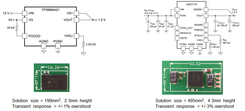
Appliances like power tools, garden tools and vacuum cleaners use low-voltage (two- to 10-cell) lithium-ion battery-powered motor drives. These tools use brushed DC (BDC) or three-phase brushless DC (BLDC) motors. BLDC motors are more efficient and have less maintenance, less noise and longer life spans.

The most important performance requirements of the power stage driving the motors are small form factor, high efficiency, good thermal performance, reliable protection and peak-current capability. A small form factor enables flexible mounting of the power stage inside the tool, better board layout performance and low-cost designs. High efficiency provides maximum battery life and reduces cooling efforts. Reliable operation and protection facilitate long lifetimes, which help with product reputations.

To drive a BDC motor in both the directions, you need to provide two half bridges (four metal-oxide semiconductor field-effect transistors (MOSFETs)) forming a full bridge. To drive a three phase BLDC motor, you need three half bridges (six MOSFETs) forming a three phase inverter.

With TI’s CSD88584Q5DC and CSD88599Q5DC power blocks, available in a small-outline no-lead (SON), 5mm-by-6mm package using a stacked die architecture, you can drive a BDC motor in both directions with just two power blocks and three-phase BLDC motor with just three power blocks , as shown in Figure 1. Each power block has two MOSFETs connected as a high side and low side MOSFET forming a half bridge.


Figure 1: Power block MOSFETs in different motor-drive topologies

Let’s look at the benefits that these power blocks could bring to a cordless tool motor-drive subsystem design.

Double the power density

The dual stacked die technology in the CSD885x power block enables twice as much silicon per printed circuit board (PCB) area, effectively decreasing the PCB footprint by 50% compared to discrete MOSFETs.

Compared to a discrete MOSFET of same performance level, which is available in 5mm –by-6mm, the power block integrating two FETs in the same package achieves PCB area savings of 90mm2 (3 x 5mm-by-6mm) for a three phase inverter topology. There will be MOSFET interconnecting tracks running in the PCB with discrete MOSFETs and a higher operating current ask for wider PCB tracks also, and hence the saving in PCB size is actually much more than 90mm2. Most cordless power tool applications use at least four-layer PCBs, with copper thickness more than 2oz. Therefore, saving in PCB size with power block leads to considerable savings in PCB cost.

Clean MOSFET switching with low parasitics

Figure 2 shows parasitic inductance and capacitances contributed by component leads and non-optimized layout in a power stage PCB design. These PCB parasitics cause voltage ringing and thus voltage stress on the MOSFETs.


Figure 2: Parasitic inductance and capacitance in a power stage half bridge.

One of the causes of ringing is diode reverse recovery. A high rate-of-change of current caused by fast switching can result in a high diode reverse-recovery current. The reverse-recovery current flows through the parasitic layout inductance. The resonant network formed by the FET capacitance and the parasitic inductance cause phase-node ringing, reducing the voltage margin and increasing stress on the device. Figure 3 shows phase-node voltage ringing with discrete MOSFETs as a result of circuit parasitics.

With power blocks, having the switch-node clip that connects the two MOSFETs keeps parasitic inductances between the high and low MOSFETs to an absolute minimum. The use of a low- and high-side FET in the same package minimizes PCB parasitics and reduces phase-node voltage ringing.

Using these power blocks helps to ensure smooth MOSFET switching without voltage overshoots even at currents as high as 50A, as shown in Figure 4.


Figure 3: Phase-node voltage ringing and voltage overshoot with discrete MOSFETs

Figure 4: Clean phase-node switching waveform with power blocks

Low PCB losses with reduced PCB parasitic resistance

The power blocks help to reduce the length of high current carrying tracks in the PCB and hence reduces the power loss in the tracks.

Let us understand the PCB track requirement in the case of discrete FETs. The PCB track connection between the top- and bottom-side discrete MOSFETs causes I2R losses in the PCB. Figure 5 shows the copper track when connecting the top and bottom discrete MOSFETs side by side; this is one of the common layouts for easy motor winding connection to PCB.  The copper area connecting the phase node has a length twice as the width (the track width depends on the current and the track width is normally limited by the board’s form factor). Alternatively, you could arrange the top- and bottom-side discrete MOSFETs up and down, keeping the phase node in between. But because of the need of provision to connect motor winding to the phase node, you may not be able to reduce the track length and also such an arrangement may not be suitable for all the applications.

If the design has a PCB copper thickness of 2oz (70µm), a single-layer PCB track connecting the phase node as given in figure 5, will have approximately 0.24mΩ resistance. Assuming that the track exists in two PCB planes, the equivalent PCB resistance is 0.12mΩ. For a three phase power stage, you have three such PCB tracks. You can perform a similar analysis for the DC supply incoming and return tracks also.

The power block, having the top side and bottom side MOSFET in single package and the phase node connected by a metallic clip inside the package, optimizes the parasitic resistances and gives you the flexibility for layout and saves a minimal 0.5 to 1mΩ total PCB resistance.

Figure 5: Typical phase-node track length with discrete MOSFETs

Superior thermal performance with dual cooling

The CSD885x power blocks come with DualCool™ packaging, which enables heatsinking at the top of the package in order to pull heat away from the board, offering superior thermal performance and increase the amount of power that can be dissipated in a 5mm-by-6mm package. As per datasheet specification, the power block has a junction-to-bottom case thermal resistance of 1.1°C/W and a junction-to-top case thermal resistance of 2.1°C/W. You can optimize the cooling either to the PCB from the bottom case or to the heat sink from the top case of the power block. Figure 6 shows the results with a top-side common heat sink (27mm-by-27mm-by-23mm) tested with three CSD88599Q5DC dual-cooled 60V power blocks in a 1kW,36V three phase inverter PCB (36mm-by-50mm), without any airflow. An electrically insulated thermal interface having low thermal impedance (Rθ < 0.5°C/W) is used between the heat sink and the power block top case during testing.

Figure 6: Thermal image of the board showing effective top-side cooling

In Figure 6, you can see the effectiveness of top-side cooling where the difference between the maximum temperature observed on the PCB (below the power block bottom case) and the heat sink temperature is less than 11°C. The heat is well conducted and distributed to the top-side heat sink through the top cooling metal pad of the power block.

Heat sharing between the top and bottom FETs

In a single- or three-phase inverter, the losses in the top- and bottom-side MOSFETs may differ. These losses normally depend on the type of pulse-width modulation topology and operating duty cycle. Different losses cause different heating of the top and bottom MOSFETs. When using discrete MOSFETs in a system design, you could try these different methods to equalize the temperature between the top and bottom FETs:

  • Use a different cooling area for the MOSFETs and provide more PCB copper area or heat sink for the MOSFET that has more losses.
  • Use different devices for the top- and bottom-side MOSFETs depending on their nominal current. For example, you can use a device with less ON state conduction resistance (RDS_ON) for the MOSFET that carries more current.

These methods will not give optimal cooling when the MOSFET heat up depends on the operating duty cycle, resulting in underutilization of the PCB area or MOSFET rating. Using power block MOSFETs, where the top and bottom MOSFETs are in the same package, results in automatic heat sharing between the top- and bottom-side MOSFETs and provides both better thermal performance and optimized system performance.

Low system cost

It is possible to optimize system cost by using power block MOSFETs in your design. The cost reduction will occur as a result of all of the benefits I’ve discussed in this post:

  • Half the solution size, reducing PCB cost drastically.
  • Low parasitics enable a much more reliable solution, one with longer life and low maintenance.
  • Reducing the PCB track length reduces the PCB resistance, resulting in lower losses and higher efficiency with a smaller heat sink.
  • Superior thermal performance resulting in less cooling efforts.

A MOSFET power block helps to achieve a more reliable, smaller-sized, efficient and cost-competitive system solution.

Additional resources

Viewing all 4543 articles
Browse latest View live


<script src="https://jsc.adskeeper.com/r/s/rssing.com.1596347.js" async> </script>