Quantcast
Channel: TI E2E support forums
Viewing all 4543 articles
Browse latest View live

Embedding more sensing and measurement at embedded world

$
0
0

Welcome to embedded world in Nuremberg, Germany. If you happen to be at the show, stop by and visit TI in Hall 3A, Booth No. 129 to see some really cool MSP430™ microcontroller (MCU) demos. If not, let me give you a glimpse of some of the sensing and measurement applications we’re highlighting.

At the show, we have our new MSP430 CapTIvate™ MCUs – the MSP430FR2522 and MSP430FR2512– which are optimized for cost-effective yet robust capacitive touch human machine interface (HMI) applications. (First two photos in the collage above.) You can also see the new MSP430FR6047 integrated ultrasonic-sensing flow-meter device, along with a wide variety of other TI products and designs. (Third photo in the collage above.)

In addition to our highly integrated, complex show demos, we wanted to see how quickly we could put together a simple demo using our available rapid prototyping hardware and software tools. We picked the low-cost MSP-EXP430FR2433 LaunchPad™ development kit for our project, and by using the Sidekick BoosterPack module to connect a solderless breadboard to the MSP-EXP430FR2433, the team was quickly able to connect a light sensor, indicator light-emitting diode (LED) and a simple transistor motor drive to the MSP430FR2433 MCU. (Fourth photo in the collage above.)

We chose the simple-to-use Energia integrated development environment (IDE) to develop code. The functionality of the code runs the motor for a set time frame when the light level reaches the threshold level, perhaps mimicking a simple control system to close an automatic window shade, or to dispense a predetermined amount of pet food. By using Energia, the team had the code up and running in a matter of minutes. Overall, this simple design was complete in under 30 minutes, and shows a great example of how quickly simple ideas can reach proof of concept by using the available MSP430 LaunchPad ecosystem.

The MSP430FR2433 value line MCU offers 16KB of embedded ferroelectric random access memory (FRAM) ultra-low-power nonvolatile memory; 4KB of static RAM (SRAM); a 10-bit, 200KSPS analog-to-digital converter (ADC) and multiple serial communication ports. The device is available in 24-pin very thin quad flat no-lead (VQFN) or die-size ball-grid array (DSBGA) packages.

Also check out our e-book, specifically written for MSP430 value line MCUs, which features 25 simple code examples to help you enhance board functions and jump-start your next project.


How to increase charging current by 50% with half the size in portable electronics

$
0
0

Modern portable electronic devices include a high-capacity lithium-ion battery to power the features we know and love, such as high-definition cameras, edge-to-edge high-resolution touchscreens and a high-speed data connection. As the list of features continues to increase, so does the battery capacity required to support them, along with the charge current required to recharge the battery in a reasonable amount of time.

One key consideration for system designers is balancing battery capacity, charging time and device temperature while charging. This last element is important, not only to enhance the user experience but to improve battery safety and lifetime. Given a battery’s capacity, you can reduce the charging time by increasing the charging current, while controlling the equipment temperature by reducing the total power loss inside the device.

Switch-mode battery-charger efficiency typically drops at higher current levels, which translates to a larger power loss and higher equipment temperatures. A buck-based battery charger can typically achieve higher efficiency by sacrificing solution size; for example, a larger inductor with a lower resistance might increase the efficiency of a typical design at high currents.

TI’s latest companion battery charger, the bq25910, is based on a three-level buck converter technology, which gives you the flexibility to increase efficiency by 5 percentage points while shrinking the solution size by 2x. This is an exceptional improvement in efficiency and solution size, and translates to a 50% increase in charge current for a fixed loss budget when compared to the older generation chargers.

The three-level buck converter illustrated in Figure 1 is a combination of a switched capacitor and switched inductor circuit with no fundamental duty-cycle limitation. With the addition of a flying capacitor, CFLY, balanced at VIN/2, the circuit reduces voltage stress on switching MOSFETs by half, doubles the effective switching frequency at VSW and reduces the volt-seconds across the inductor by half. The gate-driving scheme is similar to that of a two-phase buck converter. A complementary signal drives the outer FETs, QHSA and QLSA, with duty cycle D = VOUT/VIN. A second complementary signal of equal duty cycle drives the inner FETs, QHSB and QLSB, but is phase-shifted by 180 degrees.

Figure 1: The three-level buck converter circuit used in the bq25910 (a); the device’s total solution size is 56mm2, including all power components (b)

Assuming that CFLY remains balanced at VIN/2, the VSW node can be presented with three different voltages: VIN, VIN/2 and GND. The reduced voltage across the inductor dictates the ripple current in the circuit, which is a key parameter in selecting the required inductance. Because the inductor is typically the largest physical component of a switching converter, reducing its requirements translates to significant savings in solution size. This makes new applications possible such as height constrained, high charge current designs. Moreover, a smaller inductance will actually yield lower losses, hence the higher overall efficiency.

The addition of a flying capacitor allows the three-level buck converter to reduce switching losses in semiconductor devices as well as the size and loss of the external inductor, dramatically increasing efficiency. Even a small efficiency improvement can translate into a higher charge current, as explored by my colleague Fernando Lopez Dominguez in his blog post, “How 1.2% more efficiency can help you charge faster and cooler.” By improving efficiency by 5 percentage points, the bq25910 offers an increase in charge current from 2.9A to 4.35A for an equal power loss of 1.5W, all while reducing the total solution size 2x. You can see this illustrated in Figure 2, which compares the efficiency, size and temperature of the bq25910 to previous-generation chargers.

Figure 2: The bq25910 has +5% higher efficiency and +50% higher current for fixed losses (a); and runs 8°C cooler at half the size (b)

With each new generation, our portable electronic devices are becoming more feature-rich. These new features require both a larger battery capacity and a larger physical area to provide an enhanced user experience. This, in turn, places stringent requirements on battery chargers: they must occupy less space and charge a larger battery in an equal or shorter timeframe. The fact that typical buck converter-based chargers typically trade off efficiency for size requires a new technology that can provide both.

The bq25910 offers considerable improvements in fast and cool battery charging, all while reducing solution size. Consider taking advantage of this innovative solution in your next battery charger design with high current and high efficiency requirements. Order a bq25910 evaluation module today to enhance your next design with this truly innovative solution.

Additional resources

Accurate frost or ice detection based on capacitive sensing

$
0
0
The accumulation of frost or ice on an evaporator coil always presents a challenge in home appliances such as refrigerators, freezers and air conditioners. The accumulation of frost or ice insulates the air circulating through the evaporator unit, which...(read more)

Intelligently control an active clamp flyback

$
0
0

When I first got into cooking, I preferred to do it alone, thinking that having anyone else in the kitchen was a distraction. But as I started to cook more complicated recipes with multiple steps, I found that having a second pair of hands was invaluable and made the experience more fun. The saying is true: if you can’t beat them, join them.

The same principle applies with the active clamp flyback.

Everyone wants a smaller AC/DC converter, especially when it’s for their phone or tablet charger. Due to its simplicity, the flyback converter is the topology of choice, since it effectively converts AC to DC with few components. But there are limits to how small a flyback can be, since the losses associated with the leakage inductance of the transformer limit the practical size. Until now, every design has fought it by minimizing this leakage inductance.  But the active clamp flyback breaks this cycle.

Figure 1: Active clamp flyback with leakage inductance in red and active clamp in blue

Rather than fighting the leakage inductance by dissipating the energy in a resistor-capacitor-diode (RCD) or Zener clamp, an active clamp stores the energy and delivers it to the output. Intelligently controlling the clamp also provides zero voltage switching. This eliminates two major sources of loss, enabling the size to be drastically reduced. If you were to use gallium nitride (GaN) field-effect transistors (FETs) with their lower output capacitance and on-state resistance, the size of the adapter can be cut in half!

But the devil is in the details, since if the active clamp is not intelligently controlled, it will actually make the efficiency worse. The active clamp flyback had been only a pipe-dream, since there was no controller intelligent enough to enable this topology. But this has changed with the UCC28780. This active clamp flyback controller is specifically designed to work with silicon (Si)- or GaN-based power stages, making this topology a reality for any design. The UCC24612 synchronous rectifier enables compliance with U.S. Department of Energy (DoE) Level VI or Code of Conduct (CoC) Tier 2.

Additional resources

LIN: take a look inside

$
0
0

Did you know that drivers, passengers and even cargo can often benefit from up to 80 separate LIN modules placed throughout vehicles? These modules help implement a wide range of features that many of us use multiple times daily, without truly understanding what’s behind the button. Local Interconnect Network (LIN) adoption rates within automotive applications continue to rise as a low-cost and simple implementation for non-safety-critical applications when compared to the Controller Area Network bus standard (CAN).

Want to take a look inside one of today’s car models and see where you can employ LIN? Click the link below to launch an in-cabin virtual view and explore a few of the functions that LIN can enable today. Once the page launches, you can manually scroll and pan inside the vehicle and easily identify those locations where LIN is prevalent. Click the icons to obtain additional information, including block diagrams and reference designs, and accelerate your knowledge of LIN technology.

To take the 360 tour:

  • For best results and faster load time, ensure no browser tabs are open.
  • If you are having issues loading, try a different browser.
  • Click on the image below, and you will be taken to a landing page.
  • Use your cursor (click and hold it down) to pan around to see the entire lab.
  • You will find multiple interactive points explaining the LIN technology.

Additional resources

Maintain a constant phase margin in a synchronous buck converter

$
0
0

When designing a step-down buck converter, converter stability should be a top priority. The converter is stable when the phase margin of the loop gain is greater than 0 degrees, with an acceptable minimum phase margin of 45 degrees.  Maintaining a constant phase margin when the power-stage components vary as much as 50% from their original values can be a challenge for circuit designers.  For example, the values of the inductor and capacitors change with their bias operating conditions and temperature range.

Using the new advanced current mode (ACM) control topology in TI’s TPS543C20 synchronous step-down SWIFT™ converter, I compared the shape of the phase in three separate cases. In each case, I change the value of the output capacitor, inductor and both the output capacitor and inductor without making any other modifications to the circuit. I used the single-phase TPS543C20EVM-799 evaluation module (EVM) to perform the comparison under these test conditions:

  • Input voltage = 5V, output voltage = 0.9V, switching frequency = 500kHz.
  • Original inductor value = 470nH (0.165mΩ direct current resistance [DCR]).
  • Original output capacitor = 2 x 330µF (3mΩ equivalent series resistance [ESR]) + 3 x 100µF (1206 size ceramic capacitor).
  • Output load configured as a 10A resistive power resistor.

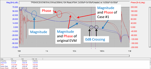
Case No. 1, illustrated in Figure 1

I compared the phase from the original default EVM to a new output capacitance value of 1 x 330µF (3mΩ ESR) + 3 x 100µF while keeping other conditions the same. As you can see, the shape of the phase very much stays the same as the original values. The phase is also basically staying constant over a decade of frequency after the double-pole frequency of inductor and output capacitor.

Figure 1: Bode plot comparison between original configurations versus case No. 1

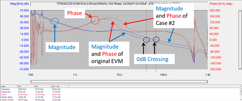
Case No. 2, illustrated in Figure 2

I compared the phase of the original default EVM to a new inductor value – 250nH (0.165mΩ DCR) – while keeping the other conditions the same. Again, the shape of the phase is very much the same as the default configuration. The phase is basically staying constant over a decade of frequency.

Figure 2: Bode plot comparison between original configurations versus case No. 2

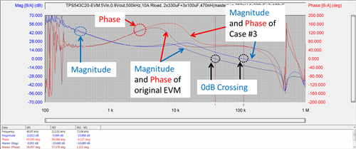
Case No. 3, illustrated in Figure 3

I compared the phase of the original default EVM to a combination of case Nos. 1 and 2 – 250nH (0.165mΩ DCR) and 1 x 330µF (3mΩ ESR) + 3 x 100µF – while keeping the other conditions the same. Again, the shape of the phase stays constant at 0dB.

Figure 3: Bode plot comparison between original configurations versus case No. 3

The shape of the phase in the ACM topology stays constant over a decade frequency range when the power component changes its value, such as a 53% inductor reduction from 470nH to 250nH.  However, you still need to pay attention to the changing value of power-stage components so that the phase margin of your converter meets the minimum requirement.

Additional resources:

GaN drivers – switching faster than today’s technology

$
0
0

It feels like we are living in a high-speed world, full of technology with a constantly growing demand for higher and faster performance.

Power engineers are at the forefront of this battle, developing solutions that are smaller, faster and more efficient than ever before. In applications like light detection and ranging (LIDAR), older-generation solutions only operated in hundreds of kilohertz. Newer platforms requiring longer ranges and increased accuracy need to be 10 times faster, with laser pulses below 5ns.

To achieve nontraditional performance, you need nontraditional technology. Only gallium nitride (GaN) can provide speed that fast with optimal performance. But to really harness the power of GaN, you need a driver capable of handling those frequency levels.

A very high switching frequency is necessary for next-generation telecom infrastructures like 5G envelope tracking, a key power method that ensures that the power amplifier is operating at peak efficiency during each point of transmission. Figure 1 shows losses from traditional supply-voltage methods compared to GaN-enabled envelope-tracking methods.

Figure 1. Traditional supply-voltage methods

TI’s Multi-Megahertz GaN Power Stage Design for High Speed DC/DC Converters, featuring the LMG1210 half-bridge GaN driver, enables 50MHz operation and optimized efficiency capability through adjustable dead-time control for the highest efficiency in 5G communication.

The driver’s ability to control dead time is a key design parameter in high-frequency converters, and is especially important as the frequency of operation increases. The device’s integrated dead-time control function allows you to fine-tune your design for best efficiency.

LIDAR is giving eyes to our technology, for detection, monitoring and mapping applications. But engineers need the fastest possible laser drivers to achieve high-resolution in LIDAR vision. The Nanosecond Laser Drive Reference Design for High Resolution LIDAR features the LMG1020 low-side driver; its 60MHz/ns performance provides sub-nanosecond pulses for the best performance in LIDAR laser applications. The increased power density in the industry’s smallest GaN driver enables extended range for industrial LIDAR vision, while short pulses comply with infrared (IR) laser eye safety standards.

5G envelope tracking, LIDAR, along with others, require excellent high-speed performance only enabled by GaN. TI’s GaN portfolio of products, including GaN drivers, gives you the speed to keep up with tomorrow’s technology.

Both the LMG1210 and LMG1020 are being shown at TI’s booth (No. 501) at the Applied Power Electronics Conference (APEC), March 4-8 in San Antonio, Texas. Find out more about TI GaN’s solution here.

Can you charge your EV faster?

$
0
0

There have been many announcements about rollouts of electric vehicles (EVs) across the globe. What makes these headlines exciting and different is the increasing capability of long-range driving beyond the current 200- to 300-mile range: These vehicles can now compete with internal combustion engine (ICE)-based vehicles across all driving situations and conditions.

Consumer acceptance is a key metric in making electric vehicles successful. Consumers aren’t concerned about EV prices, which they expect will drop given the falling price of lithium-ion batteries and short-term regulatory support across regions. They are concerned with increased charging speed/reduced charging time, however. After becoming accustomed to filling up their gas tank within a few minutes, do they have the patience to wait?

ICE vehicle fuel tanks take less than five minutes to fill up, whereas EVs take significantly longer to recharge their battery packs. This time frame is also compounded by a lack of charging stations, which means that consumers might even need to wait in line for their turn. I wrote a blog post about charging systems and their power levels that could potentially speed this up.

But what else can improve fast charging in a EV? Efficient power transfer, along with increasing power levels, is one way to improve charging speed both on- and off-board. Since batteries charge using a constant-current method to prevent damage, increasing the current is neither advantageous nor permissible based on regional restrictions. Increasing current can also cause wiring harness problems that in turn increase vehicle weight.

Increasing the voltage to 400V or greater is therefore considered a viable solution. Adopting wide-bandgap solutions for power electronics – namely silicon carbide (SiC) – efficiently transfers power at high voltages.

SiC is a wide bandgap semiconductor that has emerged as the disruptive material to replace silicon-based power switches (metal-oxide semiconductor field-effect transistors [MOSFETs] and insulated gate bipolar transistors [IGBTs]). Many automakers and charger suppliers are already implementing SiC because of its low losses (which improve efficiency) and ability to withstand high voltages. This  Implementing SiC as the power electronic switch is therefore becoming prominent with increasing battery voltages (400V and above) in BEVs and increasing power levels (>10kW) in onboard chargers and off-board DC chargers (50kW and above).

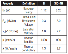
Low losses and high-voltage operation are possible because of SiC’s superior material properties, including low on-resistance, high thermal conductivity, high breakdown voltage and high saturation velocity when compared to silicon, as shown in Table 1.

Table 1: The intrinsic material properties of SiC

It is also important to understand how to drive SiC power devices. The controller dictates switch turn-on and turn-off for efficient power transfer across the power electronics circuit. A key element that acts as an interface between the controller and the power device is the gate driver, which acts like an amplifier that takes the controller signal and amplifies it to drive the power device.

Because of the superior characteristics of SiC FETs, defining gate-driver requirements becomes very critical – because these requirements differ than those for driving a silicon MOSFET or IGBT.

Learn more about TI SiC gate driver products that can efficiently drive SiC FETs by visiting ti.com/sic.

TI will be showcasing a full solar to vehicular charging ecosystem using SiC solutions at APEC 2018 in San Antonio. Discover more about the reference designs used in the demo:


Engineering leader and role model Cecelia Smith ignites a spark in tomorrow’s female engineers

$
0
0

Cecelia Smith thrives on the words “it can’t be done.” In our ongoing series, ‘One to Watch,’ we profile TIers who are making a difference through innovation or citizenship.

Since college, Cecelia Smith has been passionate about mentoring girls who love science.

“I love to see sparks of curiosity,” she said of her involvement in STEM education.  

Curiosity and a tendency to tinker with electronics early in life led Cecelia to her current role as vice president and general manager, leading a fast-growing business and global team of engineers developing, supporting and marketing one of our company's major power management product areas. She previously managed a key portion of our company's automotive product portfolio and continues to be a major advocate for automotive technology.

But while growing up in Paramount, Calif., she didn’t know a career in engineering was a possibility.

“When I was young, all I knew about engineers was that they drove trains,” she said.  “Engineering is not a topic that people in the neighborhoods where I grew up talk about. But there were some teachers in my life who made a difference. Without them, I wouldn’t be where I am today.”

Passion for problem-solving

Cecelia’s high school chemistry teacher was the first to open her eyes about the possibilities of a STEM career, sharing material on engineering coursework at California State University, where she later earned her bachelor’s degree.

Then, during an electronics lab course at the university, a professor noticed how much she enjoyed solving problems, working with test equipment and learning about circuit equations. He suggested that she explore a major in electrical engineering.

“That mentor gave information and direction to somebody who had passion and potential, but didn’t know where to place it,” she said. “He saw somebody who would make an electrical engineer.”

That pivotal moment set Cecelia’s course for a career doing what she loves: working with people to find solutions for tough problems and using creativity and vision to transform the impossible into the possible.

She joined our company in 1996 as a systems engineer and has held several positions developing strategies and product roadmaps and managing worldwide teams and customer relationships. She has been involved with the market creation and product development of several innovative technologies, including FireWire, digital amplifiers and digital audio processors.

“I thrive on the words ‘it can’t be done.’ This drives me to solve the unsolvable,” she said.

Her success is also driven by her composure, ability to listen and strong business acumen.

“She has a calm and sometimes-gentle exterior,” said Ellen Barker, our company’s chief information officer. “But she is an execution machine who drives for results and elevates her teams in the process.”

She builds strong relationships with customers while driving ownership and accountability throughout her organization, said Kyle Flessner, vice president in our manufacturing organization.

“Cecelia sets high expectations, executes through a strongly engaged team and collaborates effectively with other organizations,” he said.

Shifting mindsets

The qualities that make Cecelia a strong leader are helping build up a new generation of innovators and leaders at our company and in the technology industry. As chair of the TI Diversity Network’s global Women’s Initiative (WIN), she hopes to engage all TIers in a discussion about how to leverage individual differences to drive and fuel innovation.

“My biggest belief as a TIer is that different perspectives develop and strengthen good ideas into great ideas,” she said. “WIN brings women together from across the world and encourages them to fully participate and thrive in all areas of TI’s business, and that benefits both women and men and ultimately makes our company a great place to work for everyone.”

She helps elevate the voice of women TIers in a different way, said Fran Dillard, diversity and inclusion director. As one of our company’s senior leaders, Cecelia has an experience level that can shift mindsets.

“Cecelia has a unique understanding of opportunities where we can help women be better prepared for key technology roles and for leadership,” Fran said. “She knows what senior leaders are looking for, and she can bring that back to women in ways that maybe they haven’t heard before.”

Leading by example

Cecelia believes that showing girls what it looks like to be an engineer is the most powerful way to cultivate the next generation of female leaders.

In college, she mentored students one-on-one at nearby high schools and tutored them in math and science. Once she began her career, she shared her story to larger groups – ranging from middle school students to college-aged audiences – offering the advice she would give to her younger self.   

“One piece of advice I always give is that you’re in charge of your career, your continuous development and your life,” she said.

The challenge, she says, is finding the time to volunteer.

“The only way to tap into talents and passions is to be a role model,” she said. “We need to show the next generation that there are people like themselves who are working in the field – and to show them that engineering is changing the world.”

How to create a robust building security system with TI’s new SimpleLink MCU platform

$
0
0

It’s hard to imagine a world before smartphones. What used to be a futuristic plot on the Jetson’s is now the reality we live in. As we strive to connect more of our lives, homes and buildings, the design complexities can rapidly escalate. Learning wireless protocols and acquiring radio-frequency (RF) design experience can be an overwhelming venture. Add network security and power budgets into the mix, and you’ll quickly feel like a freshman walking into their first college lecture.

Take a home or building security system as an example. There are door and window sensors, motion detectors, smoke detectors, smart locks, and a security panel that need to connect wirelessly, comply with local regulatory requirements and perform with high accuracy at the lowest power consumption. That’s a big task to execute. But I have a few simple pointers that can help you avoid the headache and design with ease.

1. Select a platform that supports multiple wireless protocols.

A building security system may have multiple RF technologies and will often leverage multiple protocols. These are the leading players for building security applications:

  • Sub 1-GHz is a dominant technology for any security sensor because of its extremely long range capabilities and great wall penetration for indoor applications. You can use this protocol to create a low-power star network of sensors that report data to a gateway or collector.
  • Zigbee® is a great technology for device-to-device communication, as it is a proven solution for a mesh network. It’s popular in electronic smart locks, door and window sensors, and smoke detectors, with well-defined security procedures to protect data.
  • Bluetooth® low energy is an emerging technology that’s often used in conjunction with Sub 1-GHz or Zigbee. Bluetooth low energy’s inherent smartphone connectivity makes it a great choice for configuring a network and diagnostic alerts. With the range enhancements of Bluetooth 5, this low-power protocol is also a good fit for battery-operated sensors within a home or for appliances such as electronic smart locks.
  • Thread is also an emergent technology designed to control and connect products such as motion sensors, gas detectors or gateways. Thread uses the 2.4GHz industrial, scientific and medical (ISM) band to create a secure mesh network and is based on Internet Protocol version 6 (IPv6), giving it a natural connection to existing networks. Thread supports device-to-device, device-to-smartphone, and device-to-cloud communication, which makes it easy to use and extremely scalable.

You can implement building security systems using any one of these technologies or a combination of several of them. Thus, it’s a good idea to choose a hardware platform that can address multiple protocols and give you software flexibility depending on your application.

2. Address network security.

Security is a key concern, especially in building security systems. Consumers want to know that their personal information will remain protected. When choosing a wireless platform, security must be at the forefront of your decision. Let’s take a look at the security measures of the wireless protocols I just reviewed:

  • In Sub 1-GHz, designers can implement the Advanced Encryption Standard (AES) algorithm and authentication, as well as message integrity to ensure network security.
  • Bluetooth low energy also leverages AES hardware encryption. The Bluetooth low energy 4.2 specification implemented increased security to prevent man-in-the-middle attacks and correct pairing vulnerabilities.
  • Zigbee has defined procedures to ensure the secure request and exchange of keys, and uses install codes to eliminate the use of well-known keys as well as AES encryption.
  • Thread implements IP-based security with Datagram Transport Layer Security (DTLS), password-based authentication and AES encryption.

With each of these protocols, it’s important to assess the threats in your system and use security enablers to address these concerns.

3. Seek high performance and low power.

When designing a building security system, you have to take range and power seriously. Extending the battery life of door and window sensors, electronic smart locks, and smoke detectors helps create a positive experience with the end product. Not only do you have to evaluate a device’s receiver and transmitter current; you must also evaluate the sleep current to ensure maximum battery life.

Likewise, ensuring maximum coverage within a home is paramount. Whether it’s controlling a large number of devices within a mesh network or simply using a smartphone to control one device, it’s imperative that users can maintain a reliable connection. Output power and sensitivity are the critical parameters you need to determine the achievable range. By leveraging a large link budget, a security system will be able to cover a greater distance within a home or building.

Conclusion

Designing a security system can be challenging, especially when it comes to the many connectivity options, network security, and performance. With the flexibility to support Sub 1-GHz, Bluetooth low energy, Zigbee, Thread and dual-band protocols, TI’s next-generation wireless microcontrollers (MCUs) are geared to provide robust and secure solutions for building security systems (Figure 1).

Figure 1: SimpleLink next-generation wireless MCUs

These powerful devices feature more memory, peripherals, flexibility and processing power, as well as excellent RF performance at extremely low power consumption. As you design a building security system, keep the suggestions above in mind to unlock the most innovative designs yet.

Additional resources

Delivering power to the industrial market with Ethernet

$
0
0
Powering industrial Ethernet devices requires addressing specific aspects of industrial Ethernet and industrial applications. The biggest difference between standard Ethernet and industrial Ethernet is the topology, as shown in Figure 1. Standard Ethernet...(read more)

Measuring efficiency, the right way

$
0
0

Efficiency is the most crucial criteria for some power supplies. With high-efficiency controllers like the UCC28780, it is important now more than ever to understand how to conduct a proper efficiency measurement that adheres to regulation standards. In this post, I’ll show you how to properly connect and measure AC/DC power supply efficiency.

Proper test conditions:

Efficiency measurements are only as good as the connections from which they’re made. To make efficiency measurements as accurate as possible the first step is to make sure that no unnecessary equipment/circuitry is connected to the board, such as an oscilloscope connector or other meters that are not needed in the efficiency measurement test itself. If there are connections that draw power that cannot be removed, their power consumption needs to be noted in the measurement or calculation and not neglected. This is critical in low-load and stand-by power, in which any external connections will have a larger impact in the efficiency measurement.

The next step is to place the probes for measurement. One option is to put the probes as close to the output as possible, like on the output capacitor or at the pins of jumper J6 in the UCC28780 evaluation module (EVM), as shown in Figure 1. However, if the power supply has a fixed cable, you should measure from the end of the fixed cable rather than directly from the output. Connecting this way ensures a proper Kelvin connection and provides high-accuracy measurements. 

Figure 1: UCC28780EVM connection diagram for efficiency measurements

Now let’s move to the input side of efficiency measurements for AC/DC converters. A dedicated power meter is required, as the two-multimeter setup used on the output side would not be accurate for the input because the multi-meters would not account for the harmonic content like a power meter would. Similar to the output, your goal is still to place the measuring probes as close as possible to the board’s input. Both input and output connections are shown in Figure 2, and match the color scheme of Figure 1.  

Figure 2: Probe connections for efficiency measurements

Proper testing procedure:

Title 10 Electronic Code of Federal Regulations outlines the correct way to conduct power-supply efficiency measurements, and will be linked in the additional resources. Here are the steps for performing an accurate efficiency measurement:

  • Turn on an AC source with a high line voltage (230AC/50Hz for Europe or 115AC/60Hz for U.S.A) and with a 100% load. Let the device under test operate for at least 30 minutes to ensure that the board is warmed up and stable for measurements.
    • The unit under test is considered stable if the AC input power does not deviate/drift more than 5% from the maximum power value observed.
    • If the AC input power is not stable after five minutes, continue to monitor the input power in five-minute periods until the reading is stable.
  • After the initial warm up period, take the first measurement at a 100% load. Use an AC power meter to monitor the input power for a period of five minutes before assessing the stability of the power supply.
  • The remaining load conditions are 75%, 50%, 25%, 10% and 0% load, in that order. You only need one warm up time of 30 minutes, so these subsequent measurements only need a minimum of five minutes to become stable enough to record measurements.

A test procedure would then look like this:

  1. Warm up the unit under test for 30 minutes under a full load, 230VAC/50Hz or 115VAC/60Hz.
  2. Assess the stability of the unit and take measurements if stable.
    1. If not stable, continue to monitor output until stable.
    2. Drop load to 75%; monitor for five minutes to assess stability then take measurement.
    3. Drop load to 50%; monitor for five minutes to assess stability then take measurement.
    4. Drop load to 25%; monitor for five minutes to assess stability then take measurement.
    5. Drop load to 10%; monitor for five minutes to assess stability then take measurement.
    6. Drop load to 0%; monitor for five minutes to assess stability then take measurement.

Figure 3 outlines the test procedure in a flowchart diagram.

Figure 3 Efficiency measurement procedure

Conclusion:

Engineers can test things many ways. As the industry continues to push for higher and higher efficiencies in power supplies, it is important to have a good grasp on what a consistent testing environment and procedure look like. 

Solving voltage transient challenges with an integrated buck-boost converter

$
0
0

Automotive body electronics and gateway modules must operate without interruption, regardless of variations in the car battery. A car’s battery voltage can drop down to below 3V during cold crank and may surge as high as 40V during load dump, thus necessitating a DC/DC power supply to both step up and step down and maintain a regulated operating voltage from 5V to 12V.

In addition, DC/DC power supplies should have a small solution size in order to save space, operate with low quiescent current for minimal drainage of the car battery, and be capable of 2MHz switching to avoid electromagnetic interference (EMI) in the AM band. In this blog post, I will compare typical conventional DC/DC power-supply solutions and examine the advantages offered by integrated wide input voltage (VIN) buck-boost converters.

Conventional solutions

In order to produce the regulated voltage of 5V or 12V, the DC/DC power supply should be able to boost up the battery voltage from as low as 3V during cranking and buck down the battery voltage when it is higher than the required output voltage.

Figures 1 through 4 show simplified power architectures of the conventional solutions. For presentation simplicity, these figures use diodes as the rectifiers, but you can replace them with power metal-oxide semiconductor field-effect transistors (MOSFETs) for higher power-conversion efficiency.

Figures 1 and 2 offer straightforward and quick solutions by cascading two power stages, using one buck and one boost. You can save development time when both the buck and boost stages are existing designs. A main drawback is the low efficiency caused by the two conversion stages. For instance, even if each stage can achieve 90% efficiency, the overall efficiency is the product of the two, yielding 81%. Another drawback is the relatively higher bill-of-materials (BOM) cost and larger solution size – owing to the use of two power inductors, two controllers and more peripheral components, which may duplicate some functions of the two controllers.

Figure 3 shows a single-ended primary-inductor converter (SEPIC) converter, achieving the power conversion in a single stage. However, it still requires two inductors. Although you can use coupled inductors to replace two separate ones, the former undoubtedly costs more than the latter. The AC coupling capacitor that the SEPIC requires also adds to the BOM cost.

Figure 4 shows a buck-boost converter. It is a single-stage converter and only needs one power inductor. The nonsynchronous rectifier reduces overall efficiency.

Figure 1: Conventional architecture No. 1: pre-boost followed by buck


Figure 2: Conventional architecture No. 2: buck followed by post-boost


Figure 3: Conventional architecture No. 3: SEPIC


Figure 4: Conventional architecture No. 4: buck-boost

Using the synchronous rectifiers as shown in Figure 5 improves the efficiency, but four external MOSFETs raises the BOM cost. There are also challenges associated with difficulty in the printed circuit board (PCB) layout and the routing of power components for optimal performance.

Figure 5: Synchronous buck-boost

Highly integrated wide VIN buck-boost converters

A buck-boost converter with all four power MOSFETs integrated with the controller overcomes the drawbacks of conventional solutions. Figure 6 is a simplified block diagram of an integrated buck-boost converter. Typical products include TI’s TPIC74100-Q1, TPS55060-Q1 and the recently released TPS5516x-Q1 family. These products support a maximum load of up to 1A in a miniature solution size.

Figure 6: Integrated single-stage single-inductor solution: buck-boost converter

An application example

Figure 7 shows a typical solution with the TPS55165-Q1 for 5V at 1A applications. The full solution requires less than a dozen external components.

Figure 8 shows the miniature solution size. For reference, the integrated circuit (IC) size is 6.5mm by 4.5mm. It’s possible to further reduce the solution size for double side mounting.

Figure 9 shows the circuit’s performance under cold cranking. You can see that the output voltage is solidly regulated at 5V even during transient conditions.

Figure 7: A complete solution with the TPS55165-Q1 for a 5V/1A application


Figure 9: Battery voltage cranking response (conditions: IOUT = 0.5A, VIN transient: 12V to 4V)

Conclusion

Four-switch buck-boost converters are optimal for automotive applications by using a single conversion stage, a single power inductor and a minimal number of external components. With 2.2MHz frequency switching, 15µA low IQ operation, optional spread-spectrum technique and a miniature solution size, the highly integrated wide VIN TPS5516x-Q1 family is a good fit for body control and gateway modules.

Check out the product pages for the TPS55160-Q1, TPS55162-Q1 and TPS55165-Q1, where you can also find the links to the data sheets, EVMs, Pspice models and the WEBENCH® online simulator. Questions? Post them to TI’s E2E community.


New technology charges your smartphone in just 30 minutes

$
0
0

Focused on success
The project to create a higher current battery charger began several years ago. As consumers around the world increased their reliance on smartphones for connectivity and productivity, their desire for ever-faster charging times grew. At the same time, new models of phones got slimmer, so the space available for batteries also kept shrinking.

A team from Kilby Labs, which is our applied-research center, and our battery-management team developed innovative technology that doubles the power density, provides high efficiency, simplifies designs and reduces thermal loss in batteries.

The latest release is the bq25910, the first 6-A, three-level buck battery charger. The core of the device’s lightning-fast charging is a new three-level power-conversion technology never before productized for this application.

“The bq25910 epitomizes our company’s approach to thermal management challenges,” Jinrong said. “We continually strive to deliver battery-management devices that provide faster, cooler charging in all types of portable electronics.”

How to Select a MOSFET – Battery Protection

$
0
0

In the fifth post of this series, I discussed some considerations for selecting a MOSFET for use as a load switch, specifically for small-signal applications. In this post, we will look at a very similar function in which a MOSFET is used for battery protection.

Every year, more electronic devices are powered by batteries comprising Lithium ion (Li ion) cells. . The high power density, low rate of self-discharge and ease of recharging have made them the preferred battery type for nearly all portable electronics – Nowadays, everything from the cell phone in your pocket to the electric cars millions drive to work on a daily basis are powered by Li ion batteries.. Despite their many advantages, these batteries also pose certain risks and design challenges that when not successfully mitigated can lead to catastrophic results. I don’t think anyone will soon forget the exploding Galaxy S7 devices tablets and subsequent recall in 2016.

A common way to mitigate the risk of this type of destructive event is to place MOSFETs in the charge and discharge paths that can sever the electrical connection between the battery and the rest of the electronics in the end circuit when the battery voltage is considered outside a designated safe range, or the IC detects an overcurrent surge during charging or discharging. In essence, the MOSFET serves as an electronic fuse (E-fuse) (see Figure 1).

Figure 1: Simplified single-cell Li-ion battery-protection circuit

Because this is not a fast switching application, once again you really only have to contemplate worst-case scenario conduction losses, which make the selection criteria of the MOSFET similar to that of the load switch. But there are some unique considerations that warrant a separate discussion to highlight those caveats that are specific to battery protection.

Because a battery-protection MOSFET is both fully enhanced and continuously conducting current, or entirely shut off to disconnect the battery voltage from the rest of the electronics, you can pretty much neglect switching parameters when considering FETs for this application. Instead, just like when selecting load-switch FETs based on their current-handling capability, resistance and package type are the two most important considerations. With this in mind, it makes sense to break down battery protection into three tiers of currents that different types of end equipment require and analyze the type of FETs used for each.

In the first tier are low-power personal electronics that run on one to two battery cells, like cellphones, tablets, smart watches or personal health trackers. The amount of current these devices consume while charging and discharging can be as high as a few amps or as low as a few hundred milliamps. It’s no secret that personal electronics designers are perpetually driving to reduce their product’s size (and weight) with every passing generation, so they select FETs for battery protection based on the criteria that they be as small as possible while still being capable of handling the maximum charge and discharge currents. Sometimes this means a chip-scale device like a FemtoFET™ N-channel MOSFET is a good choice.

Because the FETs are often placed back to back in these applications, blocking both the charge and discharge paths (as in Figure 1 above), sometimes integrating both devices into a single package in a common drain configuration is the most space efficient solution (Figure 2). TI has a number of integrated back to back devices, available both in chip-scale packages as well as small quad-flat no-lead (QFN) SON3x3 plastic packages.

Figure 2: Schematic for a common drain-configured FET integrated into a single package

The second tier of battery-powered devices are multicell handheld cordless power tools like drills, trimmers, small saws and home appliances like robotic vacuum cleaners. These devices can still be sensitive to size, but charge their batteries at considerably higher currents, generally above 10A. As such, designers generally use the lowest resistance D2PAK, TO-220 or in some cases QFN packages. It is possible, when necessary, to use multiple devices in parallel, particularly for larger tools like chainsaws and hedge trimmers,  but keeping the number of FETs to a minimum in order to maintain a small form factor is still important. Like motor-control FETs, the lowest resistance device in a given package is generally preferable; otherwise you would select a smaller package.

The third tier highest-power battery-charged applications – are electronic vehicles like e-bikes, e-scooters, even electric cars and busses. At this point, the current and power levels can be massive (hundreds of amps, several kilowatts of power), and there really is no way around paralleling multiple FETs for the charge and discharge path. I’ve seen designers parallel dozens of FETs on massive boards, usually using D2PAKs, heat-sink-mounted TO-220s or other thermally enhanced packaged devices (Figure 3). Except for smaller-design e-bikes, size is less often an issue and current-handling capability is the name of the game. Once again, this means selecting only the lowest-resistance FETs. The number of FETs required is a function of the resistance, the maximum ambient temperature, and the thermal impedance of the board and system as a hole. While back-of-the-hand calculations can get you in the ballpark, precisely nailing down the number of FETs required will usually require some rigorous thermal simulations.

Figure 3: Dozens of D2PAK FETs paralleled on a large PCB for charge and discharge of the battery of an electronic vehicle

One last note on the use of battery-protection FETs in electronic vehicles –it is critical that you determine whether the end application requires Q101-grade FETs. Q101 is the automotive qualification grade from the Automotive Electronics Council (the discrete equivalent of Q100 for integrated circuits) that imposes much harsher quality and reliability requirements than are mandatory for commercial-grade devices. Whether your devices require Q-101 certification depends on the end application and a number of other factors, from the customer’s standards to the legislation of the country in which the vehicle will be operated.

E-bikes and e-scooters are generally less likely to require Q-101, but this is not always the case. Better to find this out before you build your design around FETs that you can’t put inside the final end equipment. TI does not offer any automotive-qualified FETs in its portfolio so if this is a requirement, your FET solution will have to come from elsewhere.

Thanks for reading! In my next and final blog in this series, we will be discussing the selection process for MOSFETs that are used for Hot Swap and other similar applications. 


Designing for a scalable metering platform

$
0
0

Everywhere you look, you can find references to “smart” things – smartphones, smart TVs, smart homes and even smart cities. The intelligence of the devices that surround us continues to increase, and perhaps that intelligence is most important in the utility systems that sustain our cities. The world’s electricity grids in particular are undergoing a revolution in the control systems that connect generating plants to factories, businesses and homes. What was once a network of electromechanical systems is becoming much more highly automated and driven by ever-more-intelligent devices. These devices form a smarter electric grid that supports a number of trends: from centralized to distributed energy generation; from unidirectional to bidirectional information flow; and from traditional, constant power generation to a variety of renewable generation sources that may change over time.

These smart-grid trends bring improved connectivity, improved robustness in the face of shifting energy demand and greater overall energy efficiency. Microcontrollers (MCUs) are at the core of many devices – such as data collection gateways, fault indicators, remote terminal units and smart meters – that are central to the smart grid.

In this post, I’ll discuss four important attributes of an MCU in smart grid/smart metering applications.

Large integrated memory

Added intelligence in a metering device means more complexity, more intelligence and more code. The smart grid uses a greater number of wired and wireless communication standards than traditional electric grids, and those standards will change over time while new ones emerge. These conditions drive the need for a large amount of integrated flash storage, both to hold multiple communication stacks and to have the memory needed to support secure, reliable updates on a smart meter host. Over time, wired and wireless communication standard requirements are likely to increase, which means that your choice of MCU should include a platform that allows your design to scale.

Low-power operation

As power sources become more varied, the supply of electricity may no longer be constant in some locations. Supporting a resilient grid requires low-power devices that can operate for as long as possible, even during power outages, to maintain control and communication. Low power is even more of a concern for nonelectric meters such as gas or water-flow battery-powered meters, whose life expectancy can be 10 or more years.

Accurate sensing and measurement

In a smart meter, the MCU is the hub responsible for collecting usage data and reporting it to upstream control nodes. Accurate sensing in the form of precision analog-to-digital (ADC) conversion coupled with higher sampling rates is needed to correctly measure energy or other utility usage. Low-power usage is important here too, since it allows higher sample rates and a more precise picture of utility usage without sacrificing battery life.

Unified development platform

Developing systems for the smart metering infrastructure requires the use of multiple MCUs to provide wired or wireless communications as well as metrology and host functions. A unified environment can enable fast and efficient development of new applications by providing validated and documented drivers, communication stacks and code examples. Building a system this way enables easy reuse of application code as the system scales to include more wireless protocols (such as Sub-1 GHz, 2.4GHz and dual-band solutions) or expands to include stack solutions (like Wireless M-Bus, Zigbee, Thread, 6LoWPAN, Bluetooth® low energy or other proprietary solutions).

SimpleLink™ MSP432™ MCUs

To meet the evolving needs of smart grid devices and more intelligent utility meters, TI has developed the SimpleLink MSP432 line of MCUs. This family offers low-power operation with large flash memory options of 512kB, 1MB or even 2MB. The MCUs contain integrated peripherals targeted at the needs of the smart-grid infrastructure, including a precision low-noise, low-power ADC and a low-power liquid crystal display (LCD) controller. See Figure 1 below for an example of how you can start building your smart meter with the MSP432P4 host MCU.


Figure 1: Setup for a smart meter with an MSP432 MCU


All features tie together with the SimpleLink software development kit (SDK), which enables a developer’s investment in one device to carry over into the entire product family of SimpleLink wired and wireless MCUs.

Additional resources

Would you like a logo to go with your PoE system?

$
0
0

In order to reach their true potential, all “standards-based” solutions such as USB and Underwriters Laboratories (UL) require an easy way to identify compliant solutions. Otherwise, a promising solution is held back over confusion and/or fear about what is really inside the box. Is it “as promoted” on the data sheet? How can you be sure? And what do you do when real-life experiences result in questioning the standard itself?

Such was the case for Power over Ethernet (PoE) – until Jan. 16, 2018.

Following a worldwide press release by the Ethernet Alliance (EA), PoE technology enters a new era in ease of adoption by providing an easy way for end users (or anyone in between) to determine if a design is compliant to the current standard – and at what power level. The new certification program also allows for faster debugging/troubleshooting when PoE systems are demonstrating interoperability issues between the PSE and PD ends of the CAT-5 cable.

As Figure 1 shows, there are essentially two categories of certification marks: one for use with powered devices (PDs), also known as “loads,” and one for power sourcing equipment (PSE), also known as “power sources.” The arrows indicate the directional flow of current in the system. In the case of PDs, the arrow points into the logo, indicating that the equipment is capable of receiving power. In the case of PSEs, the arrow points out from the logo, indicating the equipment is capable of sending power. The number inside the boxes indicate the class level certification granted (see Table 1). For those unfamiliar with PoE, these numbers directly correspond to the maximum power a PoE-enabled design can send or receive.

Figure 1: EA certification marks (logos)*


Table 1: PoE class levels

This initial rollout was limited in scope to the current Institute of Electrical and Electronics Engineers (IEEE) 802.3 standard (and to classes 1-4), but work is well underway to define the test suite for verifying future designs under the planned IEEE802.3bt standard (which will add classes 5-8).

TI believes that end equipment with a PoE logo provide a competitive advantage and we want to enable our customers to achieve this.  TI is putting our popular EVMs and Reference Designs through EA certification so that end equipment design engineers can start from a verified solution and have higher confidence that their design will pass industry compliance testing.


Start your new PoE design with increased confidence by looking for the logo.

* EA CERTIFIED & PD Mark™ and EA CERTIFIED & PSE Mark™ and EA CERTIFIED™ are certification marks of The Ethernet Alliance in the United States and other countries. Used here under license. Unauthorized use strictly prohibited.


Additional resources


Does your design have a low talker?

$
0
0

Many of you can relate to having a conversation with a “low talker” – someone whose ultra-low voice makes them difficult to understand. Communicating with a low talker often leads to miscommunication and mixed signals, illustrated to great effect in a well-known sitcom from the 1990s.

So what does a low talker have to do with electronic systems and their designs? Modern electronic signal chains are starting to incorporate more integrated circuits (ICs) that operate at lower voltage nodes. Sub-1V devices such as large microprocessors, field-programmable gate arrays (FPGAs), low-power communication devices and sensors are just a few of the types of devices that are moving to sub-1V levels in order to reduce power and extend battery life. Lower voltages for these devices also means that their input/output (I/O) data interfaces need to operate at lower voltages. In effect, these new low-voltage signal-chain devices are becoming the system’s low talkers.

Just as it can be frustrating to understand low talkers, device-level low talkers present a problem to other devices in the system’s signal chain. The data interfaces of low-voltage devices may not be able to interoperate with higher-voltage devices, resulting in data-signaling issues that you will need to address for proper system operation.

The solution is a voltage level translator that can understand low-voltage devices and translate the data to higher-voltage devices. The concept of I/O level translation has been around for quite some time, with engineers using both discrete as well as integrated IC-based solutions to implement level-translation schemes. Using discrete level-translation solutions to shift between a low talker device I/O and a higher I/O voltage device requires multiple components such as transistors and resistors, carefully selected to ensure proper operation over temperature.

As voltages move lower, discrete approaches are likely to take more engineering effort while remaining inflexible to system voltage variations. Integrated level-translation solutions (IC devices) have been available for quite some time to support level translation for devices operating between 1.2V and 5.5V and provide the flexibility system designers need. However, the older generation of integrated level translators will not be able to support the needs of systems based on new ultra-low-voltage processors, FPGAs, microcontrollers (MCUs) and sensors that have an I/O voltage <1V.

As market necessities such as longer battery life and energy efficiency drive system component voltages lower, a new class of integrated level-translation solutions will be necessary to communicate with a system’s low talkers. Building on our large portfolio of level-translation solutions and long history of logic development, TI is helping system designers overcome the challenges associated with decreasing I/O voltages. Our latest direction-controlled voltage level-translation devices enable system designers to support I/O voltages of <0.80V.

The SN74AXC8T245, an 8-bit direction-controlled voltage translator, and the SN74AXC1T45, a 1-bit direction-controlled voltage translator,  are the first devices in a new family of voltage translators developed to enable designers to implement robust next-generation low voltage interfaces within their systems.   Both the SN74AXC8T245 and SN74AXC1T45 are available in multiple package options making them suitable for many different application spaces.

Figure 1: Example of low-voltage level translation

This new family can help solve low-voltage level-translation problems often encountered by design engineers. For example, low-voltage translation often means that you have to compromise on the amount of current drive that you can expect from the level translator. The new family of devices are compliant to the Joint Electron Devices Engineering Council (JEDEC) 0.7V standard (JESD8-14A.01), which means that these level translators will source enough current to meet common I/O standards, unlike most level-translation devices in the industry.

In addition, the new voltage translators consume much lower power than competing level-translation devices available today. For example, the SN74AXC1T45 will have 60% lower power dissipation than competing devices on a per bit basis, which is extremely beneficial for battery-operated and power-sensitive applications.

System designers are likely to see low talker devices in their designs more frequently in the coming years as system voltages move lower. When you encounter low talker devices in your designs, avoid embarrassing design issues by using level-translation solutions designed to put low talkers in their place.

Additional resources

Trash becomes treasure as TI volunteers use recycled plastic waste to build an eco-park

$
0
0

From trash to treasure - transforming plastic bottles into a park for elementary students
On a recent Saturday in Baguio City, Philippines, volunteers from our company and their family members headed to a nearby eco-park. But the outing was no company picnic.

They went to complete the final stage of a year-long project to transform a trash dump into a park.

Situated behind Bonifacio Elementary School, the park is a new place for students to play, plant flowers and vegetables, and learn about ecology and entrepreneurship. But this isn’t a typical park – it’s built with plastic eco-bricks that were collected by TIers.

An eco-park is brought to lifeOver the past year, our employees contributed more than 2,000 1.5-liter plastic bottles, each jam-packed with non-biodegradable pieces of plastic waste. With help from families, friends and neighbors, TIers spent thousands of hours in their spare time collecting and filling the clear and green-tinted vessels with chopped-up plastic shopping bags, plastic packaging waste, and other down-cycled bits to create solid, heavy eco-bricks.

At the school, parents and other community volunteers began cementing the plastic bricks in place in December to pave pathways, create plant boxes and build stairs in the hilly terrain. On this recent February weekend, volunteers put the finishing touches on the park by constructing an eco-brick stairway to the park.

A heartbreaking problem and an eco-friendly answer

Saving and stuffing 2,000 empty soda bottles did more than just keep 4 tons of trash out of landfills and off the beaches. Nicole Dela Cruz, an engineer at our company who spearheaded the effort, said the project raised awareness about the world's plastic-waste problem, which she called especially heartbreaking in the Philippines.

"The Philippines is an archipelago of 7,100 islands in the Pacific Ocean. We see the difference when we dispose of plastic properly," she said. "Instead of continuously throwing away plastic, the message is to be more conscious of how we use and dispose of it."

A heartbreaking problem and an eco-friendly answer The Baguio elementary school isn't the first place to benefit from an eco-brick construction project. Inspiration for the project came from an article Nicole read in late 2016 about how budget-challenged communities in Africa, Central America and elsewhere in Asia were repurposing their plastic waste this way. To erect sturdy structures, builders lined up the stuffed bottles horizontally and covered them with cement, or they placed them into a basic support structure and framed them with wire mesh and bamboo. Nicole saw an opportunity to repurpose our company’s own castoff materials the same way.

She pitched the idea to members of Baguio’s Community Involvement Team, who agreed it could have a big impact. In February 2017, the team set up collection boxes around campus and launched a factory-wide #StuffItChallenge campaign to round up 2,000 eco-bricks. On weekends, they collected plastic industrial waste and organized fun events where talented TIers performed small concerts for colleagues as they filled bottles together.

An eco-park is brought to life

The program also promoted camaraderie, said Sandy Paguio, communications manager for the company in the Philippines. "The events got larger as people brought friends and their whole families. People from outside TI would say what a nice initiative it was, and we heard stories about TIers who would go out on their streets collecting waste. Then their neighbors would start collecting and stuffing bottles themselves."

Nicole explained: "The goal was to convey the message that, because plastic is going to be around forever, we should be reducing the amount of plastic we're using and doing something with the plastic we can't avoid using."

She and her team identified potential projects that could put the eco-bricks to good use, and the nearby school, which several TIers once attended, became the first beneficiary. Bonifacio Elementary School was already building eco-brick bleachers for its basketball court, and Principal Margie Estoesta dreamed of adding an eco-park for students. "She lacked the budget for materials. It was the perfect partnership," Nicole said.

Looking to the future, volunteers are eyeing an opportunity to construct a retaining wall at another school in a remote, hilly area. "We need to start collecting eco-bricks again," Nicole said. “They are already getting requests to set-up donation boxes to collect the eco-bricks that TIers have continued to make from home.”

How to select the right USB Type-C™ signal switches

$
0
0

USB Type-C™ enables the transfer of data, video and power over a single cable and connector. The flip-ability of the USB Type-C connector introduces connection pin redundancy, which requires a signal switch in order to bring the correct data path to the central processing unit (CPU) for signal processing.

There are two types of signal switches: USB only and USB plus video. Figure 1 shows USB-only switches applied in a USB Type-C end-to-end system.

Figure 1: USB Type-C end-to-end USB solution

The main purpose of a USB signal switch is to select the right USB 3.0 transmit (SSTX) and receive (SSRX) pins based on connector orientation from the configuration channel (CC) controller and route the active pins to the CPU. There are two types of signal switches or multiplexers: passive or active switches. The HD3SS3212 is a passive switch that can support a 10Gbps USB speed. The HD3SS3220 is 10Gbps passive switch with an integrated CC controller. If signal integrity is a concern in your design, you can use an active redriver switch to improve signal quality and help pass USB compliance. The TUSB542 is a USB 5Gbps redriver switch and the TUSB1042 is a USB 10Gbps redriver switch.

Among the many convenient features of USB Type-C, one cool advantage is the clever design of its physical layer, which enables DisplayPort™ (DP) protocol and signal pass through over its connector and cable. This brings tremendous benefits, not only because it results in a small-footprint connector and a lightweight cable, but because it enables simultaneous video and data transfer as well as power charging of the device, all through a single connection.

Video Electronics Standards Association (VESA)-specified DisplayPort Alternate Mode on USB Type-C allows four high-speed DisplayPort lane transfer over the USB Type-C high-speed data path, and auxiliary (AUX) channel signaling transfer through sideband-use (SBU) channels. The USB Type-C physical layer can deliver the DisplayPort 1.4 standard up to 8.1Gbps per lane, which is enough to support 4K or 8K video over the USB Type-C interface.

Enabling video over USB Type-C requires a signal multiplexer in the video source and a signal demultiplexer in the video sink to multiplex and demultiplex the video and USB signal. Figure 2 shows the signal multiplexer choices and placement in an end-to-end USB Type-C Alternate Mode system.

Figure 2: USB Type-C Alternate Mode end-to-end solution

The HS3SS460 is a passive Alternate Mode multiplexer that you can use in both the source and sink sides, supporting USB 3.0 and DisplayPort 1.2 at 5.4Gbps.

The TUSB546 and TUSB1046 are Alternate Mode redriver switches for the source side. Both are pin-to-pin compatible and support DisplayPort 1.4 at 8.1Gbps. The only difference is that the TUSB546 supports USB 3.0 at 5Gbps, while the TUSB1046 supports USB 3.1 Gen 2 at 10Gbps. In addition to supporting DisplayPort over USB Type-C Alternate Mode, these devices also support High-Definition Multimedia Interface (HDMI) over USB Type-C Alternate Mode.

The TUSB544 is a bidirectional USB Type-C redriver also supporting Alternate Mode that you can use when the signal multiplexer is integrated into the CPU and you need a redriver to improve signal integrity to pass compliance.

The TUSB564 is a USB Type-C Alternate Mode redriver multiplexer for the sink side, which makes it a good fit for docking, monitoring and virtual reality applications. The device supports USB 3.0 and DisplayPort 1.4 at 8.1Gbps signal demultiplexing while improving signal quality by compensating for printed circuit board (PCB) trace or cable loss, helping your system pass USB and DisplayPort compliance. Figure 3 shows the TUSB564 signal path in a typical use case.

Figure 3: TUSB564 functional diagram

In a USB Type-C system, USB 2.0 has its own data path. Typically, the USB 2.0 D+ and D- redundancy pins are connected, so you won’t need a signal switch. However, it is always wise to add a USB 2.0 redriver such as the TUSB212 or TUSB213 in a USB Type-C system to enable better USB 2.0 signal quality.

Table 1 summarizes USB Type-C signal switch key feature differences to help you find the most relevant solutions for your next USB Type-C project.

Table 1: USB Type-C signal switch comparison

Additional resources

Viewing all 4543 articles
Browse latest View live


<script src="https://jsc.adskeeper.com/r/s/rssing.com.1596347.js" async> </script>