Quantcast
Channel: TI E2E support forums
Viewing all 4543 articles
Browse latest View live

How to overcome size, EMI and thermal challenges of automotive LED lighting

$
0
0

The automotive lighting market is projected to grow significantly. This market is driven by increasing vehicle production, technological advancements in the field of automotive lighting and increasing concerns over safety while driving at night. Light-emitting diodes (LEDs) offer a highly flexible, efficient and compact solution versus an incandescent bulb.

The Comité International Spécial des Perturbations Radioélectriques (CISPR) 25 Class 5 Rated 7.5W Tail-Light Reference Design for Automotive LED Lighting Systems is an automotive taillight, turn-light or front-light reference design that supports a modern power-supply design for an array of LEDs (see Figure 1). The design uses the LM53601-Q1 as the main regulator connected to the battery after an optimized electromagnetic interference (EMI) filter. The output of the DC/DC converter is then fed to two TPS92638-Q1 LED drivers, which are used to create strings of LED lighting for effects such as turn-light switching or ambient lighting.

Figure 1: Automotive LED power-supply reference design

Traditional LED designs used low-dropout regulators (LDOs) for the battery regulation to the LED drivers; this can cause power losses, however, particularly during high-voltage conditions from the battery when it is fully charged or transient voltages from a load dump. The LM53601-Q1 is a switch-mode DC/DC converter that offers higher efficiency to help meet tough thermal constraints. LED lighting can suffer from a lot of self-heating issues caused by the LEDs themselves. This is caused by losses inherent in the devices, which can sometimes be quite space-constrained as well. Both of these conditions will cause the internals of the LED lighting design to get hotter than the surrounding ambient temperature. Having a DC/DC converter can assist by making sure that the power supply doesn’t add to this problem. Another benefit is that you need less copper area and board space from a thermal perspective to assist with space-constrained applications. Figure 2 demonstrates the typical area needed for such a solution.

Figure 2: LED automotive reference design

The one challenge of using a DC/DC converter is the electromagnetic interference (EMI) generated by a switching DC/DC converter. The trick to minimizing this problem is to design the switching device to generate as little noise as possible, while also optimizing the printed circuit board (PCB) layout and component selection to minimize the amount of devices to save cost and solution size.

This design is compliant with the CISPR 25 Class 5 rating both from a conducted and radiated testing perspective. This was done to accurately show the size needed for both regulation and EMI filtering, and also to give a fairly accurate bill of materials of the components typically used with the LM53601-Q1. EMI is particularly unattractive in LED lighting because it can cause flickering or distortion to the display. This is undesirable and unattractive and can affect the look and design of a modern automotive lighting system.

Figure 3 shows the full schematic for the EMI filter and LM53601-Q1.

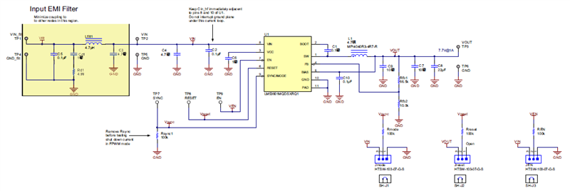
Figure 3: Schematic for EMI filtering and LM53601-Q1 power supply

There are many issues when designing automotive lighting designs, the techniques described within this blog covers the implementation of a high efficiency switching regulator to replace more traditional solutions. Using switching regulators can save space, in some case reduce overall cost and can be designed such to limit EMC. Using a device specifically designed for these types of applications can save a significant amount of time, effort and engineering cost. Get more information on TI’s products for automotive lighting applications.

Read more blogs on this topic:


How Bobby Mitra stays several moves ahead of the game

$
0
0

Bobby Mitra takes no shortcuts
Bobby Mitra – pioneer in India’s semiconductor industry, our company’s leader in the development of semiconductor solutions for industrial systems, IEEE Fellow and avid chess player – sees continual learning as an investment in the future.

“There are no shortcuts,” he said. “In every assignment I’ve ever had, I always invest – and I use that word carefully. We have to spend quality time understanding the domain, the market forces, the end-equipment markets and, most importantly, the customer requirements.”

So whether he’s broadening his personal education, accepting a new professional role, introducing a product, opening a market or learning to approach problems in unique ways, he invests time to understand deeply.

Today, Bobby leads our company’s initiatives to drive worldwide system engineering and marketing for the very diverse industrial market. This ranges from sectors such as factory automation, motor drives and building automation to grid infrastructure, medical, test and measurement, and others.

Previously, he was the president and managing director of our operations in India. His responsibilities included research and development, sales, applications, and marketing. He had one of the longest careers in the Indian semiconductor and electronics industry. He chaired the India Semiconductor Association, now called the India Electronics and Semiconductor Association, where he played a key role in shaping the Indian Electronic System Design and Manufacturing industry. He was also the president of the VLSI Society of India for many years.

Our company was the first multinational technology firm to open a research-and-development center in India, and his leadership helped create a robust semiconductor industry there. He was elected a Fellow of IEEE and the Indian National Academy of Engineering. He was also recognized as one of the top three research-and-development visionaries by the IT industry in India and named as one of the Top 10 Innovators of India.

Bobby recently was recognized in a new book, Icons of Indian IT, for his pioneering leadership and innovation in India’s semiconductor industry. He took time to answer a few questions:

How did the semiconductor industry get started in India?

“There was no semiconductor industry in India when I joined TI. We were the first multinational semiconductor company to set up a research center there. We had two big challenges. First, we had to establish our credibility within TI. We had to prove that we could deliver results from a remote location and then we had to expand our charter to become a vital research-and-development center within the company.

“But we were not an island in the technology world. So, second, we had to develop a vibrant ecosystem. The universities – which represent the future – were a big part of that. We built lasting partnerships with 700 key universities and engineering institutions in India, and we developed relationships that were beneficial to students, universities and our company.

“We also engaged other companies, suppliers and organizations to build the ecosystem from an industry point of view. Slowly, other semiconductor companies started establishing centers in India. In most cases, their first stop was TI. They wanted to learn from our experience. The India Semiconductor Association had more than 100 members from other technology companies. In many ways, these steps helped to shape the semiconductor and electronics ecosystem in India.”

How has that experience prepared you to become our company’s worldwide leader in industrial systems?

“The industrial market is very diverse. There are several hundred end-equipment applications and many large and small companies across the world that are trying to use electronics to differentiate, innovate and create what’s next. There is also increasing intelligence embedded in these end-equipment applications across factories, buildings, the grid, medical, test equipment, and other areas. The diversity of our company’s semiconductor products in analog and embedded processing is a strong fit for this market. When I was in India, multiple TI product lines invested there over time, and I realized the power of our broad portfolio.

“In the same way, it was natural to learn the many details of the industrial sector. Because I had engaged with many TI businesses in a unique capacity in India, I had an opportunity to interact with multiple companies spanning several end-equipment applications.

“When I take on a new role – whether directing our operations in India or leading the many sectors of the industrial market – I spend time understanding it. How can we win in the market? How can we position ourselves? I go deep.

“In India, we had to build the ecosystem for the semiconductor industry. From the perspective of TI technology today, we also have a systems focus that allows us to see how the integrated circuits we design and manufacture work in a system context. And we also create reference designs that show how the devices interact with each other from a product perspective.”

You earned a Ph.D after completing your bachelor of technology degree from the Indian Institute of Technology and, more recently, earned an MBA. Why is continual learning important to you?

“I come from a family of educators. I learned from them that what’s important is that the degrees teach you how to look at problems in new ways. For me, pursuing these degrees was a personal investment in new areas of learning. Blending vital on-the-job experience with diverse academic perspectives makes a strong combination.”

You’re an avid chess player. How is chess like business?

“Chess is my favorite pastime. I’ve loved the game since I was a child. It teaches you so many important lessons – driving winning strategies, anticipating competitor moves and thinking several moves ahead under uncertainty. When you add a clock to the game, it adds a dimension that is very much like the real world. You have to act fast, but still keep your focus on the strategy and direction. At the same time, you have to uncover new opportunities. And you have to learn continually.”

Converting from USB Type-A to USB Type-C™ brings greater energy efficiency

$
0
0

USB Type-C™ adoption into the personal electronic space is ramping up. Many system and product definers are asking if they should convert USB Type-A ports into USB Type-C ports, and what that entails.

There are benefits and costs to making the switch. Besides the obvious advantage of having the new USB Type-C connector, which is easier for customers to use and has a smaller form factor, the system also becomes more energy-efficient. TI has a family of products that make the conversion very straightforward.

In this post, I want to focus on USB 2.0 and USB 3.1 data systems that are 5V only. The conversion is simplest for a USB 2.0 system. Figure 1 shows a typical schematic for a USB 2.0 Type-A system. Converting this system to USB Type-C is just a matter of replacing the USB power switch, as shown in Figure 2. TI has a large portfolio of USB Power Switches for Type-A ports, so this blog is to help those using power switches such as the TPS20xxC family know how to convert to Type-C ports.

Figure 1: Traditional USB 2.0 Type-A system using a TPS2051C USB Power Switch

Figure 2: USB 2.0 Type-C system

The first thing to notice about the USB Type-C power switch is that it has more pins and more features. The configuration channel (CC) pins CC1 and CC2 perform the USB Type-C functionality. USB Type-C allows the source to change its advertisement dynamically, so TI’s TPS25821 advertises either 0.5A or 1.5A, for example, based on the state of the CHG pin.

USB Type-C hosts are required to disable VBUS when nothing is attached. This cold-socket requirement has the great advantage of allowing systems to reduce quiescent current. For example, the TPS2051C in Figure 1 must remain enabled even when there is no cable attached – and will be consuming 80µA. In contrast, the TPS25821 will not apply voltage to the OUT pin when the receptacle is empty and will consume only 1µA. The TPS25821 also indicates whether the receptacle is empty via the  pin, which the system may use to reduce quiescent current.

A USB Type-C receptacle has two pairs of USB 2.0 data contacts, but they are shorted together because the Type-C cable only has one pair of USB 2.0 data wires.

Before moving on to USB 3.1 systems, it may be a good idea for me to pause here and explain why it is not a good idea to try to implement a discrete solution. It is important that VBUS be low when the USB Type-C receptacle is empty. A USB Type-C system can connect to a USB Type-A port through an A-to-C cable. Since the USB Type-A port VBUS will always be about 5V, if the connection happens when the USB Type-C port is not cold-socket, the port with the higher VBUS voltage will drive current into the other port. Many USB Type-A port power switches do not have reverse-current protection, so they could be damaged if driven to a higher voltage.

Figure 3 shows a discrete USB Type-C implementation that implements the cold-socket requirement. It is much simpler to just use a USB Type-C power switch!

Figure 3: Discrete USB 2.0 Type-C system

In Figure 2, the  pin on the USB power switch is unused because it is a USB 2.0 system. When converting to a USB 3.1 system, however, the  pin becomes very important because the flip-ability of the USB Type-C plug requires a SuperSpeed multiplexer. You cannot use the USB 2.0 stubbing trick for USB 3.1 systems because there are eight SuperSpeed data wires in a USB Type-C cable, not just the four being used. Stubbing signals together would cause the signal to travel back through the cable again, and at the short wavelengths of USB 3.1 signals, the reflections would totally kill the signal.

There is another major change in the USB Type-C ecosystem that affects the requirements for a USB Type-A to USB Type-C conversion. Since a USB 3.1 Type-C cable may be connected in systems where VBUS reaches 20V, the VBUS wire can no longer directly power the active components in the cable (eg. a signal redriver such as TUSB544). Therefore, the electronics in the plug need a low-voltage supply from the USB Type-C host. USB Type-C hosts are required to provide this low-voltage supply onto the plug’s VCONN pin, which will be attached to either the CC1 or CC2 pin in the receptacle depending on plug orientation. The TPS25821 used in Figure 2 for USB 2.0 does not have VCONN capability, but the TPS25820 used in Figure 4 will automatically apply voltage to and discharge the VCONN pin of the cable according to USB Type-C specification requirements.

Figure 4 shows the simplest implementation for converting a USB 3.1 Type-A system (not showing the electrostatic discharge [ESD] of the SuperSpeed lines for simplicity). The TPS25820 pin controls the multiplexer so that the correct signals get routed to the USB 3.0 data system, but the addition of a multiplexer is a new burden for USB 3.1 systems.

Figure 4: USB 3.1 Type-C system

Finally, this post mainly targets USB systems that only provide the USB standard current.  However, USB Type-C provides a simple way to increase the amount of current advertised without overloading the D+/D- wires as in the CDP mode of Battery Charging (BC) 1.2. For example, you can configure the TPS25820 and TPS25821 to offer either the USB standard current or 1.5A by pulling the CHG pin high or low, while the TPS25810 can offer up to 3A.

In summary, converting from USB Type-A to USB Type-C not only allows you to keep up with the latest technology trend, but it also provides for becoming more energy efficient and easily sourcing higher power.

Additional resources


Boost your SimpleLink MCU development with the Open On-Chip Debugger

$
0
0

TI’s SimpleLink™ platform of connected MCUs continues to add capabilities to help customers optimize their development experience, recently adding Open On-Chip Debugger (OpenOCD) support for many SimpleLink devices and kits.

With built-in support for TI’s XDS110 JTAG debugging probe, the SimpleLink OpenOCD package natively supports most SimpleLink LaunchPad™ development kits and contains all required files based on the OpenOCD community mainline release.

In addition to the standard debugging and programming functions, OpenOCD offers advanced features to facilitate more automation and scripting as well as support for additional remote debugging applications.

OpenOCD enables debugging through Telnet, GNU Debugger (GDB) or with Tool Command Language (TCL) scripts using Remote Procedure Call (RPC). The Telnet and GDB interfaces are controlled through human commands and the TCL interface is controlled through machine commands (see Figure 1).

Figure 1: SimpleLink devices debugging with OpenOCD

GDB command-line debugging is one of the most popular industry tools for automating development without the need for an integrated development environment (IDE) and any associated overhead. GDB communication can be over Transmission Control Protocol/Internet Protocol (TCP/IP) or via pipes; many GDB command tutorials are available online.

With TCL scripting capability, you can develop with a high-level interface to OpenOCD and avoid writing more complex OpenOCD-specific commands. Scripts can help by addressing more complex bugs than what standard command-line tools can. TCL also offers an easy to build and use graphical user interface (GUI) for OpenOCD with minimal overhead. Telnet debugging also works with TCL commands and scripts.

OpenOCD is often combined with remote debugging environments, enabling the debugging of applications anytime and anywhere. This is very useful to support users across the globe or to debug devices that are not easy accessible. These environments are supported by the integration of three network interfaces: Telnet, GDB remote server and TCL server.

Moreover, you can use OpenOCD as a production programmer or for boundary scan testing. Programming can be accomplished through GDB or flash programming commands (see Figure 2 and Figure 3). With the help of TCL scripts, those flash commands program/verify/reset/shutdown) can easily implement the entire programming flow. With the same configuration, you can program different devices and architectures using different probes.

Figure 2: SimpleLink devices programming through Telnet (left: OpenOCD server, CLI interface; right: Telnet client)

Figure 3: SimpleLink devices programming through GDB (left: OpenOCD server, gdb server; right: GDB client)

OpenOCD enables a closer debugging experience to data flows on the device and works with a panoply of open-source tools. OpenOCD is real-time operating system (RTOS)-aware, supporting Amazon FreeRTOS and other open-source kernels to facilitate the debugging of multithreaded applications. OpenOCD easily integrates with many Eclipse-based IDEs and those supporting GDB servers, like TI Code Composer Studio™ and IAR Embedded Workbench for Arm® devices. Similarly, to program SimpleLink devices, you can use any of the supported probes within OpenOCD like TI’s XDS110, Segger’s J-Link or any probe with Arm Cortex® Microcontroller Software Interface Standard (CMSIS) debug access port (DAP) support.

You can immediately enjoy the benefits of OpenOCD and a complete open-source ecosystem. Check out the SimpleLink OpenOCD documentation for more details.

Additional resources

Get started with SimpleLink MCUs and LaunchPad development kits today:

How to charge and discharge battery test equipment

$
0
0

A battery test system (BTS) offers high voltage and current control accuracy to charge and discharge a battery. It is mainly used in manufacturing during production of the battery. Battery test equipment can also be used in R&D departments to study battery performance.

One typical application of a BTS is to charge and discharge a one-cell lithium-ion battery. Considering the voltage drop in the cable, the voltage required to do this is 0V to 5V. When the battery is charging, the power bus voltage is typically 12V in order to obtain good efficiency in voltage conversion. The bus voltage increases to 14V when the battery energy discharges back to the power bus. So the BTS requires a bidirectional converter that supports a 12V-to-14V input voltage and a 0V-to-5V output voltage. The converter operates in buck mode when charging the battery and in boost mode when discharging the battery.

The LM5170-Q1 bidirectional current controller is a good fit for this application. This device regulates the average current flowing between the high-voltage (HV) and low-voltage (LV) port in the direction designated by a DIR pin. Figure 1 is a simplified schematic of the LM5170-Q1. The two phases’ interleave topology offers up to 100A of charge or discharge current. Its integrated 5A driver helps optimize efficiency in voltage conversion, which means small power loss and good thermal performance for the system. The diode-emulation feature of the LM5170-Q1 prevents current from flowing opposite from the direction selected by the DIR pin. This feature helps protect the battery from overcharge or discharge during transient periods.

Figure 1: LM5170-Q1 simplified schematic

One critical requirement of the BTS is the current accuracy, which should be better than 0.05% of full scale. Because the LM5170-Q1 integrated current amplifier can’t meet this requirement, an external current-sensing resistor and amplifier are required to improve the current accuracy.

To demonstrate the feasibility of the LM5170-Q1 in achieving this current accuracy, TI released the 50A, 0.05% Current Accuracy Power Reference Design for Battery Test Systems to target applications that charge or discharge one-cell lithium-ion batteries with high current accuracy.

Figure 2 is a block diagram of the reference design. The lithium-ion is connected to the LV port of the LM5170EVM through a 1mΩ resistor. The HV port is connected to the 12V-14V bus. The current through the battery is sensed by the voltage drop of the 1mΩ resistor using the INA188. The output of INA188 feeds into the OP07C operational amplifier, which generates an integrating signal using the difference between the output of the INA188 and the reference voltage. The reference voltage is provided by a microcontroller not included in this reference design.

The output of the OP07C connects to the ISETA pin of the LM5170-Q1, which regulates the current flowing through the 1mΩ resistor to the current reference. The battery voltage is also sensed and regulated based on the voltage reference. When the battery voltage doesn’t reach the voltage reference, the battery current is controlled at the current reference. When the battery does reach the voltage reference, the voltage loop overrides the current loop and the battery current increases to zero.  The direction of the current to charge or discharge the battery is controlled by a logic signal (indicated as “Direction” in Figure 2). This logic signal is connected to the DIR pin of the LM5170-Q1. It also controls the INA188 input signal direction through analog multiplexers. 

Figure 2: 50A, 0.05% Current Accuracy Power Reference Design for Battery Test Systems block diagram

Figure 3 shows the current accuracy when charging the battery from 1A to 50A. The test data shows that the current accuracy is much better than 0.05%, which proves the capability of the LM5170-Q1 in a BTS application.

Figure 3: Battery Charging Current Accuracy

Table 1 shows the output voltage at different reference voltage conditions, with the voltage gap less than 0.5mV from a 0.05V-5V reference voltage, which is also good for BTS applications.

Reference voltage (V)

0.04968

0.4988

0.99788

1.99434

2.9912

3.98935

4.98531

Actual voltage (V)

0.04969

0.49882

0.99788

1.99433

2.99116

3.98935

4.98526

Table 1: Voltage Control Accuracy

The LM5170-Q1 is a good fit for applications that require an energy exchange between two power sources. Its high driver current, diode emulation and cycle-by-cycle peak-current limit features greatly improve efficiency in voltage conversion and also provide good protection during stable and transient periods. Get more information on TI’s products for battery test equipment.

Digital power control advances GaN PFC design

$
0
0
I recently shared with you the production announcement of TI’s new Piccolo™ F28004x microcontroller (MCU) series, which has been optimized for power control applications. Key features of Piccolo F28004x for high-performance power control...(read more)

In automotive lighting, it’s time to say goodbye to discrete solutions

$
0
0

Auto manufacturers are using light-emitting diodes (LEDs) beyond the traditional front, rear, day-running, stop and turn lights to make their vehicles stand out in the market. LEDs are now appearing in side markers, license plates, brand logos, welcome lights, and ambient lights.

To drive these LEDs, you must consider:

  • The accuracy of the current so that the homogeneity of the LEDs are much better.
  • The changing brightness of the LEDs, thus requiring some kind of dimming.
  • The diagnosis and protection of the LED open/short circuit, as well as thermal protection, since safety is always a key concern in automobiles.
  • How to improve energy efficiency.

LEDs have traditionally been driven by discrete solutions. Figure 1 shows three typical options: an operational amplifier (op amp) (option 1), a bipolar configuration with the power directly connected to the car battery (option 2) or some type of shunt regulation (option 3).

Figure 1: Typical discrete solutions to drive LED

Let’s take a look at option 1 first, an op amp driven from the low side. An op amp enables you to achieve relatively high accuracy (<10%) and dimmable LEDs are also possible. With this solution, however, it’s difficult to achieve the diagnostics for LED open and short circuits. And the dropout voltage is as high as 1V, which is not very energy-efficient.

Option 2 is also popular and consists of diodes and an n-channel p-channel n-channel (NPN) transistor. This solution is simple and cost-effective, but the accuracy is only about 20%, which is far from enough. The dropout voltage could be as high as 1.2V, making this solution’s efficiency even lower compared to option 1. Again, no diagnostics are available for LED open and short circuits, and no pulse-width modulation (PWM) dimming is available. This solution is really too old for today’s designs.

Option 3 is popular in applications that require very high output accuracy (<5%). The dropout voltage is extremely high (up to 3V). No diagnostics or PWM dimming are available for this solution; thus, adoption of this option is narrow and the trade-offs are huge.

Every solution has its advantages and disadvantages, but compared to discrete solutions, a low-cost monolithic solution lowers system-level component counts and significantly improves current accuracy and reliability. The TPS9261x-Q1 family shown in Figure 2 is designed just for this purpose.

Figure 2: TPS9261x-Q1 simplified circuit

The TPS92610-Q1 device is a single-channel high-side LED driver operating from an automotive car battery. It is a simple and elegant solution to deliver constant current for a single LED string with full LED diagnostics. The accuracy is as high as 7%, which is adequate for most applications.

The TPS9261x-Q1 has different package options, from small outline transistor (SOT)-23, MSOP-8 up to thermally enhanced thin shrink small-outline package (HTSSOP)-14 to support different output power levels. With this family of single-channel automotive LED drivers, you can now say goodbye to discrete solutions.


Additional Resources:

Designing tiny microphone circuits with the industry’s smallest op amp

$
0
0

Voice commands are a popular feature in many applications as a way to differentiate products in the market. Microphones are a primary component to any voice- or speech-based system and electret microphones are a common choice in applications for their small size, cost and performance.

This blog post continues our series on high-performance, cost-sensitive circuits and describes the design of a very small, cost-optimized electret condenser microphone pre-amplifier. The design uses the TLV9061, which is the industry’s smallest operational amplifier (op amp) in a 0.8mm-by-0.8mm extra small outline no-lead (X2SON) package. Figure 1 shows an electret microphone amplifier circuit configuration.

Figure 1: Noninverting electret microphone amplifier circuit

Most electret microphones are internally buffered with a junction field-effect transistor (JFET), which is biased with the 2.2kΩ pull-up resistor. Sound waves move the microphone element, causing current flow into the JFET drain inside the microphone. The JFET drain current causes a voltage drop across R2 which is AC coupled, biased to mid-supply and connected to the IN+ pin of the op amp. The op amp is configured as a bandpass-filtered noninverting amplifier circuit. With the expected input signal levels and the desired output magnitude and response, you can calculate the gain and frequency response of the circuits.

Let’s walk through an example design of this circuit for a +3.3V supply with an input of 7.93mVRMS and an output signal of 1VRMS. The 7.93mVRMS corresponds to a 0.63Pa sound-level input with a microphone and a -38dB sound pressure level (SPL) sensitivity specification. The bandwidth goals are to pass common speech frequency bandwidths of 300Hz to 3kHz.

Equation 1 shows the transfer function defining the relationship between VOUT and the AC input signal:

Equation 2 calculates the required gain based on the expected input signal level and desired output level:

Select a standard 10kΩ feedback resistor and use Equation 3 to calculate RG:

To minimize the attenuation in the desired passband from 300Hz to 3kHz, set the upper (fH) and lower (fL) cutoff frequencies outside the desired bandwidth (Equation 4):

Select CG to set the fL cutoff frequency (Equation 5):

Select CF to set the fH cutoff frequency (Equation 6):

To set the input signal cutoff frequency low enough so that low-frequency sound waves can still pass through, select CIN to achieve a 30Hz cutoff frequency (fIN) (Equation 7):

Figure 2 shows the measured transfer function for the microphone pre-amplifier circuit. The flatband gain only reaches 41.8dB or 122.5V/V, which is a little lower than the target due to the narrow bandwidth and attenuation between the high- and low-pass filters.

Figure 2: Microphone pre-amplifier transfer function

The circuit was designed with TI’s X2SON package to fit on the back side of a 6mm-diameter electret microphone. This size restriction required the use of a very small op amp: the TLV9061 has a 0.8mm-by-0.8mm footprint. Resistors and capacitors in the small 0201 size also minimize printed circuit board (PCB) area, which you could reduce further by using even smaller resistors. Figures 3 and 4 show the PCB layout.

Figure 3: Microphone pre-amplifier layout on the back side of a 6mm-diameter electret microphone

Figure 4: 3-D view of PCB design, showing a few different angles of the microphone and PCB

You can modify the design steps described above to fit different microphone sensitivities. Be mindful when designing with small amplifiers like the TLV9061 to follow the layout best practices described in this application note, “Designing and Manufacturing with TI’s X2SON Packages.”

Additional resources


There are more ways than you think to reduce conducted EMI

$
0
0

Electromagnetic interference (EMI) is a troublesome issue in certain designs, especially in automotive systems, like infotainment, body electronics, ADAS and so on. When designing the schematic and drawing the layout, designers usually minimize noise at the source by reducing the high di/dt loop area and slowing down the switching slew rate.

However, sometimes no matter how carefully they design the layout and schematic, they are still unable to reduce the conducted EMI to required levels. The noise depends not only on the circuit parasitic but is also related to the current level. In addition, the action of switch turn-on and turn-off creates discontinuous current. Discontinuous current causes voltage ripple on the input capacitor, which increases EMI.

So it’s a good idea to consider other ways to improve conducted EMI performance – adding an input filter to smooth the voltage perturbations or adding a shield to block the noise.

Figure 1 shows a simplified EMI filter, which includes a common-mode (CM) filter and a differential mode (DM) filter. Generally, the DM filter filters noise less than 30MHz and the CM filter filters noise from 30MHz to 100MHz. Both filters have an effect on the entire frequency band where EMI needs limiting.

Figure 1: A simplified EMI filter

For example, Figure 2 shows the positive and negative noise from the input wire without any filter in the infotainment system, as well as both the peak and average noise. The system tested uses TI’s SIMPLE SWITCHER® LMR14050-Q1 single channel buck converter to generate 5V at 5A and the TPS65263-Q1 triple channel buck converter to generate 1.5V at 3A, 3.3V at 2A and 1.8V at 2A. The switching frequency is 2.2MHz. The conducted EMI standard in the figure is Comité International Spécial des Perturbations Radioélectriques (CISPR) 25 Class 5.

Figure 2: Noise without any filter against the CISPR 25 Class 5 standard

Figure 3 shows the EMI result with a DM filter. The DM noise is attenuated nearly 35dBμV/m by the filter in the middle frequency band (2MHz to 30MHz). The high-frequency noise (30MHz to 100MHz) is also reduced, but still exceeds the limit level. That is because a DM filter does not effectively filter CM noise.

Figure 3: Noise with a DM filter against the CISPR 25 Class 5 standard

Figure 4 shows the noise with a DM and CM filter. Compared to Figure 3, the CM filter decreases CM noise by nearly 20dBμV/m. The EMI performance passes CISPR 25 Class 5.

Figure 4: Noise with a DM and CM filter against the CISPR 25 Class 5 standard

Figure 5 also shows the noise with a DM and CM filter (the same filter with Figure 4), but with a different layout. Compared to Figure 4, the noise in the whole frequency band increases approximately 10dBμV/m. Even worse, the high-frequency noise exceeds the standard limit.

Figure 5: Noise with a DM and CM filter against the CISPR 25 Class 5 standard

Figure 6 shows the difference in the layout that caused the different results between Figures 4 and 5. In Figure 5’s layout, shown on the right side of Figure 6, the large overlying copper (GND) and VIN trace form some parasitic capacitors. These parasitic capacitors provide a low impendence path for the high-frequency signal to bypass the filter. So in order to maximize the effectiveness of the filter, you must remove the overlying copper around the filter in every layer, like the layout shown on the left side of Figure 6.

Figure 6: Different filter layouts

Another effective way to optimize EMI performance is to add a shield. A metal shield connected to GND can block the radiated noise. Figure 7 shows the board with the suggested placement of the shield. The shield covers all components except the filters.

Figure 8 shows the EMI result with all of the filters and the shield. In Figure 8, the shield almost eliminates noise in the whole band, so the EMI performance is excellent. The shield reduces radiated noise coupling with the long input wire, which acts as an antenna. In this design, the middle-frequency noise typically couples in this way.

Figure 7: Board with a shield


Figure 8: Noise with all filters and a shield against the CISPR 25 Class 5 standard

Figure 9 also shows the noise with all filters and a modified shield. In Figure 9, the shield is a metal box enclosing the whole board; only the input wires are outside. With this shield, some radiated noise can bypass the EMI filter and couple to the power wires in the PCB, which results in worse EMI performance than the shield in Figure 8. Interestingly, the EMI result in the high-frequency band is almost the same as in Figures 4, 8 and 9 (they are all the same layout). That is because radiated noise is almost nonexistent in the high-frequency band for this design.

Figure 9: Noise with all filters and a shield against the CISPR 25 Class 5 standard

In general, adding an EMI filter and shield are both effective ways to improve EMI performance in automotive systems. At the same time, be careful with the layout of the filter and the position of the shield.  Read the application note, “Low Conducted EMI Power Solution for Automotive Digital Cockpit with LMR14050 and TPS65263” for more information.


TI partners with Hall of Fame quarterback Troy Aikman and United Way to introduce students to STEM careers

$
0
0

(Please visit the site to view this video)

More than 300 middle-school students got hands-on experience about what it could mean to pursue careers in science, technology, engineering and math (STEM) when our company teamed up with the United Way of Metropolitan Dallas and Hall of Fame quarterback Troy Aikman for the sixth annual STEM in the Schoolyard event in Dallas.

“Education is a major focus for our company and for United Way,” said Brian Crutcher, TI’s executive vice president and chief operating officer. “We had an opportunity at this event to introduce students to some pretty cool technology and show them what a STEM career could look like.”

More than 150 volunteers from TI and other Dallas-area firms guided the students from Oliver Wendell Holmes Humanities and Communications Academy through activities that included circuit design, data science and facial recognition, robotics, and coding. 

Troy, who is leading the annual fundraising campaign for the United Way of Metropolitan Dallas, kicked off the April 13 event and joined Brian and other volunteers to help the students learn about technology.

“When we consider the skills our young people will need to succeed in the future, STEM education plays an essential role that will only grow,” Troy said. “I’m proud to be part of United Way’s work to bridge the STEM skills gap for all North Texas students and empower a prepared workforce of tomorrow.”

How to achieve higher system robustness in DC drives, part 1: negative voltage

$
0
0

I recently moved to a new apartment, so I decided to go shopping for a vacuum cleaner. As I walked around the appliances section, I noticed how many of the vacuums were cordless. The manufacturers also seemed to be advertising more suction power, longer battery life and extended warranties.

One takeaway, as a customer, was that robust and reliable solutions are facilitating longer lifetimes, which in return improve a product’s reputation. This is relevant for applications like small home appliances, garden and power tools, and residential air conditioners that use electric motors. Most of these systems use DC drives such as brushed-DC (BDC) motors, three-phase brushless-DC (BLDC) motors or stepper drives. Given their high efficiency, lower audible noise and longer life spans, BLDC motors are widely used in appliances in order to achieve longer battery life, reduce cooling efforts and enable reliable operation.

Electronic motor control represents one of the main applications for MOSFET drivers. When selecting a gate driver for your DC drives, there are some design considerations to keep in mind in order to achieve higher system robustness. Part 1 of this blog series will cover negative voltage handling.

Negative voltage, in relation to a gate driver, it is the ability to withstand voltages seen at the input and output. Negative voltages result from parasitic inductances caused by switching transitions, leakage or poor layout. These unwanted voltages commonly appear in applications like motor drives, appliances and switch-mode power supplies.

Of all the issues resulting from parasitic inductances, one of the main problems for motor control is a tendency for the switch node (HS) to undershoot the ground following switching transitions. Figure 1 shows the internal parasitic inductances and board-layout inductances that exist in any design.

Figure 1 also shows that during the high-side turn-off, with continuous current flowing in the inductor, as the high-side current falls the low-side current rises. In most cases, this occurs  in the body diode for a short period of time. The current in the parasitic inductance generates a negative voltage relative to the MOSFET channel and body diode. The result is a negative voltage spike on HS, which can cause gate driver malfunction, DBOOT diode overcurrent or VHB-HS overvoltage.

Figure 1: Negative voltage on HS: di/dt effect on a gate driver

It’s important for gate drivers to have significant HS-negative voltage capabilities in order to improve robustness in your designs. For example, the UCC27710 600V driver maintains the correct output state within the voltage and time conditions shown in Figure 2. With a negative voltage capability of -11VDC across temperature, this solution offers robust operation under these conditions, which is critical for a reliable solution.

Figure 2: UCC27710 HS-negative voltage capability

Now, let’s discuss how to reduce those unwanted negative spikes. The parasitic inductances mainly come from the board layout. The layout of half-bridge power devices can be relatively tight, but what about the long trace from the FET to the bulk input capacitor?

Figure 3 shows a typical half-bridge driver and power-train layout. You can see that the MOSFETs are relatively close together, but due to PCB board size constraints, the bulk capacitor is often placed further from the FETs. This board layout path will result in source-to-capacitor parasitic inductance, which can result in large negative HS spikes.

Figure 3: Board layout path resulting in parasitic inductance

Figure 4 shows the bottom layer of the board layout. If you add high-voltage ceramic capacitors, you can place them very close to the power MOSFETs. Now the path from the low-side FET source to the capacitor is reduced significantly. Assuming that the parasitic inductance is relative to the path length, you can reduce the negative spike, as Figure 4 illustrates.

Figure 4: Improved board layout resulting in a reduced negative spike

As you can see, negative voltage handling is a critical function for gate drivers. Keep this in mind to achieve higher system robustness when designing motor-drive applications.

Additional resources

DIY with TI: Electric scooter keeps engineer on a roll

$
0
0

(Please visit the site to view this video)

At TI, we celebrate the makers and hobbyists who enjoy creating and innovating on their own time. In our ongoing DIY with TI series, we share their do-it-yourself inventions that use TI technology.

Why walk when you can scoot faster? Better yet, thought engineer Lucas Schulte while hoofing it from the train station to his office in Dallas, why buy your ride when you can build it for less?

And so began his homebuilt electric scooter project. The scooter hits a top speed of 20 mph and cost just $300 to build. Not bad for an applications engineer with no prior experience with DC motor control or lithium-ion battery cells. "I'm not the first person to make something like this," Lucas said. "But others are significantly more expensive than $300."

Born to DIY

Lucas is no stranger to DIY projects. He was born into it, even though he only discovered electronics while in high school. Growing up in rural Goliad, Texas, he and his family did their own home repairs. But, most importantly, they made things.

Once bitten by the electronics bug, Lucas went on to earn an electrical engineering degree from the University of Texas at Arlington and then joined our company. He and his colleagues build and test reference designs for our customers looking to incorporate our company’s components into their own products.

He started with a pre-built scooter frame, to which he added batteries, a motorized wheel, a microcontroller, and a motor driver booster for getting signals from the controller to the motor and other components.

Lucas Schulte A major challenge turned out to be the scooter's power supply. Lucas wanted speed and range, and for that he ended up having to build his own battery pack out of 13 lithium-ion battery cells. Connecting those cells required Lucas to design his own case out of 3-D-printed parts and short lengths of PVC pipe. "It's bolted and uses mechanical pressure to hold everything together rather than welding," he said.

Looking ahead

Lucas is already planning enhancements for his next scooter design. A new frame will allow him to hide the battery pack. He'd also like to add an active cooling system to keep the battery pack from overheating in the Texas summers. And, he said, "maybe even fantasy things like regenerative braking."

Lucas leads our TI Makerspace, a grassroots initiative that gives employees an open space to collaborate and innovate. The makerspace launched in December 2016 and has grown to about 100 members in the United States. The club offers a collaborative environment during off-hours where TIers can network, learn and work on innovative projects while surrounded by technical expertise from its members.

With the scooter complete, he’s already starting to think about his next DIY project. “Maybe an electric four-wheeler,” he said.

DIY with TI: what will you make?
To check out the products (DRV8320H and MSP430F5529LP) mentioned in this story, and more, go to ti.com/products.

Predicting failures with condition monitoring

$
0
0

Many motors and pumps are critical in factory production; a functional failure might cause a complete line stop. To avoid this, there are usually extensive preventive maintenance plans in place that require work at regular intervals. These plans are based on lifetime statistics and not on the actual condition of the equipment.

If you know the condition of the equipment, you can reduce maintenance costs as well as the risk of an unexpected breakdown. Using this knowledge to schedule repair and replacement is called predictive maintenance.

The process toward failure

You can understand the condition of equipment because there is a process leading to its final functional failure (as illustrated in Figure 1). Usually, this failure process takes time (for example, think about wear or contamination as a source of failure).

Figure 1: Failure process and cost to repair

Early indicators of failure

Fortunately, you do not have to wait until the equipment is broken – because there are early signs and signals that indicate a potential failure. The time from being able to detect a potential failure (P) until the actual functional failure (F) occurs is known as the P-F interval. Some indicators for motors with their corresponding P-F intervals that you can find in the literature include:

  • Oil analysis (months).
  • Vibration (weeks to months).
  • Power (weeks to months)
  • Thermal image (weeks).
  • Audible noise (days to weeks).
  • Heat (days).

Obviously, the earlier you can detect a potential failure, the more time you have to react, plan and execute equipment maintenance (Figure 2).

Figure 2: P-F curve – potential failure to functional failure

From regular inspections to continuous condition monitoring

Another factor you must consider is the inspection interval: How often do you check for signs of potential failure? A longer inspection interval reduces the time you have to plan and execute the repair. In the worst case (as shown in Figure 3), you might have checked the condition just shortly before observing the potential failure, so when you detect the problem at the next inspection interval, the time to schedule and execute the repair is shorter than the P-F interval minus the inspection interval.

The best method would indicate a potential failure as early as possible while keeping the inspection intervals as short as possible; in other words, observing failure indicators continuously.

Figure 3: Inspection interval

Vibration condition monitoring

Changes in vibration are very early indicators for potential failure; in addition, it is simple to measure vibration continuously. The Reference Design for Wireless Condition Monitor for Motors and Pumps Using Multi-Axis Vibration is an example for such a vibration sensor. It uses an analog three-axis accelerometer that is measured by the precision analog-to-digital converter (ADC) in the MSP432P4. The measured data is processed in the sensor node by generating a fast Fourier transformation of it. The resulting frequency-domain data determines changes in the vibration patterns but also reduces the amount of data transmitted wirelessly via Bluetooth® low energy to a gateway, smartphone or tablet.

As shown in Figure 4 on-site operators can use the data from the sensor directly for diagnostics and troubleshooting. In the cloud, you can store the data and perform further analysis on the basis of previously captured data.

Figure 4: Vibration condition monitoring setup

Conclusion

Continuously monitoring the vibration of critical assets like motors and pumps in factories provides an early indication of a potential failure and enables you to plan the maintenance of equipment based on its actual condition, thus saving money. Adding a wireless sensor that pre-processes the data is an easy and low-cost way to add this functionality to motors and pumps.

Additional resources

Shrink module size with Flip Chip On Lead (FCOL) package technology

$
0
0

Power modules are becoming increasingly popular in many market segments – the ability to buy a power supply that already includes the switching inductor is a big advantage. The main reasons engineers are choosing power modules as opposed to a discrete alternative are:

  • Reduced Solution Size. Power Modules are typically smaller than what designers can easily develop on their own. The ability to integrate active circuitry under the inductor can significantly reduce solution size and enables you to put more functions in a smaller space
  • Reduced Development Time. Power Module designers are power experts; they put tremendous effort into ensuring the components used in the module are reliable and of the right value to ensure excellent performance. They choose the optimal control topology and confirm the layout is of high quality. The result is a solution that is robust, high performance and easy to use.

In order for the power module market to continue to expand, the modules need to continue to get smaller and include more compelling features.

Power modules are built with several different manufacturing techniques, each with pros and cons. Figure 1 highlights some of the different approaches, including embedding the integrated circuit (IC) in a laminate, putting components onto a laminate and overmolding (or not), or putting components onto a metal leadframe and overmolding.

Example of various package types offered by Texas Instruments

All of these approaches can be designed with the inductor over the active circuit. In the embedded approach, the IC is integrated into the laminate and the inductor is placed on top (as in the TI TPS82130). For higher-current, laminate and leadframe-based designs (see the TPSM846C24), the active circuitry is placed under a stilted inductor. While in theory it is possible to implement these same techniques with a discrete design, in practice it is complicated to achieve in volume production.

The embedded approach enables the smallest module size for a given power level, but thermal limitations of the power IC in the laminate reduce the amount of power that this packaging technique can handle. Using a stilted inductor is also not a good approach when you need lower-current small-chip inductors.

Another factor to consider when developing a power module is how the IC is packaged. An unpackaged IC is best, as it is smaller and costs less than a packaged alternative. But it is more difficult to handle and test in production, and until now has not been a common approach. Most power modules either embed the silicon in the laminate and place the inductor over the top, or use a packaged IC mounted onto a leadframe or laminate.

In order to address the need for small size and good thermals, TI has added a new package approach to its portfolio. Called flip chip on leadframe (FCOL), a bumped die is mounted onto a leadframe along with passive components and then overmolded. TI has just released its first product with this new technology, the TPSM84209. (See Figure 2 for a look at how the module looks from the inside and outside.)

A more detailed look at the inside and outside of the TPSM84209 power module

Here are the advantages:

Smaller package size. The TPSM84209 is in a 4x4.5x2mm package. This is the smallest 28V/2.5A power module on the market. With FCOL technology – the solution is smaller than if a discrete solution was used to implement the same circuit

Overmolded package. Some engineers like to use an overmolded package. In select applications it is preferable for there to be no exposed active circuitry. Aplastic overmold also improves thermals

Improved thermals. The Θja of the TPSM84209 is just 32.7°C/W vs 46.1°C/W for the TPS82130 (a 17V/3A embedded MicroSiPTM module). This allows higher output currents at higher temperatures (see Figures 3 and 4)

Good EMI. Because the IC is mounted on a metal leadframe that is soldered directly to the printed circuit board (PCB), it is possible to design very small products that meet Comité International Spécial des Perturbations Radioélectriques (CISPR) 11 specifications. The evaluation module (EVM) for the TPSM84209 has gone through electromagnetic interference (EMI) testing at an approved Underwriters Laboratories (UL) lab and it passes CISPR11 up to Class B.

Excellent reliability. Like all of TI’s modules, the TPSM84209 has gone through an extensive manufacturing qualification process which includes tests such as high temperature storage, life test, biased humidity and board-level reliability. The package/device is specified to moisture sensitivity level (MSL) 3 and 260°C/3X reflow. 

Figure 4: TPSM84209 Efficiency vs Output Current


Figure 5: Safe Operating Area 12Vin, 5Vout

There is no single package technology that is suitable for every product or application requirement.  TI uses several different technologies to enable the optimal module performance at different power levels. The new FCOL package is a good new option for when size is a key concern. Get more information on TI’s DC/DC power module portfolio.


A new approach to system protection for industrial motor drives

$
0
0
You’re an industrial drive systems designer tasked with figuring out an approach to power protection for your system’s motor. Whatever solution you decide on must account for over-voltage, under-voltage and over-current conditions in the event...(read more)

How to select serializers and deserializers in HMI systems

$
0
0

A human-machine interface (HMI) usually includes a textual or graphical view of automated system conditions and operations. HMIs are widely used in factory automation, motion control systems, industrial robots for smarter automation, and computer numerical control (CNC) systems with highly interactive interfaces and touch-screen support. Industrial HMIs need to function within a factory setting, which requires fieldbus connectivity and low-power, fanless operation.

Thin-film transistor (TFT) liquid crystal display (LCD) modules have a variety of input interfaces such as low-voltage differential signaling (LVDS) and red-green-blue (RGB)666 or RGB888. Depending on the display interface, an HMI will require only a serializer or both a serializer and deserializer.

TFT LCD modules with an LVDS input interface only need a serializer, because the outputs of the serializer are LVDS and can directly connect to the input of the TFT LCD module. However, TFT LCD modules with an RGB input interface need both a serializer and deserializer. The deserializer converts serial LVDS data to a parallel interface in RGB format that directly connects to the TFT LCD module.

Figure 1 depicts a functional breakdown of an HMI programmable logic controller (PLC) panel. The main processor receives the video data from external memory and a wired interface, performs the digital processing, and then passes parallel RGB video data to a serializer. The serializer converts the parallel data to serial LVDS pairs and outputs the LVDS video to the TFT LCD panel. 

Figure 1: HMI PLC panel block diagram

The processor graphics unit video interface output is 18/24 bits of parallel RGB data. If there is a long cable distance between the main processor and the LCD panel (from 10m to 40m), you will need to use a high-speed serializer to serialize the parallel output data from the main processor to LVDS before it goes to the LCD video input.

When compared to other communication methods, a serializer/deserializer (SerDes) provides these advantages:

  • A robust link, with integrated emphasis/equalizer (EQ).
  • Embedded clock, data, and termination for better signal integrity (less skew, jitter, crosstalk).
  • High electromagnetic interference (EMI) resistance through differential signaling, data encoding, Spread-Spectrum Clocking SSC, and fewer parallel cables and connectors.
  • The ability to use lower-cost cables.
  • Takes up less space and makes for easy printed circuit board (PCB) layout.

How do you select a SerDes that will work well with your TFT LCD display? Some key parameters in the TFT LCD data sheet are the most imperative. The SerDes needs to meet these parameters in order to ensure that the TFT LCD display and the HMI system work properly:

  • Maximum and minimum pixel clock. The pixel clock is the product of total horizontal pixels, total vertical pixels, percent blanking, and refresh rate. For example, if there are 1,344 total horizontal pixels, 806 total vertical pixels, the refresh rate is 60Hz, and percent blanking is 29.15%, the pixel clock frequency is 1,344 x 806 x 60 x (1 + 29.15%) = 84MHz. Both the serializer and deserializer need to meet 84MHz in the pixel clock frequency range.

Equation 1 is the pixel clock formula:

Pixel Clock = H-pixels x V-pixels x Fps x (1 + Percent Blanking)                       (1)

where the frames per second (Fps) varies from 24Hz to 70Hz (60Hz is common) and the blanking varies from 3% to 39%.

  • Number of parallel RGB inputs required. 18-bit devices are designed for 6-bit RGB video for a total of 18 bits. 21-bit devices are designed for 7-bit RGB video for a total of 21 bits. 24-bit devices are designed for 8-bit RGB video for a total of 24 bits.
  • Number of serial LVDS outputs or parallel RGB outputs required. There may be three or four serial LVDS input pairs on a TFT LCD module with an LVDS interface. On a TFT LCD module with a parallel RGB interface, a deserializer is needed to convert the LVDS signals back to parallel RGB signals. The RGB signals can be 18 bits, 21 bits or 24 bits.
  • Data strobe edge. Does the display require a rising edge data strobe or a falling edge data strobe? Both the SN65LVDS93B and SN65LVDS93B-Q1 offer data strobing at rising and falling edges and are compatible with most deserializers and LCD panels.
  • Operating temperature range. SerDes devices operate in one of these temperature ranges: 0°Cto 70°C, -40°C to 85°C, -40°C to 105°C or -40°C to 125°C.

If the SerDes don’t meet these parameters, data on the TFT LCD display may display incorrectly, or not at all, and cause the HMI system to function unexpectedly.

Leave a comment below if you would like to learn more about anything discussed here, or if there is an LVDS topic you would like to see in the future.

Additional resources: 

Employee cookbook provides a taste of cultural diversity for TIers in Europe

$
0
0


When Estela Fernandez Gonzalez moved to Germany a year ago, she wanted to share her culture with new friends and colleagues. She developed a taste for cooking the traditional Spanish meals she first grew to love in her grandmother’s kitchen.

“Food means people. It’s a social activity,” said Estela, a pricing specialist for our company who enjoys cooking with friends after work.

When TIers across Europe were invited to submit recipes for an employee cookbook to raise money for the European Federation of Food Banks, she jumped at the opportunity to share her family recipe for frixuelos, a type of Spanish pancake. “This is a traditional recipe from my region, Asturias, and it’s something I wanted to learn from my grandmother. She loves cooking, and when she cooks with me she likes to be the boss. I’m the sous-chef.”

(Please visit the site to view this video)

Estela was one of more than 50 TIers who contributed recipes to the cookbook. The non-profit provided food to 6.1 million people through 37,200 European charities in 2016. To date, the cookbook has raised about 2000 Euros.

Cookbook“We are grateful to have been part of promoting the diversity of the employees of TI, and thank each one of them for their support to reduce hunger in Europe,” said Carolina Diaz-Lönborg of the European Federation of Food Banks.

A melting pot of cultures

People from more than 60 countries work for our company in Europe. In Freising, Germany, many meet regularly for lunch to speak their native languages or for cultural activities when they’re away from work. “It’s a melting pot of cultures,” Estela said.

“With this cookbook, we wanted to celebrate and raise awareness of the different cultures we have at TI while supporting those in need,” said Jean-François Fau, president of TI in the region that includes Europe, the Middle East and Africa.

(Please visit the site to view this video)

When Needhu Gunasegaran, an applications engineer, moved from his home in India to Germany to pursue a master’s degree in scientific instrumentation, cooking became a way to stay connected to his culture. He learned the basics of cooking from his mother and likes to cook for friends. In the cafeteria at our facility in Freising, he is a regular at the table where employees from India gather for lunch. He submitted a favorite recipe for chilli chicken for the cookbook.

“Having lunch with people of the same culture and background helps me reflect on where I am from,” Needhu said. “I like to keep up traditions, like celebrating Indian festivals such as Diwali and cooking traditional meals with friends.”

Smart sensors are going to change how you drive (because eventually, you won’t)

$
0
0

The dream of fully autonomous vehicles in our everyday lives is a compelling one. Imagine a world where automobiles are truly automatic: you will need only to enter a vehicle, tell it where to go and carry on with your life while you’re transported from point A to point B, without any further human interaction.

Suddenly, the national average commute of 26 minutes to the office – the longest it has ever been– begins to vanish. The anxiety and stress of driving transforms into a relaxing and productive experience.

It’s no surprise why there are so many exciting proposals and positive regulatory conversations happening around autonomous vehicles. Self-driving vehicles would fundamentally transform global transportation networks in urban areas and beyond, while also rewriting the rules around the transportation infrastructure, vehicle ownership and so much more.

The latest forecast from IHS Automotive calls for sales of nearly 21 million autonomous vehicles globally by 2035, amid pivotal developments in requisite technology such as Internet of Things (IoT) connectivity, processing power and machine vision.

Consider today’s landscape:

  • The ability of machines to connect through IoT has become a game-changer across numerous industries, but it still remains a nascent technology. Gartner Inc. predicts that there will be 20.4 billion connected things around the world by 2020.
  • Regular vision backup cameras are a common feature on vehicles today, but cameras that help beyond that are rare. Cameras that work in the visible light wavelength are insufficient for the next generation of demands because they cannot pierce or make sense of inherently chaotic environments such as rain, dust, fog and darkness.
  • Our road networks generally lack the intelligence needed to handle smart vehicles. They need to be able to understand and communicate the myriad dynamics of a busy intersection or congested highway.
  • All of these systems – from vehicle to camera to traffic network – lack robust integration. What’s needed is a complete system solution that can rapidly work together and provide a compelling, affordable, potentially safer and more efficient transportation infrastructure.

The promise of this technology is clear from a business standpoint. Research firm PwC says that by 2022, autonomous packages will have the largest incremental impact on new car sales – about $54.9 billion, up 31% annually from 2017.

Although safety packages like radar detection will generate $58.2 billion in 2022 (at an average annual growth rate of 27%), most of this value will be integrated into list prices, and eventually into autonomous packages. Meanwhile, premium vehicles are expected to contain more than $6,000 worth of electronics in five years, driving a $160 billion automotive electronics market in 2022.

Fortunately, the foundation of this future is already underway from a technology standpoint. As IoT innovation accelerates, new sensors are giving connected machines like automobiles a better way to see and interpret the world.

Perhaps most importantly, a new breed of sensors using millimeter-wave (mmWave) radar technology provides visibility at extended ranges regardless of environmental conditions. These integrated solutions use short-wavelength waves to transmit electromagnetic signals to determine the range, velocity and angle of objects in the surrounding environment. At TI, our mmWave-sensing devices integrate a 76GHz-to-81GHz mmWave radar with a microcontroller (MCU) and digital signal processor (DSP) cores on a single chip.

The benefits of these new devices are significant. Because of integration, they are smaller and consume less power at a lower cost compared to previous options. They incorporate advanced algorithms to measure the range, velocity and angle of objects for object tracking, classification or application-specific functions.

The integration of mmWave extends to advanced driver assistance system (ADAS) solutions to change how vehicles see, and how transportation systems sense the world around them. Ultimately, this integration could drive the development of safety-enhancing applications and create a safer driving environment for drivers, passengers and pedestrians.

Cruise control can now have enhanced obstacle detection. Passengers can now use gesture controls to operate convenience functions like the infotainment system. And sensors built into the seats can now monitor the health of drivers by regularly checking their heart rate and pulse.

These are among the more immediate benefits for drivers and passengers alike. Eventually, this combination of technologies will give vehicles the added powers of perception they truly need to become an automatic and everyday part of our world, enabling better-automated decisions based on a more accurate 3-D sense of a car’s surroundings.

Additional resources

The pulse of the city: Get smarter detection and tracking for intelligent transportation systems with mmWave sensors

$
0
0
Just as we leverage sensing technologies to measure individual’s breathing and heart rates , cities can actually benefit from the same technology. One of the key aspects of a smart city is a sensor-equipped intelligent transportation system that...(read more)

Being smart isn’t enough for thermostats today

$
0
0

Given how the word “smart” is bandied about when discussing IoT technology, you may wonder exactly what it means – if it has any meaning at all. If you asked me to define a smart thermostat, here’s what I’d say:

  • A device that can remember a user’s preferences is nice, but that’s what the older programmable thermostats do today. A smart thermostat should be able to learn the user’s behavior as they enter or leave the home or room.
  • It has to be able to display temperature and local weather information on its liquid crystal display (LCD) or on a smartphone or tablet.
  • The thermostat should have the ability to sense a variety of sensors like temperature, humidity, pressure, ambient light, air quality and proximity sensors.
  • It must be able to defend itself from security threats.
  • If battery operated, the smart thermostat should consume as little power as possible to allow it to run for extended periods of time without the user needing to change or recharge the batteries.
  • It must have remote configurability and control when the user isn’t home.

This may sound like a lot to ask of a single device, but it’s well within the reach of thermostat products using SimpleLink™ Wi-Fi® microcontrollers (MCUs) such as the CC3220, a dual-core wireless MCU with a dedicated Arm® Cortex® M4 application processor and a certified Wi-Fi network processor.  A diagram of the CC3220 IC can be seen below.

Figure 1: CC3220 dual core wireless MCU

Once a smart thermostat has learned a user’s occupancy patterns based on proximity detection, the next logical step is to anticipate them. That’s where features like geofencing comes in. Users can control and remotely monitor a SimpleLink MCU-connected thermostat because of its integrated Wi-Fi connectivity. In addition, the thermostat can use the location feature of the smartphone to adjust to the user’s personal comfort settings when they’re within a certain geographic distance to the home.

Since many thermostats are battery or line-powered, and geofencing requires that the thermostat to periodically interact with the internet and/or a cloud-based service, low power consumption will be essential, especially for battery-operated thermostats. SimpleLink wireless MCUs have power consumption rates that are 30% better than even previous generations. Configurable power modes include a 135mA deep-sleep mode and a 200ms secure connection from wakeup.

Another power saver is the unique SimpleLink network learning algorithm (NLA). Because the power consumption of a connected device, such as a smart thermostat, is greatly affected by the way the local Wi-Fi access point behaves, NLA learns the behavior of the access point in always-connected mode – in real time – to optimize power consumption. In addition to NLA, a SimpleLink wireless MCU supports three connectivity modes with different power-consumption profiles. The device can be “always connected,” where two AA batteries will last a year or more, “intermittently connected” with a battery life of three years and can be configured depending on the system requirements.

Save integration costs without losing reliability

The integrated networking processor core of SimpleLink wireless MCUs offloads the burden of Wi-Fi and internet communications processing from the application processor core, freeing up resources for differentiating features in the application. The network processor’s Wi-Fi connectivity is already fully certified by the Wi-Fi Alliance and that certification is transferrable, saving you from going through the often time-consuming and costly ordeal of Wi-Fi certification.

Some smart thermostats need to communicate through cloud-based services like Amazon Web Services (AWS), Apple HomeKit, Microsoft Azure, IBM Watson and others. Starter software examples and plug-ins are readily available for SimpleLink MCUs to help get to market quickly.

Additionally, the interoperability of Wi-Fi connectivity is very important for worldwide deployments. TI has been exhaustively testing this against more than 210 access points to date, ensuring reliable and robust performance when compared to other solutions.

Self defense

Connectivity raises the issue of security. SimpleLink MCUs provide protection from application storage to run-time operation, including over-the-air communications transfers. Most resources, such as intellectual property (IP) code, data, user identities, the file system and security keys are safeguarded. Both processor cores have extensive security enhancements to protect against hacking, malicious theft, hostile takeovers and other threats. Features like hardware-based cryptographic engines reduce the need for external security chips that only add cost and complexity and enable vulnerabilities when compared to a single-chip offering.

Sensible sensors

You can build a smart thermostat based on a SimpleLink wireless MCU with a variety of environmental sensors wired directly to the device or connected wirelessly as remote sensors in remote rooms. An on-chip four-channel analog-to-digital converter (ADC) can interface analog sensors to the processing cores, or one of the peripheral interfaces (such as I2C) can link to digital sensors. For example, a microphone might connect to the ADC to implement voice recognition of simple commands. Or a digital temperature sensor might use the I2C port. Air quality, humidity, pressure, ambient light, proximity or occupancy sensors can also enhance the intelligence of the thermostat while saving energy.

Listen up

There is an increasing push to further simplify the control of smart devices and smart thermostats by integrating voice activation. TI offers two different options for voice activation. One uses the CC3220 with a simple single microphone approach; the second is a more sophisticated four-microphone option that uses TI’s latest C55xx digital signal processing (DSP) integrated circuits (ICs) to enable voice activation. These options, paired with cloud connectivity offerings like Amazon Web Services (AWS), Apple HomeKit, Microsoft Azure or IBM Watson, can help solidify an even smarter thermostat.

A bright future

Based on user feedback and other research, most products are enhanced and expanded over time with additional connectivity features which can be complicated. This process is greatly simplified with SimpleLink MCUs. A cohesive SimpleLink SDK platform approach includes related technologies, like sensors and other wireless communication protocols and interfaces, along with development tools like software plug-ins, low-level drivers, code examples and hardware design kits.

If, for example, you wanted to add other wireless communication options besides Wi-Fi to the second or third generation of a smart thermostat, you could add Bluetooth® low energy as a direct interface to smartphones, or have a Sub-1 GHz radio connect wirelessly to sensors throughout the building. You might use this wireless sensor connectivity to implement a zone temperature sensing and control application. The smart thermostat could link wirelessly to an occupancy or motion sensor and a temperature sensor in a room some distance away. The motion sensor could signal the thermostat when someone enters the room so that the electronically controlled dampers on the ventilation vents could open. The room’s temperature, sensed by the temperature sensor, would adjust to match the settings stored in the smart thermostat.

This brings me back to my original question about what a smart thermostat really is. SimpleLink wireless MCUs and SimpleLink MCU platform support make it easy for you to make your thermostats as smart as you want them to be – today and in the future.

Watch this video on smart thermostats with our TI Design:

(Please visit the site to view this video)

Additional resources

Viewing all 4543 articles
Browse latest View live


<script src="https://jsc.adskeeper.com/r/s/rssing.com.1596347.js" async> </script>