Quantcast
Channel: TI E2E support forums
Viewing all 4543 articles
Browse latest View live

Is charge injection causing output voltage errors in your industrial control system?

$
0
0

Designers working on fast-switching data-acquisition systems often complain about random spikes, fluctuations, excessive noise or other kinds of unexpected voltage on their analog input channels. The common reason for these problems is impedance mismatching. When driving multiplexed systems with a high source impedance compared to the input impedance of the control system, you may see voltages from one scanned channel reflected on another scanned channel.

What if the source impedance and input impedance match but the unexpected voltage still persists?

Whether it is an industrial control system or any fast-switching data-acquisition system, more than one factor can cause an output voltage error when switching channels. However, for the purposes of this blog we’ll focus on one cause in particular, charge injection from the multiplexer. It is called charge injection because the charge within the device gets redistributed and can be pushed to the output when the device turns on and off.

In an industrial control system, a multiplexer toggling from one channel to the next can introduce a small charge on each channel. The lack of a path in the open channel for this charge to dissipate affects the voltage of the channel, which leads to an output voltage error. You might see an incorrect reading when scanning the analog input channels at a high rate.

Let’s explore two scenarios for a better understanding of charge injection and how it impacts the output voltage in a multiplexed system.

In the first scenario, a large load capacitance (CL) limits the bandwidth of the system. When the select pin (SEL) of the multiplexer toggles from low to high (or off to on, as shown in Figure 1), the gate of the MOSFET is subjected to a step voltage. This step voltage injects charge into the output of the switch through the parasitic gate-to-drain capacitance (CGD). The change in output voltage depends on the amount of charge injected (QC) and the load capacitance (CL).

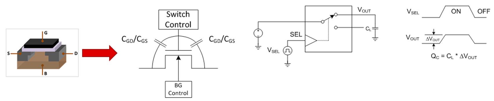
Figure 1: Switch capacitance structure


Based on Equation 1, you can see that a large CL will minimize the effect of charge injection at the output of the multiplexer:

(∆VOUT = Qc / CL)                    (1)

This will limit the bandwidth of the input signal, however, as the multiplexer’s 3-dB cutoff frequency depends inversely on CL.

In the second scenario,we see what happens when sampling the switch output after the signal stabilizes before switching to the next channel. Unfortunately, this is not an option in industrial control systems that require a fast sampling frequency, so the best option is to choose a multiplexer with very low charge injection.

As shown in Figure 2, you can minimize the effect of charge injection if the internal parasitic capacitance that injects the error (CDG) is small. Typically, multiplexers with a lower on-capacitance have a lower charge injection.

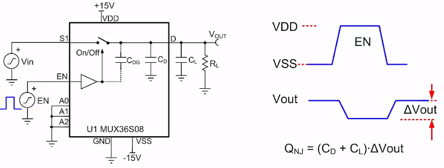
Figure 2: TMUX6104 charge injection test setup

For better accuracy, not only should the charge injection be low, but it should also remain flat across the system’s input voltage range.

Since charge injection is a multiplexer parameter that varies with supply voltage, different source voltages may produce a nonlinear shift in output voltage readings - causing operational errors. In order to make the system more robust, a design engineer should pick a multiplexer that not only has very low charge injection but also remains flat across the application’s input voltage range.

The TMUX6104 precision analog multiplexer uses special charge-injection cancellation circuitry that reduces the source-to-drain charge injection to as low as -0.35 pC at VSS = 0 V, and -0.41 pC in the full signal range.

Figure 3 is a charge-injection graph of the TMUX6104 across a supply voltage range of ±15 V. As you can see, when compared to a competing device, not only is the charge injection low but the variation of charge-injection performance across the input voltage range is minimal, making it a good fit for fast-switching industrial control systems.

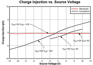
Figure 3: TMUX6104 charge injection vs source voltage

Conclusion

Charge injection is a measurement of unwanted charge due to the redistribution voltage when a switch goes from on to the off state. It shows up as a voltage change introduced at the output of the switch when the channels are switched. For this reason, it is recommended that design engineers select a multiplexer with very low charge injection for a fast-switching data acquisition system.

Additional resources


Automotive audio from the inside out: more channels, more power, more applications than ever before

$
0
0

Photo credit: MJC Classic Cars

When I was a teenager, I was lucky enough to own my dream car – a gleaming 1977 Camaro Type LT. I bought it used with about 50,000 miles already on it, and everything about it was perfect, except the factory radio. So like many proud car owners at the time, I upgraded to the latest technology: a sound system with a cassette player, very large and impressive-looking, a two-channel power amplifier with 30 W per channel into 4-Ω speakers (120-W peak power!) and two 6-inch-by-9-inch oval speakers for the rear window deck. I was ready to roll, and the sound of ZZ Tops “I’m bad, I’m nationwide” announced my arrival everywhere I went.

This was a huge improvement over the factory-installed sound system, and I had the car throughout college and even during my first few years at TI, when a dark car with a black interior and no air conditioner became completely impractical during hot Texas summers.

Today, teenagers and other purveyors of loud music and good sound quality don’t have the same struggles; the factory-installed sound systems of modern vehicles satisfy most drivers.

Car audio is more than speakers

At TI, we make circuits and components that span the entire audio chain between the signal’s source and the speakers. Our audio components make everything work, from the cluster chime audio, to the entertainment system that plays your music, to the systems that handle automatic emergency phone calling and active noise cancellation.

These components – processors, class-D amplifiers, data converters and power management – are the building blocks for every audio system in a typical passenger vehicle. From this unique vantage point, we can see the bigger industry trends moving automakers and their suppliers. 

For one, better-quality systems have made their way into less-expensive vehicles while pricier cars are getting outfitted with more channels that connect an increasing number of speakers. The result is better sound fidelity and richness, as well as audio systems with more capabilities. 

What this means for car owners is that they’re getting a better sound experience from their infotainment systems. Many vehicles are now equipped with small, lightweight and powerful external amplifiers, subwoofers and speakers throughout the cabin. These can boast up to a kilowatt of audio power with theatrical 360-degree surround-sound reproduction. 

Engineers can also design-in microphones throughout the cabin for noise cancellation, which neutralizes road and environmental noise for a quieter ride. 

Audio systems are even included in advanced safety features, like an automated eCall system that connects drivers to an emergency dispatcher through an automatic or manual trigger, and collision-avoidance and lane-departure warnings.

From Europe to Asia and farther afield, every manufacturer is increasing the audio technology in their vehicles, and drivers are raising their expectations accordingly. That’s good news for those who like the new safety, infotainment and connectivity features.

Preparing for an electric, autonomous future

Broader automotive developments are also pushing the evolution of audio systems. That’s why we’re already marketing components to help carmakers and suppliers build the future.

One important audio application that no one ever needed to think about before has to do with electric and hybrid vehicles. Because these machines aren’t powered by loud combustion engines, they run on virtually silent electric motors. In some areas, regulations now exist that require electric vehicles to audibly alert nearby pedestrians of their presence at low speeds. Consequently, engineers are developing virtual engine sound systems with speakers outside of the cabin.

That situation is just one new puzzle that carmakers have asked automotive audio engineers to solve in a rapidly changing industry. The next big challenge will come when autonomous passenger vehicles start rolling off the production line. These self-driving machines represent a new horizon for audio and infotainment because they’ll be entertainment delivery devices as much as they’ll be transportation. 

Just imagine: You could participate in a video conference for work while you’re on your way to the office or watch a movie with full theatrical sound while on an extended road trip. The audio system will support all of that and more. 

Many of the devices for this future already exist, though, and with all of the power that these systems will demand, we’ll very likely move away from the typical 12-V electrical systems in vehicles now to a new standard of 48 V. At that voltage, we can operate more systems with higher efficiency.

It’s an exciting time to be in the automotive audio space because we’re helping automakers and suppliers as they go back to the drawing board to completely rethink their offerings. The result is going to be sound and communication capabilities that this industry has never seen before.

Additional resources

Achieving the programmable power supply function in USB PD applications

$
0
0
As smartphones continue to get smarter and larger, battery capacitance is also increasing. Being able to quickly charge a battery is a crucial aspect to consider in power delivery. The rise in popularity of USB Type-C™ with USB Power Delivery (PD...(read more)

Half the space, double the power: How gallium nitride is revolutionizing robotics, renewable energy, telecom and more

$
0
0

From brick-like cell phones to heavyweight television sets, power supplies have a history of taking up an unsightly amount of space in electronics – and the need for higher power density has only continued to soar.

Innovation in silicon power supplies helped cut these old models down to a more manageable size, but those improvements have been mined to the limit. Silicon simply can't run at the frequencies necessary to deliver more power without growing in size. That's a critical factor for 5G wireless network rollout, for the future of robotics and for technology from renewable energy to data centers.

"Engineers have reached the limit – they can't push more power in the space they have and they don't want to increase the space their equipment needs," said Masoud Beheshti, a product manager at our company. "If the form factor can't change, the only knob you can play with is power density."


 Learn how you can achieve higher power density with our portfolio of GaN devices.

GaN's prime-time moment

For more than 60 years, silicon has been the basis of the electrical components that convert alternating current (AC) to direct current (DC) and change DC voltage to fit the needs of everything from mobile phones to industrial robots. And while the necessary components have been refined and optimized, physics has caught up with silicon.

But a new breed of power supply and conversion systems based on gallium-nitride (GaN) is solving the problem, generating less power waste and also less heat – which is critical since higher temperatures can increase operating costs, interfere with networking signals and lead to premature equipment failure.

GaN can process power at higher frequencies and with greater efficiency – it can deliver power with half the loss of a silicon component in as little as half the space. That improves power density, a critical concern for customers who need more power without giving up more space in their designs.

Higher frequency switching means that GaN can also convert wider ranges of power in a single step, reducing the need for additional power converters in complex devices. Because each power conversion introduces more waste, this advantage is critical for a growing number of high-voltage applications.

A 60-year technology doesn't disappear overnight, but after years of research, real-world trials and reliability testing, GaN is more than ready to become the future of power density. Our company has put GaN devices through 20 million hours of accelerated reliability testing at higher temperatures and voltages than silicon. In that much time the GlobalFlyer jet – the world record holder for long-range flight – could make 259,740 trips around the globe.

"We made sure the GaN process, technology and devices are fully qualified and ready for mass production," Masoud said.

Our company is sharing these GaN qualification protocols with the Joint Electron Device Engineering Council standards body, and will steer its GaN qualification committee.

Where GaN will go next

GaN is already replacing silicon in key industries where improved power density is a premium feature. "Now that our company has mastered our GaN packaging and testing, customers have a new and reliable power converter option anywhere power density is a priority," said Arianna Rajabi, a product marketing engineer at our company.

These industries are among the best candidates for mainstream, mass-produced GaN power supplies:

Manufacturing:Today's typical robot arms don't actually contain all of the electronics needed to make the arm work. Power conversion and motor drive components are so large and inefficient that they are often located in separate cabinets, cabled over long distances to the arm itself. This reduces the productivity per cubic meter of industrial robots. GaN will make it easier to incorporate drive and power conversion inside the actual robot. That will streamline designs, reduce inefficient cabling and lower operating costs.

Data centers: Spurred by the insatiable demand for more digital services, the data center industry is in the middle of an overhaul to run directly from 48-volt DC power. Traditional silicon power conversion cannot efficiently go from 48 volts down to the low voltages required for most computing hardware in a single step. Creating intermediate steps reduces data-center power efficiency. GaN can step down from 48 volts to point-of-load before being delivered to servers and chips. This can reduce power distribution losses significantly and cuts conversion losses by 30 percent.

Wireless services:The move to blanket populations with comprehensive 5G cellular networks requires network operators to deploy higher-frequency equipment running on more power. Network operators don't want to increase the size of cell tower equipment, so GaN's power-density advantages will play a significant role.

Renewable energy: Renewable energy generation and storage also requires power conversion steps, so GaN's efficiency advantages are key. Since renewable energy plans often use a smart grid approach that stores energy for later use – when wind turbines are still or solar panels aren't being powered by the sun – being able to switch power in and out of large-scale batteries more efficiently is a great benefit. Our company and partners have demonstrated GaN's ability to convert 10 kilowatts of renewable energy generation with 99 percent efficiency, a key benchmark for power utilities.

Over time, GaN will continue to expand into applications like consumer electronics, allowing for thinner flat-panel displays and reduced waste in rechargeable devices.

"If you just need a 3 percent or 4 percent efficiency improvement, you can get that other ways," Masoud said. "But if you need to double power density, GaN is your only option."

Which multichannel buck converter layout offers better EMI performance?

$
0
0

Designers often use several DC/DC buck converters in automotive systems to support the multiple power rails. There are several considerations when selecting these types of buck converters, however. For example, you need to select high-switching-frequency DC/DC converters (operating above 2MHz) for automotive infotainment/head units to avoid interference with the radio AM band, and you also need to reduce solution size by selecting relatively smaller inductors. In addition, high-switching-frequency DC/DC buck converters can also help reduce the input current ripple to optimize the size of input electromagnetic interference (EMI) filters.


However, compliance with required EMI standards is critically important for major automotive original design manufacturers (ODMs) who are trying to build the newest systems for cars. The requirements are very stringent, and manufacturers must comply with standards like Comité International Spécial des Perturbations Radioélectriques (CISPR) 25. In many cases, if the manufacturer doesn’t meet the standard, automakers cannot accept the design.


Thus, choosing a layout for a DC/DC buck converter is key. Optimizing the power loop through which high current flows through is very critical to achieve good EMI performance.


Taking the LMR14030-Q1 DC/DC buck converter as an example, Figures 1 and 2 show two different printed circuit board (PCB) layouts for a dual-channel buck converter. The red line shows how the power loop flows in layout. The flow direction of the power loop in Figure 1 is a U type and in Figure 2 is an I type. These two kinds of layouts are the most common in automotive and industrial application systems. So which one is better?


Figure 1: A U-type layout


Figure 2: An I-type layout


Conducted EMI is sub-divided into differential-mode and common-mode categories as the two modes are similarly measured but controlled through different methods. Differential-mode noise is derived from the rate of current change (di/dt), while common-mode noise is generated from the rate of voltage change (dv/dt). The critical point for EMI performance is how to make the parasitic inductance as small as possible.


Figure 3 is an equivalent circuit for a buck regulator. Most designers know how to make Lp1, Lp3, Lp4 and Lp5 as small as possible but ignore Lp2 and Lp6. A U-type layout has a smaller parasitic inductance on Lp2 and Lp6 compared to an I-type layout. In a U-type layout, when the high-side metal-oxide semiconductor field-effect transistor (MOSFET) turns on, a shorter power loop will contribute to better EMI performance.


Figure 3: Buck regulator equivalent circuit


In order to verify what the best layout is, measuring the EMI data is essential. Figures 4 and 5 compare the conducted EMI. As you can see, the EMI performance for the U-type layout is better than the EMI performance for the I-type layout, especially at high frequencies.


Figure 4: U-type EMI performance in phase-shift mode


Figure 5: I-type EMI performance in phase-shift mode


Adding a filter is an effective way to improve EMI performance. Figure 6 shows a simplified EMI filter, which includes a common-mode (CM) filter and a differential mode (DM) filter. Generally, the DM filters noise less than 30MHz and the CM filters noise from 30MHz to 100MHz. Both filters have an effect on the entire frequency band where EMI needs limiting. Figures 7 and 8 compare the conducted EMI with both a common-mode filter and a differential-mode filter. The U-type layout can pass CISPR 25 Class 3 standards, but the I-type layout cannot.


Figure 6: A simplified EMI filter


Figure 7: U-type EMI performance using a DM and CM filter


Figure 8: I-type EMI performance using a DM and CM filter


As you can see, a U-type layout achieves better EMI performance than an I-type layout. See the application report “How SYNC Logic Affects EMI Performance for Dual-Channel Buck Converters” for more information.

Designing a magnetically immune polyphase smart meter, part 3: comparing isolated shunt sensing architectures

$
0
0
In part 1 of this three-part series, I discussed the isolated shunt sensing building blocks , and in part 2, I presented an overview of two different shunt sensing architectures . In this installment, I will compare the two architectures. Table 1 summarizes...(read more)

3 ways augmented and virtual reality are transforming the factory floor

$
0
0


Reality technologies aren’t just for video games. Whether it's a machine operator using goggles for directions or an engineer seeing a plant before construction starts, manufacturers are eagerly adopting virtual tools to streamline how they create, craft and complete their production line.

Augmented reality (AR) and virtual reality (VR) head-mount displays are making important headway into how factories are run and even designed, saving time and money. More than one in three manufacturers have already adopted the twin technologies or plan to in the next three years.1


 Learn how our integrated circuits and reference designs can help you create lightweight, reliable augmented/virtual reality headsets.

"I definitely see AR and VR technologies being applied more and more in manufacturing,” said Miro Adzan, a general manager at our company. “They can increase efficiency, cut costs and reduce injuries."

Here are three areas where AR and VR technologies can make a difference on the factory floor:

Futuristic instruction manuals

Factory workers assemble hundreds or thousands of components in a particular order as fast as possible. Imagine if they could wear glasses that give a quick, graphical hint about where to put a hand to pick the right component. Smart headsets and glasses– which blend virtual imagery, instrumentation and words into what people are really seeing – can put digital instructions about how to build a product or run a specific machine directly within an operator’s field of view, keeping hands free to handle machines on task rather than browsing through hundreds of printed pages.

“This supports the production process and reduces training time, allowing you to quickly move from one product to another,” Miro said. “You can also help prevent workers from doing something the wrong way by guiding them through the correct process.”

Better-maintained machinery

While walking the manufacturing line, engineers can easily see the status of each individual machine – including how long it’s been running, its current output and its number of failures. Image quality, brightness efficiency and high contrast, which are highlights of our company's DLP® Pico™ display products, create rich AR displays that help virtual information naturally blend into the real world.

By simply scanning the machine’s barcode, its server can upload status information or send maintenance instructions straight to the engineer’s glasses. If there’s a jam, for example, AR can give insight into how a machine’s subsystems work together and help workers visualize whether parts can be reached and repaired without dismantling the entire unit.

"You can dynamically change what you're looking for with the click of your fingers," Miro said.

Virtual build-outs

Factory workers aren't the only ones benefiting from virtual technologies during the manufacturing process. Engineers are adopting VR to see how factories may look before construction ever starts, said Jesse Richuso, a product marketing engineer at our company. They can create optimum arrangements for machinery, improving worker efficiency and lowering cost before the foundation is even laid.

“Advancements in depth sensors built in to headsets combined with light field or multi-focal plane displays, which help the brain think that a virtual object is located at the correct distance from the viewer, could improve virtual renderings so that designers, architects and manufacturers can more effectively engage with computer-generated 3D modeling,” Jesse said.

While AR and VR tools are already at play in factories, such technologies are quickly expanding – and in some cases becoming standard tools – building a more seamless experience for manufacturers from the foundation up.

“They’re touching everything you can imagine on the factory floor,” Miro said.

1According to research firm PwC

Industry 4.0 spelled backward makes no sense – and neither does the fact that you haven’t heard of TI’s newest processor yet

$
0
0
The new, highly integrated Sitara™ AM6x processor family provides industrial-grade reliability and features quad and dual Arm® Cortex®-A53 core variants that are built to meet the rapidly evolving needs of Industry 4.0 applications in factory...(read more)

How to reduce distortion in high-voltage, high-frequency signal generation for AWGs

$
0
0

With technology emerging on a daily basis, there’s an ever-growing demand to generate faster high-voltage signals, and the requirement is often driven by the end equipment. These end equipments can be anything from increasing the speed of an arbitrary waveform generator (AWG) and high-voltage clock generators to driving the input of power field-effect transistors or semiconductor test equipment.

The increased speed requirements from high voltage and current put immense pressure on the last-stage output driver amplifier to not distort the high-frequency sinusoidal signal while still being within the thermal limits of operation. High-voltage, high-frequency signal generation becomes even more challenging for an output amplifier when a low-resistive or high-capacitive load drive is involved; the amplifier can become limited in its maximum linear output current drive when you need a high voltage swing at a high frequency. Slew-rate limitations cause an increasingly distorted output signal, and the amplifier cannot source or sink the required output current at high frequencies.

In this post, I’ll focus on improving the distortion performance of a high-voltage, high-frequency sinusoidal signal while driving a low-resistive or high-capacitive load.

To understand the slew-rate limitation, I slightly modified the slew-rate equation for large-signal bandwidth in terms of peak output current (IP), as shown in Equation 1:

where f3dB is the -3-dB bandwidth of the amplifier for a given peak output voltage (VP) and RLOAD is the total resistive load at the amplifier’s output.

To maintain a constant slew rate, IP should increase for a given VP with RLOAD. Depending on RLOAD, this linear output current requirement could be quite significant, which automatically places severe constraints on the amplifier’s output current drive capability while limiting high-frequency operation. For capacitive loads, the effect of reduced linear output current is even more pronounced because of reducing impedance with increased frequency.

An effective way to counter this output current drive limitation is to use load sharing to boost the drive. The concept of load sharing is to have multiple parallel amplifiers drive a shared output load, where each amplifier is driven by the same input source (VIN), as shown in Figure 1. Driving a shared output load with multiple parallel amplifiers effectively reduces the output current requirement of each amplifier by 1/N, where N is the number of parallel amplifiers. Each parallel amplifier’s output is at the same voltage because they are driven from the same VIN.

 Figure 1: N Parallel THS3491 amplifiers in a load-sharing configuration

Figure 1: N parallel THS3491 amplifiers in a load-sharing configuration

Assuming that the feedback (RF), gain (RG) and output series resistor (RS1) are perfectly matched, Equation 2 gives the input-to-output transfer function at the individual amplifier’s output VO(i):

Equation 2

where i = 1 to N amplifiers in a load-sharing configuration.

Equation 3 expresses the input-to-output transfer function at VOUT of the resistive load (RL1):

Equation 3

where  which is the combined output load of N amplifiers in a load-sharing configuration.

Equation 4 calculates the individual amplifier output current drive for N amplifiers in a load-sharing configuration:

Equation 4

Let’s take an example of a single THS3491 amplifier driving an RLOAD of 20 Ω at 20 VPP. The required output current drive in this scenario is ±500 mA. Operating from ±7 V to ±15 V, the THS3491 offers 900-MHz bandwidth while achieving a 20-VPP output voltage swing at 100 MHz and driving an RLOAD of 100 Ω. Even though the THS3491 can support a peak output current of ±500 mA, its output can look distorted (or triangular) on a scope because slew-rate limitations prevent the ability to source/sink the required output current at high frequencies. (This reduction in output current across frequency is true for any high-output-current operational amplifier [op amp].) Using two THS3491 amplifiers in a load-sharing configuration splits the output current drive equally between the two amplifiers at ±250 mA, resulting in a less distorted output waveform across frequency.

Figures 2 and 3 show second (HD2) and third harmonic (HD3) measurements, respectively, comparing two, three and four THS3491 parallel amplifiers while driving 20 VPP with an RLOAD of 20 Ω. Table 1 lists the respective series and shunt resistor values used to create an RLOAD of 20 Ω. As you can see from the distortion plots, there is clearly an advantage of improved distortion performance in the load-sharing configuration. The harmonic distortion degrades beyond -30 dBc at 60 MHz with two parallel amplifiers. However, with three or four parallel amplifiers, the output current drive strength extends well beyond 100 MHz for the same 20-VPP output swing.

Figure 2: HD2 vs. frequency for parallel THS3491 amplifiers; test conditions

Figure 2: HD2 vs. frequency for parallel THS3491 amplifiers; test conditions: VO = 20 VPP, RLOAD = 20 Ω

Figure 3: HD3 vs. frequency for parallel THS3491 amplifiers

Figure 3: HD3 vs. frequency for parallel THS3491 amplifiers; test conditions: VO = 20 VPP, RLOAD = 20 Ω


 Table 1: Output resistor values for a THS3491 parallel amplifier configuration to create an RLOAD = 20 Ω

You can deduce two things from this load-sharing approach:

  • Each additional amplifier now has to output less current for the same output voltage swing, extending the frequency of operation beyond the f3dB point.
  • An increase in the number of parallel amplifiers enables the circuit to drive a heavier output load for the same output swing and operating frequency. This is because of the increased output current boost offered by parallel amplifiers.

One thing to note is that the use of load-sharing configuration has the disadvantage of reduced stability because of the increased capacitive load caused by long input and output printed circuit board (PCB) signals. Output push/pull current mismatching with increased system power dissipation is another byproduct of this approach. All of these factors will eventually determine the maximum number of parallel amplifiers that you can add.

Additional resources

Our isolators are certified. Are yours?

$
0
0

We use electrical gadgets every day, and there are applicable, high-voltage safety standards for designers to follow to help confirm that the gadgets that they design operate as expected from a safety perspective. Texas Instruments Inc. (TI) takes great care to produce components that meet component-level safety requirements of these standards.

Today, electrical equipment manufacturers use digital isolators for a variety of reasons, including safety and data integrity. If functional (non-safety) insulation is necessary, then the manufacturer’s main concern is proper functioning of the equipment.  On the other hand, if protecting against potential electric shock hazard is a requirement, many end equipment OEMs use third party, independent regulatory compliance certification approvals including consideration for basic, double or reinforced insulation. Today, many end equipment designers frequently use digital isolators or semiconductor components with integrated isolation to provide the required level of insulation.

Basic insulation helps to provide a minimum level of protection against electric shock. For safety purposes, a supplementary insulation in addition to basic insulation may be required. Insulation comprising both basic and supplementary insulation is called double insulation. Reinforced insulation is a single insulation system which provides a degree of protection against electric shock equivalent to double insulation. Reinforced insulation may comprise several layers that cannot be tested individually as basic insulation or supplementary insulation. Test & Measurement (T&M) equipment and Adjustable Speed Motor Drives are examples of end equipments that may require reinforced insulation.

TI’s isolation integrated circuits (ICs) are tested and certified for electrical insulation strength by multiple independent certification laboratories around the world. A typical TI isolation product might have electrical safety approvals bearing investigation and certification from the following five agencies:

  • Underwriters Laboratories (UL)
  • Canadian Standards Association (CSA)
  • Association for Electrical, Electronic and Information Technologies (VDE)
  • Technical Inspection Association (TUV)
  • China Quality Certification Center (CQC)

UL is headquartered in the United States, while CSA is a Canadian organization. VDE and TUV are based in Europe and CQC is a Chinese agency. UL, CSA, VDE and TUV all are international entities with worldwide presence. 

Once an isolation product manufacturer like TI obtains electrical safety certifications from each of the desired independent test agencies, equipment manufacturers can confidently use the devices in their products worldwide, provided the certified device’s ratings and other conditions of acceptance are effectively covered in the end product. Certification agencies not only test and evaluate digital isolators during qualification, but they also perform frequent audits of production facilities to help confirm that isolator manufacturers maintain the minimum electrical functional safety standard performance as initially qualified by the certification agencies.  By using certified digital isolators, OEM end equipment manufacturers greatly benefit in terms of cost and time by avoiding extensive high-voltage insulation testing of the TI Isolator during the end-equipment certification by these agencies.

TI’s isolation ICs are third-party certified for multiple component and end-equipment electrical safety standards. Component standards such as German Institute for Standardization (DIN) VDE V 0884-11 (VDE V 0884-11):2017-01 and UL 1577 evaluate the intrinsic insulation characteristics and high-voltage capabilities of TI isolators. End-equipment electrical safety standards such as International Electrotechnical Commission (IEC) 60950-1, IEC 61010-1, IEC 60601-1 and Guobiao (GB) 4943.1-2011 stress the insulation capabilities of isolators in the context of specific end-equipment requirements. Table 1 shows various electrical safety certification standards providing the safety requirements for digital isolators.

Electrical safety standard

Description

DIN VDE V 0884-11 (VDE V 0884-11):2017-01

Magnetic and capacitive coupler for basic and reinforced isolation

UL 1577

Standard for safety: Optical isolators

IEC 60950-1

Information technology equipment – Safety – Part 1: General requirements

IEC 61010-1

Safety requirements for electrical equipment for measurement, control and laboratory use – Part 1: General requirements

IEC 60601-1

Medical electrical equipment – Part 1: General requirements for basic safety and essential performance

GB 4943.1-2011

Information technology equipment – Safety – Part 1: General Requirements

Table 1: Component and end-equipment electrical safety standards

Reinforced certified digital isolators

To be VDE-certified as a reinforced insulator at the component level, digital isolators have to pass a minimum surge isolation test voltage of 10,000 VPK. Some of TI’s reinforced isolators are able to meet up to 12,800 VPK surge level and thus clearly pass the minimum criteria set by the VDE standard.

Check out the ISO7842, one of the industry’s highest rated working voltage digital isolators made today, or visit our isolation page to find the best digital isolator for your design.

Additional resources

Delivering a smooth transition from AC to PoE power

$
0
0

As the number of interconnected devices in the electronics market continues to grow, it becomes increasingly important to ensure interconnectivity between data-sensitive end equipment like wireless access points (WAPs), Internet Protocol (IP) cameras and security systems. Otherwise, data loss could occur, resulting in the loss of valuable information such as surveillance data. For data-sensitive applications like these, TI is here to help guide you on how to minimize the risk of data loss for Power over Ethernet (PoE) applications.

One method of decreasing the probability of data loss in a PoE system is to implement hitless failover, which enables the transition from main power to backup power without a loss of power at the load (in other words, the load does not reboot/restart and continues in normal operation). Hitless failover helps ensure continuity of service, lowering the probability of power loss and data outages.

Let’s walk through an example to see how you can implement hitless failover with the Dual-Input Redundant PoE PD with Smooth Transition Reference Design and a WAP like the one shown in Figure 1 with dual PoE inputs and a single AC/DC wall adapter input.

Figure 1: WAP with dual PoE and single AC/DC adapter inputs

In this example, the goal is to avoid data loss at all costs. Implementing three power supplies (two DC/DC PoE supplies and one AC/DC wall adapter supply) decreases the probability of power (and thus data) loss. In the event that the primary power source is unavailable due to harsh conditions, accidental trips or cable damage, one of the secondary power sources quickly transitions to become the main power source without dropping the output voltage at the load.

To implement hitless failover, you will need to choose a PoE PD device that has the automatic maintain power signature (MPS) and inrush delay features integrated – devices like TI’s TPS2372 or TPS2373 Institute of Electrical and Electronics Engineers (IEEE) 802.3bt PoE PDs, which can power loads up to 71W. The auto MPS feature is an electrical signature presented by the PD to assure the PSE that it is still present after applying the operating voltage. This automatically generated signature allows the PD to remain connected to the power sourcing equipment (PSE) and in active standby mode in the event that the main power supply goes down.

Now, let’s take a look at the hitless failover power transition as shown on the oscilloscope. In the reference design the adapter has power-supply priority over PoE1 and PoE2. Now, imagine that the adapter supply fails.

As shown in Figure 2, the output voltage of the AC/DC adapter (green) suddenly drops to zero while the output voltage of the secondary power source PoE2 (blue) transitions to being the main power source. During this transition, the input voltage to the WAP (yellow) remains constant at 5V. This enables the load to remain powered and for data to transmit continuously, even during the transition between power supplies.

Figure 2: Adapter and PoE power transition with hitless failover

Hitless failover power transition has become increasingly important due to the need for data-sensitive end equipment to avoid the loss of data transmission. If you are interested in enabling hitless failover in your PoE PD design, consider using a device with auto MPS and in-rush delay integrated such as TI’s TPS2372 or TPS2373 and the reference design I described here.

Additional resources

How to speed SSD program time with a boost converter

$
0
0

Solid-state drive (SSD) storage is becoming more popular in PC, data-center and telecom applications, offering the benefits of faster speeds and a more compact size compared to Hard Disk Drive (HDDs). The new Peripheral Component Interconnect Express (PCIe) Non-Volatile Memory Express (NVMe) Host Controller Interface Specification SSD offers three times faster write speeds and six times faster read speeds compared to traditional Serial Advanced Technology Attachment (SATA) SSDs.


However, increasing Not-AND (NAND) flash write and erase speeds, as well as solving the thermal dissipation, impose big challenges on SSD designs.


A power supply is required to support the write/erase of the NAND chip, as shown in Figure 1.


Figure 1: Write/erase the NAND flash cell


Equation 1 calculates the current during write/erase as:


I = C * (dVs / dt) + (Vs / R)                             (1)


For instance, if C is around 100 pF, R is around 1 MΩ. If write/erase completes in 100 ns, the current is around 12 mA. For an application like enterprise storage, a larger capacitance (increasing C) and faster speeds (decreasing t) require a higher current. The write/erase speed really depends on the power-supply capability and the overall thermal dissipation. If the power capability cannot deliver the required current due to current capability, the write/erase speed will scale down which in return impacts the response time of the storage system.

Charge-pump converters vs. inductive boost converters

There are two basic types of step-up converters: a charge-pump converter and an inductive boost converter. Since charge-pump converters don’t use an inductor, the solution area for a charge-pump converter is relatively smaller and could be put into a NAND cell, as shown in in Figure 2.


Figure 2: Traditional NAND flash chips with an in-cell charge-pump converter


The charge pump solution for applications with higher output-power requirements needs a larger capacitance due to charging/discharging capacitance with heavier load. The efficiency at heavy loads is also relatively low due to the power loss of the charging/discharging capacitor. Additionally, there are high output ripples and noise as well at heavier load conditions. Based on the limits of lower current capability, the charge-pump converter is a good fit for relatively lower-power applications, while being easy to design (since there is no inductor) and having a small solution size with medium-level efficiency.


In contrast, an inductive boost converter can deliver more current than a charge-pump converter and will have lower ripple, which makes it a more competitive solution for higher-power applications. The output voltage of the boost converter could be flatter across the whole load range as the inductor current could deliver the load current. As shown in Figure 3, placing a single boost converter outside of NAND chips could supply the power of multiple chips.


Figure 3: NAND flash chips with an inductive boost converter

The TPS61372 synchronous boost converter could be a good fit for supplying the power to write/erase NAND chips in SSDs. It has a compact solution size and minimizes the need for external components. Compared to traditional charge-pump converters, the TPS61372 can deliver a higher-quality power supply to write/erase NAND chips.


Additional resources

Occupancy detection with mmWave sensors in a moving car

$
0
0

Guest post by Azcom Technology

Car designers have successfully integrated millimeter-wave (mmWave) sensors into several automotive in-cabin applications.

One of these applications is the ability to detect occupants inside the vehicle in a variety of lighting conditions and sensor placements, regardless of movement. This can help automotive systems detect an unattended child left behind in a car or the position of the occupants for temperature control.

Azcom Technology has demonstrated how the AWR1642 mmWave sensor, in combination with Azcom’s proprietary algorithms, can reliably recognize whether a seat is free or occupied. We conducted drives at varying speeds, with different environmental (urban, highway) and cabin (light, temperature) conditions and analyzed different seats configurations.

In our demonstration, we suspended the mmWave sensor from the sunroof, angled toward the back seat (as shown in Figure 1), although in a final installation the sensor would likely be inside the seat back, around the rearview mirror or even inside the roof. Because of mmWave’s ability to sense through a variety of materials, including those that make up the vehicle, sensing performance would not change when installed inside a seat or roof. All processing, including Azcom Technology enhancements, runs on the sensor, while the graphical user interface on the host machine helps visualize the results.

Figure 1: mmWave sensor installation on the sunroof of a vehicle

The main challenge for this use case is achieving sufficient detection robustness when the engine is on and the car is moving. The combination of these two events introduces a set of disruptions to the signal coming from several vibration modes, which are not present in a static setup. For this reason, we designed a new algorithm that is less sensitive to vibrations from the road and capable of detecting all possible combinations of seat occupancy.

We applied and validated these enhancements on top of the Vehicle Occupant Detection Reference Design. Figures 2, 3, 4 and 5 are some snapshots from sample drives, along with a graphical representation of the detected passengers.

In Figure 2, no passengers are occupying the rear seats while driving in the city, which the algorithm detected without errors. Statistics are calculated at the rate of the processing frame: 6 fps in this case. In a real-world product, a second-stage decision-maker at a lower frequency would make the detection even more robust.

Figure 2: No passengers detected in rear seats

In Figure 3, the algorithm successfully detects the presence of one passenger in Zone 1, as highlighted by the red-colored box.

Figure 3: One passenger detected in the rear seats

Figure 4 focuses on the accuracy of the algorithm when using a different car cabin. By testing two different car models, we demonstrated reliable occupant detection when driving at variable velocities.

Figure 4: Occupancy detection in a different car cabin

Figure 5 illustrates the extension of the design to four seats in two rows. Though the scenario is more complex and challenging, after ad-hoc tunings and optimizations the algorithms have behaved as good as in the single-row setup. 

Figure 5: Four-seats configuration

With know-how in occupancy-detection applications and deep expertise on TI platforms, signal processing, and radio-frequency and embedded systems design and development, Azcom Technology offers a range of value-added R&D services that can help you build an mmWave-enabled product by considerably reducing time to market.

To get a better overview of Azcom’s portfolio of design and development services for mmWave sensor product development and support, see the Azcom webpage for mmWave.

Additional resources

A key to accurate system thermal management: monitoring both current flow and temperature

$
0
0

System thermal management has become ever-more critical, as three industry trends continue to work against each other in today’s electronics:

  • The drive toward higher system performance.
  • Shrinking form factors.
  • Rapidly increasing system modularity, which in turn creates a need for subsystem health monitoring.

Historically, designers implemented system protection by monitoring temperatures at key locations around a system. And while temperature is the greatest indicator of system health status, unfortunately it is also a lagging indicator.

An increase in system temperature is normally caused by increased current flow. By measuring and modeling the current draw of a system, designers can manage thermals more efficiently and anticipate and proactively address problems. Using precision temperature and current monitoring together enables systems to achieve higher levels of reliability and performance.

Enhancing system reliability

The amount of current flow in a system greatly impacts its reliability. An increase in current correspondingly increases an integrated circuit’s (IC) junction temperature. And increasing junction temperatures can negatively impact performance such as IC voltage offset or gain errors (Figure 1). In extreme cases, junction temperatures can exceed the maximum operating conditions, permanently damaging the IC and causing system failure.

 Figure 1: INA381 functional diagram

Figure 1: Large changes in temperature can degrade component performance

Another type of system fault would be a short to power or ground, accompanied by a rapid change in current. Therefore, it is critical to detect faults as early as possible to prevent system-level damage.

Characterizing a system to understand its current load profile can provide valuable insight into areas of concern. Enabling distributed-current monitoring instead of a single-system current also narrows down the list of potential issues more quickly.


Design a unidirectional current sensing solution

 Download TI's overcurrent event detection circuit example.

To help address this need of precision current monitoring, TI has introduced the INA301 and INA381 device families. Both devices offer an overcurrent alert function as well as a voltage output capability for measuring the absolute current level (Figure 2). This combination of outputs provides flexibility to actively monitor current only when it has exceeded a predetermined early warning threshold, which is highlighted by the alert pin. The INA381 has the added benefit of being available in a 2mm-by-2mm ultra quad flat no-lead (UQFN) package.


Figure 2: INA381 functional diagram

Figure 2: INA381 functional diagram

Enhancing system performance

Monitoring load currents can help maximize system performance. Let’s look at a telecommunications central office scenario where minimizing power consumption is critical. Monitoring the load current for each line card in a large communication system platform makes it possible to balance both power consumption and performance. During off-peak times, enabling only a single line card minimizes system power consumption. But if you monitor the current being consumed by the communications processor, you can detect when the load (or number of users) is increasing and bring additional line cards online.

Overtemperature protection – the absolute

Even with design strategies to proactively manage load currents, there will always be a need to have overtemperature protection, as it is the last line of defense before overheating and system failure. One of the most popular components for thermal system protection is the TMP302, which provides intuitive overtemperature detection in the form of a very small, accurate and low-power temperature switch. See Figure 3.

 Figure 1: INA381 functional diagram

Figure 3: TMP302 layout example

 Conclusion

TI’s latest devices enable you to monitor both the load current and temperature of a system while consuming very little board space, giving you critical insight into both a leading indicator as well as an absolute understanding of a system’s thermal profile.

Additional resources

Grid automation: the bright future of the fast-growing power network

$
0
0

(Please visit the site to view this video)
Electric vehicles that power your home through two-way chargers. Smart meters that help you lower your water bill. Wireless sensors that detect a faulty transformer long before it turns out your lights.

The future of America’s power grid looks bright: fewer outages, better efficiency and more renewable energy sources that enable intelligent distribution. Across the country, states and utility companies are slowly transforming our outdated electromechanical infrastructure into a system that’s automated, smarter and more dynamic.

“Gone are the days when you run long cables to monitor grid assets, including the transmission-and-distribution network and the switching gear in a substation that collects and analyzes power data,” said Amit Kumbasi, a systems and marketing manager from our company. “Today, there’s a push toward digitizing the grid with multiple miniature sensors consuming ultra-low power and providing a secure wireless network that can relay real-time, on-demand data for asset monitoring, intelligent distribution and better resiliency.”


 Learn more about grid automation by reading our white paper, “Modernizing the grid through dynamic technology.”

Small sensors, big data

It’s a familiar, frustrating problem: the power goes out in your home because an aging transformer somewhere in the electric grid fails. Fault detection, isolation and restoration could take hours to find and fix faulty equipment. But in an automated grid, the agility and speed of identification and precautionary steps is more instant due to access to data-on-demand. Today, a wireless sensor could detect months ahead of time that a transformer is operating at a higher-than-normal temperature – and it can be replaced long before your home goes dark.

The sensors can transmit information through Sub-1 GHz connectivity when data has to be transmitted over a long range with ultra-low power for substation and distribution automation. Sub-1 GHz is also useful when multiple sensors need to transmit data to a single data collector, forming a hub-and-spoke network of communication. Also Wi-Fi® or Bluetooth® are viable for breakers used in residential or commercial establishments or in an industrial setup where high data rate and large bandwidth is required.

"Utilities and asset managers can reduce the load to a transformer that is approaching end-of-life so that it lasts longer, while scheduling a replacement in advance and planning to route power another way during the maintenance," Amit said. “By running asset health diagnostics, you can analyze the data for factors that affect the transformer life, such as the energy load, temperature, insulation and health. You can predict when things start to break down and prevent problems before they happen.”

Similarly, smart meters can measure and communicate water, gas or electricity usage in real-time so that utility companies can effectively plan generation capacity and consumers can make more intelligent choices about their individual consumption. Our company’s ultrasonic sensing technology uses soundwaves rather than mechanical components to measure gas and water flow rates, which improves measurement accuracy to detect pipeline leaks earlier and prevents loss of scarce resources. Utility companies can also predict the battery life of smart meters with our company’s battery management technology, which allows operators to avoid service outages and premature meter replacement.

“Being able to see into the future and know exactly how much longer the battery is going to last gives water and gas utility operators a much greater ability to minimize their overall total cost of ownership for a smart meter network,” said Andrew Soukup, a manager at our company. “Utilities can pass these savings on to consumers.”

A smarter way to distribute power

As power sources trend toward renewable energies like solar and wind, the modernized grid – once a one-way street from generator to user – is evolving into a dynamic, interconnected web. Homes with small-scale wind or solar farms are both consumers and generators of electricity, augmenting central power plants.

“In the past decade, alternative sources like wind and solar have taken off for several reasons,” said Bart Basile, a system engineer for our company. “The technologies have gotten better, they've become less expensive and consumer demand for renewably sourced energy has grown.”

In addition to distributed small-scale generation, power can be generated from large wind and solar farms in remote areas with low demand for distribution and routed to cities or suburbs that need more than they could produce locally – even across state lines.

"In Texas, for example, it's more common now to have private companies build out the distribution network," he said. "And then energy providers of power can figure out which source to tap into as they need."

Electricity storage on wheels

As transportation also becomes greener – and electric vehicles replace cars, trucks and buses that run on fossil fuels – onboard chargers will get better at storing power. With bi-directional charging, cars become electricity storage on wheels that charge at one location and deliver it back to the grid at another when it’s needed.

Imagine if the electric vehicle in your garage could run 400 miles on one charge, but through communications, cloud computing and the automated grid, the car knows you won’t drive more than 50 miles tomorrow. Energy you won’t be using could be pulled out of the car while you sleep and delivered back to the grid to power your home, for example, and to balance fluctuations in power demand.

“Right now we have a traditional network meant for traditional power generation,” Amit said. “But technology breakthroughs are creating a diversified database of power sources. As utility companies manage those to build the grid of the future, we’ll see improvements in monitoring, protection and control.”


Accelerate your metering design with the new Energy Measurement Design Center and software library for MSP430™ MCUs

$
0
0

Over the last decade, electronic electricity meters, or e-meters, have replaced conventional electromechanical meters across today’s electric grid. This shift has led to increased accuracy and features, reduced cost and size, and enabled a smarter grid.


As shown in Figure 1a, electromechanical meters are identifiable by their rotating disks and gauges, while the e-meters shown in Figure 1b are identifiable by their LCDs.


Figure 1: Electromechanical meters (a); and e-meters (b)


Although both types of meters measure active energy, e-meters can calculate other important parameters, such as voltage, current, power, reactive energy, frequency, power factor and phase angle, whereas electromechanical meters cannot. These parameters provide extremely insightful information to energy consumers and utility providers by indicating power quality, power outages, load balancing and tampering.


Energy measurement is primarily used in e-meters to bill consumers, identify load conditions and monitor faults. However, the expanding emphasis on energy conservation, smart city initiatives and load disaggregation requires more equipment to accurately measure energy, including sub-meters, smart plugs, server power monitors, protection relays, fault indicators and circuit breakers. For example, today’s smart appliances feature embedded metering plus wireless connectivity that can improve efficiency and controllability. Whether you’re a homeowner or business owner, you can conserve energy by remotely monitoring and managing these types of appliances, as shown in Figure 2.


Figure 2: Example of power consumption viewing for smart appliances with embedded metering


An appliance is just one example of a load. It’s possible to classify most loads and sources into single-, dual- and three-phase configurations. In most homes, single-phase AC mains deliver one voltage, typically between 110 V and 230 V, referenced to neutral. Current consumed by the load depends directly on the type of equipment used. Power is the instantaneous sum of products of the AC voltage and current. When the power is averaged over time, it equals energy.


You can easily calculate power and energy using one of TI’s MSP430™ microcontrollers (MCUs). MSP430F67xxA and MSP430i20xx MCUs feature high-performance 24-bit sigma-delta analog-to-digital converters and other integrated analog and digital modules that capture and process AC waveforms to calculate power, energy, and other parameters.


Engineers designing embedded metering applications may have limited experience working with MCUs, developing algorithms or processing complex signals. Hardware design challenges include implementing the analog front-end circuitry for the type of voltage and current sensors selected. Software design challenges include configuring and synchronizing the MCU’s modules and optimizing calculations to achieve a comprehensive set of accurate and stable results. System-level design challenges may be the most difficult – integrating everything, implementing and performing calibration, and migrating between MCUs across single- and poly-phase configurations.


Figure 3 summarizes the new Energy Measurement Design Center (EMDC) graphical user interface (GUI) and software library, which TI developed to simplify, automate and accelerate these embedded metering designs. Rather than developing everything behind the embedded metering functionality, you can use the EMDC and focus on developing other features such as wireless connectivity. In fact, it’s possible to shorten the design time from months to days.


Figure 3: EMDC overview


Figure 4 shows the three main components in an embedded metering system. First, the high voltage source can be accurate test equipment or AC mains. Next, the system can be an evaluation module or custom board that includes the MCU and sensors. Finally, a GUI or host MCU controls and communicates with the MCU in the system. Here, the EMDC GUI configures the software library, estimates the central processing unit bandwidth, checks for configuration errors, generates the source code for the MCU, calibrates the system and displays the results – all without you writing a single line of code.


Figure 4: Embedded metering system block diagram for a single-phase configuration


Inside the EMDC GUI shown in Figure 5, there are icons representing the MCU and sensors, which you can drag and drop according to your system configuration. A drop-down menu enables you to migrate between supported MCUs.


Figure 5: EMDC GUI with MCU and sensor icons


For more information about how to use this free tool in your designs, download the EMDC GUI and software library, learn about the dependencies and supported evaluation modules, or leverage the pre-configured, pre-calibrated projects and associated binary images. You can also modify these EMDC projects if your design is similar or start a new project if it’s different.


Together, these resources can help you quickly and easily evaluate the performance of TI solutions and jump-start your design.


Additional resources

Occupancy detection with mmWave sensors in a moving car

$
0
0

Guest post by Azcom Technology

Car designers have successfully integrated millimeter-wave (mmWave) sensors into several automotive in-cabin applications.

One of these applications is the ability to detect occupants inside the vehicle in a variety of lighting conditions and sensor placements, regardless of movement. This can help automotive systems detect an unattended child left behind in a car or the position of the occupants for temperature control.

Azcom Technology has demonstrated how the AWR1642 mmWave sensor, in combination with Azcom’s proprietary algorithms, can reliably recognize whether a seat is free or occupied. We conducted drives at varying speeds, with different environmental (urban, highway) and cabin (light, temperature) conditions and analyzed different seats configurations.

In our demonstration, we suspended the mmWave sensor from the sunroof, angled toward the back seat (as shown in Figure 1), although in a final installation the sensor would likely be inside the seat back, around the rearview mirror or even inside the roof. Because of mmWave’s ability to sense through a variety of materials, including those that make up the vehicle, sensing performance would not change when installed inside a seat or roof. All processing, including Azcom Technology enhancements, runs on the sensor, while the graphical user interface on the host machine helps visualize the results.

Figure 1: mmWave sensor installation on the sunroof of a vehicle

The main challenge for this use case is achieving sufficient detection robustness when the engine is on and the car is moving. The combination of these two events introduces a set of disruptions to the signal coming from several vibration modes, which are not present in a static setup. For this reason, we designed a new algorithm that is less sensitive to vibrations from the road and capable of detecting all possible combinations of seat occupancy.

We applied and validated these enhancements on top of the Vehicle Occupant Detection Reference Design. Figures 2, 3, 4 and 5 are some snapshots from sample drives, along with a graphical representation of the detected passengers.

In Figure 2, no passengers are occupying the rear seats while driving in the city, which the algorithm detected without errors. Statistics are calculated at the rate of the processing frame: 6 fps in this case. In a real-world product, a second-stage decision-maker at a lower frequency would make the detection even more robust.

Figure 2: No passengers detected in rear seats

In Figure 3, the algorithm successfully detects the presence of one passenger in Zone 1, as highlighted by the red-colored box.

Figure 3: One passenger detected in the rear seats

Figure 4 focuses on the accuracy of the algorithm when using a different car cabin. By testing two different car models, we demonstrated reliable occupant detection when driving at variable velocities.

Figure 4: Occupancy detection in a different car cabin

Figure 5 illustrates the extension of the design to four seats in two rows. Though the scenario is more complex and challenging, after ad-hoc tunings and optimizations the algorithms have behaved as good as in the single-row setup.


Figure 5: Four-seats configuration

With know-how in occupancy-detection applications and deep expertise on TI platforms, signal processing, and radio-frequency and embedded systems design and development, Azcom Technology offers a range of value-added R&D services that can help you build an mmWave-enabled product by considerably reducing time to market.

To get a better overview of Azcom’s portfolio of design and development services for mmWave sensor product development and support, see the Azcom webpage for mmWave.

Additional resources


Leveraging the 60-GHz RF band for intelligent industrial mmWave sensing

$
0
0
Industrial designers are eager to use millimeter-wave (mmWave) sensors, given their ability to accurately sense the range, velocity and angle of objects in a scene. As cities, buildings and factories have become more intelligent, they need to have more...(read more)

Reduce emissions and drive up immunity in your isolated CAN systems

$
0
0

With more and more of today’s systems operating at different voltages, isolated CAN transceivers have become integral in applications ranging from elevators to electric vehicles to even marine systems.

These transceivers help maintain reliable communication between two voltage domains in a system by combining the prioritization and arbitration features of the Controller Area Network (CAN) standard with the benefits of isolation (breaking ground loops, withstanding voltage differences, common-mode transient immunity, etc.).

As with non-isolated CAN systems, a key concern for those working with isolated CAN systems is the electromagnetic compatibility (EMC) performance of isolated CAN transceivers. EMC performance is measured through two parameters:

  • Emissions produced by the devices
  • Immunity from interference present in the system

Emissions

Emissions are the unintentional release of electromagnetic energy. Ideally, low emissions ensure reliable subsystem operation while at the same time not affecting the performance of adjacent subsystems.

Depending on the market (industrial or automotive) and application, systems must comply with different emissions standards. Even though emissions tests are performed at the system level, designers typically choose components that meet requirements at the component level. This helps ensure that the individual devices do not exceed the limits by themselves. System design and board layout also play an important role in the overall emissions performance of the systems. Among the various emissions tests, the Zwickau standard is a stringent test for automotive applications that characterizes the emissions performance of CAN transceivers.

Figure 1 is an example of a board used for EMC testing. The board features three isolated CAN transceivers connected to the same bus. Emission measurements are taken at the test point (CP1 in figure 1) while one transceiver transmits a 50% duty cycle, 250 kHz square wave signal. 

EMC test board

Figure 1: TI board used for EMC testing

Placing common-mode chokes (CMC) between the transceivers and the bus filters out some of the emissions. The use of common-mode chokes is typical in automotive and industrial applications.

Conducted emissions data at classic CAN data rate using the ISO1042 on the EMC test board is shown in figure 2.

  Emission 5 kbps

Figure 2: ISO1042 conducted emissions at 500 kbps 

Certain certification agencies require taking this data with the CMC, which also keeps emissions low. Under identical conditions, the ISO1042 outperformed competing devices in terms of emissions.

Immunity

Immunity is a device’s ability to function without error in the presence of interference.To demonstrate the noise immunity of isolated CAN devices, we performed a direct power injection (DPI) test on the same circuit shown in figure 1, but with a different coupling network. The frequency of the noise injected on the bus was swept and the difference in the transmitted and received pattern was checked via a mask test. The noise signals injected for the test comprised a continuous wave (CW) noise signal and an amplitude modulated (AM) noise signal. The AM signal was an 80% 1-kHz signal. Variations more than a certain voltage limit (±0.9 V) vertically or a time limit (±0.2 µs) horizontally are considered a failure.

We performed the test under two different conditions:

  1. 36 dBm of injected noise without a common-mode choke
  2. 39 dBm noise signal in the presence of a common-mode choke

Figures 3 and 4 show the ISO1042 plot under these two conditions for classic CAN. In both cases, the isolated CAN performance was above the limit lines, which indicated passing DPI tests. Passing these immunity tests ensures reliable communication with reduced system errors and failures.

DPI test without CMC

Figure 3: ISO1042 DPI test without a common-mode choke

DPI test with CMC

Figure 4: ISO1042 DPI test with a common-mode choke

Integrated isolated CAN devices are expected to meet the same emissions and immunity specifications as their non-isolated counterparts. Given their low emissions and high immunity in a small package, the ISO1042 and ISO1042-Q1 comply with the stringent requirements of industrial and automotive applications.

TI at electronica

See a demo of the ISO1042 in action at the TI booth (Hall C4 – booth No. 131) at electronica at Messe München in Germany, Nov. 13-16, 2018 or watch a video of the demo, “the interoperability of isolated CAN FD nodes.”

Additional resources

20 million reasons to use GaN

$
0
0

It was a cold and snowy day in Toronto.

We were brainstorming in the basement of the local university’s advanced power electronics research lab. Ironically, the conversation was focused on heat – not actually generating it for warmth, but how to reduce it in our power converters. We had pushed MOSFETs and IGBTs to their respective limits, yet none of us were satisfied. Throughout the process, we had accumulated a stack of devices that had failed in our high-stress environment.

On that snowy day, we chose to focus on finding new ways and topologies to get to higher levels of efficiency and density, and of course ways to improve robustness. One of the senior researchers helped summarize our challenge: “We can do all of these ideas. But first, give me the perfect power switch.” The statement was mixed with frustration and hope.

Years later the perfect power switch arrived. In 2018, we released to production our family of 600-V gallium nitride (GaN) FETs with an integrated driver and protection, including the LMG3410R070, LMG3411R070 and LMG3410R050. Each device is capable of megahertz switching and delivering multikilowatt power levels – enabling smaller yet more efficient designs not previously possible.

Before release, TI invested heavily in device robustness for use in every power application to give designers the confidence they need to use GaN, accumulating 20 million hours of device reliability testing in the process.

The “perfect power switch” has arrived

TI has always been on the forefront in advocating for the development and implementation of a comprehensive methodology to ensure the reliable operation and lifetime of GaN devices under the harshest operating conditions. To achieve this, we extended the traditional silicon methodology for GaN and its intrinsic characteristics. Additionally, stress testing needed to include the hard-switching conditions common in switch-mode power supplies, which traditional silicon qualification does not address. TI focused its testing in four categories:

  • Device reliability: Pertains to how the device is engineered; establishes the intrinsic lifetime of the device.
  • Application robustness: incorporates mission-profile conditions under acceleration to emulate realistic use conditions.
  • Manufacturing: focuses on production flow optimization and yield improvement.
  • Joint Electron Device Engineering Council (JEDEC) qualification: the quality of the device and its ability to survive accelerated test conditions to predict low defective and failure rates.

 20 million device reliability hours and counting

Additionally, the power electronics industry reached an exciting milestone in 2017. JEDEC announced the formation of JC-70.1 to standardize reliability and qualification procedures, data-sheet elements and parameters, and test and characterization methods for GaN. As a founding and active member of JC-70.1, we at TI are committed to helping the industry further apply the benefits of our methodology, expertise and know-how, building on our 20 million hours of device reliability testing.

The perfect power switch is no longer a fantasy in a cold basement. It’s a reality, and enabling designers to do what they do best: push the envelope to power densities and efficiencies never seen before.

Additional resources

Viewing all 4543 articles
Browse latest View live


<script src="https://jsc.adskeeper.com/r/s/rssing.com.1596347.js" async> </script>