Quantcast
Channel: TI E2E support forums
Viewing all 4543 articles
Browse latest View live

Protect battery-powered tools in harsh environments with Hall effect sensors

$
0
0

For a professional tradesperson, inoperable or malfunctioning tools halt job progress and can end up wasting time and money.

In recent years, battery-operated tools (Figure 1) have replaced traditional compressed-air (Figure 2) and mains-powered tools. High-performance, high-torque tools with long-lasting batteries have replaced older cordless tools that were previously inadequate for large-scale construction. The freedom to work and move about safely on a job site without being tethered to a bulky air compressor with hoses comes as a relief to professional tradespeople who deal with these hazards daily.

tire change

Figure 1: Battery-operated tool

compressed air tool

Figure 2: Compressed-air tool

But what about the reliability of handheld battery-operated tools? Tools exposed to harsh environments full of oil, grease and dirt constitute a perfect recipe for gummed-up triggers or multi-position selector switches. This can cause electrical contact malfunctions and render tools useless.

As a tool designer, Hall effect-based switches appear as a favorable solution against common contamination issues. Unlike mechanical switches, Hall effect-based switches provide contactless solutions for triggers and selectors. As shown in Figure 3 and 4, by placing a magnet on the selector, a Hall effect sensor inside of the tool will detect the position based on the magnetic flux density it reads from the magnet. Magnetic fields travel through all mediums of contaminants and dirt, which help create highly reliable tools for construction sites and mechanic shops.


Learn more about your Hall effect switch options

 TI offers a family of small, low-power Hall effect switches. Explore possibilities with the DRV5032.

Figure 3: Speed selector

tool switch selectorHall effect sensor switch in tool

Figure 4: Clockwise/netural/counterclockwise selector

Mechanical switches also wear out much sooner than Hall effect sensors due to the constant friction of moving parts. Being contactless, Hall effect sensors are highly reliable and immune to wear.

TI offers a variety of Hall effect sensors with different magnetic responses, voltage levels and power consumption. TI also offers magnetic calculators and other tools to help you select the appropriate combination of magnet material, size and shape, as well as how to choose a Hall effect sensor with a suitable magnetic sensitivity.

Additional resources


5 ways TI’s tiny devices deliver huge innovations to engineers

$
0
0


As electronic circuits have become smaller, their components have gotten smarter, faster and capable of processing more information – often requiring less power than ever before. “Small size” has been a key semiconductor trend for years, and many tiny devices from TI are helping you overcome design challenges in a multitude of applications. Here are five big reasons to go small.

1. Less board space = integrated features

Whether it’s in their cars, their home or their hands, consumers are always looking to get the most out of their products. But adding more features often produces larger designs. As power, mixed-signal and embedded processing devices continue shrinking, we can help you save space while upgrading system performance with additional sensors, processors and other devices.

With options measuring as small as 0.64 mm2, TI designed the performance of the TLV9061 operational amplifier (op amp) family to meet or exceed common specifications for an all-around op amp. In October, it earned a global “Innovator of the Year” award in the Analog and Power category of the Design & Elektronik awards. Its rail-to-rail input and output range, along with a wide voltage supply, enable a breadth of low-voltage applications. In addition, high-performance features – including high gain bandwidth, low offset voltage and low broadband noise – make it easier for you to find a versatile op amp for your designs. By drastically reducing the size of discrete op amps like the TLV9061, we’re enabling engineers to utilize the additional board space to add more sensors, processors and more.   

2. Less board space = smaller designs

To meet the demanding size constraints of today’s shrinking electronics, individual components must be as small as possible without compromising reliability. With devices spanning IO-Link to isolation, TI’s interface portfolio offers both small size and robust performance – and empowers you to design miniaturized solutions.

In smart factories, one of the smallest sensors is the cylindrical sensor, which has a printed circuit board (PCB) measuring 17.5 mm by 2.5 mm. These tiny systems require devices that provide robust electrostatic discharge protection and thermal management integrated in the package – and thus drove the development of a new package for TIOL111 and TIOS101 devices, producing two of the smallest, most robust IO-Link transceivers on the market.

When it comes to isolation, package size is just as important as the level of protection from both faults and system noise. These “circuit lifesavers” need to be tiny enough to keep the overall system design small while remaining robust enough to withstand high voltages.

The 8-pin small outline integrated circuit package for TI’s isolated ISO1042 and ISO1042-Q1 CAN transceivers is among the smallest reinforced isolated CAN transceivers on the market, yet has one of the industry’s highest working voltages: 1 kVrms.

3. Less material = less weight

The automotive market is undergoing a technological boom, with LIDAR at the forefront. Next-generation LIDAR requires higher-power laser diode pulses in shorter pulse widths at higher frequencies. Because higher frequencies enable smaller systems, it’s possible for you to shrink your system while maintaining high drive performance for long-distance LIDAR.

TI’s LMG1020 gallium nitride (GaN) driver enables you to meet the tight propagation delay requirements needed for a higher peak power of the laser diode. The enables optimal power and speed in a laser design that’s impossible with a metal-oxide semiconductor field-effect transistor.

The LMG1020 is capable of a 1-ns minimum input pulse width for 60-MHz operation, enabling the higher switching frequencies needed to reduce the size of magnetics and offering one of the highest drive strengths for its small size.

4. Achieve higher performance

TI’s operational amplifiers help solve key issues that you’re facing when designing compact, portable electronics, such as battery life and recharge time. Today, fast charging is the preferred standard because it enables better charging rates while maintaining cooler battery temperatures. This requires a robust, precision battery-management design to accurately control charging and discharging cycles, maintaining optimum temperatures and maximizing battery life.

The OPA2333P is the industry’s lowest-power, sub-300-kHz, high-precision dual operational amplifier in a micro-sized, 8-pin very,very thin small outline no-lead (WSON) package measuring only 2 mm by 2 mm. This low-voltage, low-power amplifier offers ultra-high DC precision due to zero-drift technology, enabling designs that can detect high load currents with a wide output voltage range. This device is a good fit for bidirectional current-sensing designs that you might find in mobile devices featuring fast charging modes.

5. Enable applications previously impossible

Historically, medical monitors required multiple cables or large equipment to detect and record a patient’s vital signs. Now, blood glucose monitors can fit in the palm of your hand and connect to a smartphone. In the smart home realm, doors and windows have security sensors running off small coin-cell batteries.

Although the creation of smaller-footprint designs has revolutionized the ability to add electronics to virtually any product, it’s also generated increasing pressure to continually shrink designs.

TI makes it easier to optimize the area of a design by producing highly integrated devices in tiny packages. One example is the CC2640R2F SimpleLink™ Bluetooth® low energy wireless microcontroller, available in a 2.7-mm-by-2.7-mm wafer chip-scale package that is 40% thinner and 23% smaller in area compared to its 4-mm-by-4-mm quad flat no-lead package. By reducing the device area, you can add wireless connectivity to a product without drastically increasing the PCB dimensions and create small-sized, ultra-low-power Bluetooth 5 solutions that were previously unimaginable.

Additional resources

Learn more about TI’s portfolio of products available in small packages:

How to design high-resolution retinal limited displays in an AR HUD

$
0
0

Instead of using the digital cluster or infotainment screen to deliver critical driving information, some auto manufacturers are beginning to use augmented reality (AR) head-up displays (HUDs) or near-field windshield displays to present this information directly in the driver’s line of sight. These displays must be high resolution so that drivers can quickly identify the images and react to them, and since automotive displays are becoming larger, they require higher resolution every year.

An AR HUD image is a virtual image focused 7.5 to 15 m in front of the driver, so resolution is typically measured in pixels per degree (ppd) instead of the number of pixels or pixels per inch (ppi).A typical AR HUD layout is shown in Figure 1.


Figure 1: Typical HUD configuration

Resolution density and pixels per degree

Our eyes don’t perceive image resolution so much as resolution density. Resolution density is often denoted in ppi or pixels per centimeter (px/cm). A high-definition 1080p image viewed on a 20-inch computer monitor will appear to have much better resolution than the same 1080p resolution image viewed on a 65-inch television screen from the same distance. This is because the smaller screen will have a much higher ppi than the larger one.

Measuring resolution density in ppi only tells part of the story, as it doesn’t factor in viewing distance. Even an ultra-high definition (UHD) or 4K display may exhibit some pixelation if you view it from an inch away. Because viewing distance is very important in perceived resolution, you can use ppd to more accurately represent resolution for all distances.

The typical measurement for perfect vision is 20/20 (feet) or 6/6 (meters). A person with 20/20 vision can resolve pixels at about 60 ppd or less, meaning that all images with a resolution higher than 60 ppd will have equivalent clarity to the viewer. Since less than 20% of the population over the age of 35 has better than 20/20 vision, 60 ppd is typically considered the highest resolution that humans can see and is the limit for a retinal-limited display. When displays have at least a 60-ppd resolution density, they look great. For example, viewing the infotainment screen in the Tesla Model S (17 inch, 1920-by-1200 resolution) from 25 inches away (about an arm’s length) creates a 60-ppd display.

To find ppd, take the number of pixels visible on-screen in one dimension and divide by the angle the display occupies in the viewer’s field of view (FoV). For example, if a cellphone screen has a 4.1-inch screen height and is viewed from 10 inches away, it occupies about 23.2 degrees of the vertical FoV. If the cellphone has a vertical resolution of 1,334 pixels, then you’ll see about 57.6 ppd in the vertical direction. See Figure 2 for a visualization of ppd.


Figure 2: Definition of ppd

Resolution for HUD designs

Because the resolution of a HUD scales with FoV, you need to understand the desired resolution and when increasing the image resolution no longer improves image quality. A HUD system is typically designed for resolutions higher than 60 ppd; in fact, 80 ppd is a very typical resolution target for HUD designs. This increase allows some margin for factors that slightly reduce image resolution – such as image warping to shape the display or any image distortions present in the system – while still displaying an image sufficiently above 60 ppd. Figure 3 shows an example of the FoV of an AR HUD supported by TI DLP® technology.


Figure 3: Maximum FoV supported by the TI DLP3030-Q1 digital micromirror device (DMD) at 80 ppd

Designing a HUD to achieve 80 ppd puts some constraints on how large the FoV can be. While all HUD systems create an image with a fixed number of pixels – and the virtual image can only be enlarged so much before the resolution falls below 80 ppd – DLP technology supports a very large FoV. With DLP technology, the real image is formed by a DMD and reflected off the windshield to display the virtual image. The automotive-qualified DLP3030-Q1 DMD supports display resolutions of 864 pixels by 480 pixels. Maintaining an image resolution of 80 ppd, this DMD supports large FoVs up to 10.8 by 6 degrees, as shown in Figure 4.

Figure 4: Resolution vs. FoV for the DLP3030-Q1 chipset

High resolution is important in HUD systems but can be difficult to compare to more traditional displays. Maintaining a 60 ppd resolution will help achieve the best image quality and create a retinal limited display. Using DLP products chipsets in a HUD can help achieve very wide FoV displays at the highest resolution. To learn more about HUDs and the DLP3030-Q1 chipset, see the DLP automotive chipsets overview page.[C1] 

Additional resources

The ADC12DJ3200 wins Product of the Year at World Electronics Achievement Awards

$
0
0

TI accepts a Product of the Year award at World Electronics Achievement Awards

The ultra-high-speed ADC12DJ3200 analog-to-digital converter (ADC) has won Product of the Year in the Amplifier/Data Conversion category of the inaugural World Electronics Achievement Awards (WEAAs). Editors and readers voted it a winner in a worldwide promotion by Aspencore, the parent company of several electrical engineering trade-media outlets, such as EDN and EE Times.

The WEAAs recognized the ADC12DJ3200 as one of the top three new amplifiers or data converters introduced since 2017, selected from seven finalists.

The device is a radio-frequency (RF)-sampling gigasample ADC that can directly sample input frequencies from DC to above 10 GHz. It’s designed for applications such as high-density phased-array radar systems, 5G systems and satellite communications that demand increased data throughput, higher bandwidth and lower power – all in a smaller footprint.

Here’s how the ADC12DJ3200’s next-generation architecture enables designers to take advantage of its features and benefits:

  • Widest signal bandwidth: With the industry’s fastest sample rate of 6.4 GSPS at a 12-bit resolution –18% faster than competing devices – the ADC12DJ3200 enables designers to capture the widest bandwidth possible to process more information instantaneously.
  • Highest analog input-frequency range: With direct RF sampling up to 10 GHz covering the L-band, S-band and C-band – and extending into the X-band – the ADC12DJ3200 enables simplified system architectures and provides enhanced frequency agility, reducing filter complexity and saving board space and component count.
  • Saves space: The10-mm-by-10-mm device integrates an entire RF-to-bits receiver, reducing board space as much as 88% more than competing solutions while enabling designers to reduce cost by simplifying their system architectures.
  • Low power: Consuming as little as 3 W, the ADC provides twice the input frequency range at half the power of competing devices.

Learn more by reading the ADC12DJ3200 data sheet, or start designing with the ADC12DJ3200 evaluation module.

Adding imagination to your next-generation appliances

$
0
0
Every day we interact with human machine interfaces (HMIs). Some of these interactions are obvious, like when you touch the home screen on your smartphone or tablet, but the most common context for HMI is actually in industrial applications. At the...(read more)

How to add hysteresis to a DC/DC converter

$
0
0

Is enable hysteresis not included in the DC/DC converter you are designing with? Or is the built-in enable hysteresis too small?

Modern DC/DC converters use an enable pin to control the design conditions at which the power supply turns on and off. It is possible, however, to add an adjustable hysteresis to your DC/DC converter’s enable signal. You can replicate this technique using Excel spreadsheet calculations, Texas Instruments (TI) TINA-TI™ software simulations and evaluation module (EVM) testing.

It is standard electrical engineering practice to add a hysteresis resistor around a comparator (adding feedback). You can apply this same idea to a DC/DC converter by adding a resistor connecting the enable signal to the output voltage. By adding the output voltage to the enable signal, the enable signal will be pulled even higher once the converter produces an output. Figure 1 shows a simplified schematic.

Figure 1: Simplified DC/DC Converter Schematic

You can use Equations 1 through 4 to calculate the correct resistor values based on the design parameters:

where RT is the top feedback resistor in the enable resistor network, RB is the bottom feedback resistor in the enable resistor network, VON is the desired input voltage for turnon, VOFF is the desired input voltage for turnoff, RHYS is the hysteresis resistor, IDRAW is the current drawn by the enable resistor network and VEN is the enable threshold voltage (a data-sheet specification).

Example

In this example, the converter will be enabled once the input voltage reaches 10V. Once on, the input voltage will decrease down to 7.5V before the converter becomes disabled. This means designing a system hysteresis of 2.5V into the enable signal. The specific design parameters are:

  • VIN typical = 12V.
  • VON = 10V.
  • VOFF = 7.5V.
  • VOUT = 5V.
  • VEN = 1.2V (no internal hysteresis).

Now let’s look at the calculations, simulations and test data for this additional hysteresis.

Step 1: Use the design calculator to determine resistor values

The Excel design calculator can calculate the resistor values corresponding to your desired design parameters. In the yellow boxes (Table 1), enter the preferred turnon voltage, the amount of added hysteresis, the VEN threshold, the total desired current draw and the output voltage. Use the enable resistor network current draw entry to select how much current you will budget for the enable network. By selecting a smaller value, the resistor magnitudes will increase. Enter this value in microamperes.

Table 1: Example using Excel design calculator

The Excel calculator quickly recommends the appropriate component values for the desired VON and VOFF. Table 1 also shows the calculated RT, RB and RHYS values to meet the input criteria.

Step 2: Simulate the values using TINA-TI software

You can use a TINA-TI simulation in order to simulate turnon and turnoff performance with the calculated resistor values. Adjust RT, RB, RHYS, VEN and VOUT amplitude to match your design calculations. Figure 2 shows the TINA-TI Simulation schematic that can be adjusted to test out different values.

Figure 2: TINA-TI Simulation Schematic

Click Analysis and then Transient Analysis to run the simulation. Running from 750ms to 1.75s will show a full turnon, turnoff cycle. Figure 3 shows the simulation results.


Figure 3: TINA-TI Simulation Transient Results

Step 3: Validate on an EVM

Wiring in the hysteresis resistor to a TI EVM will allow you to test in the lab. For this example, I used the TI LM73605 EVM with a small resistive load and a signal generator to provide the input ramp waveform. Figure 4 demonstrates the physical implementation of the hysteresis example with results measured on an oscilloscope.

Figure 4: EVM Testing Results

Conclusion

The Excel calculator allows for quick design of a hysteresis network. The simulation files prove the mathematical validity, showing the same turnon and turnoff threshold as the calculator. Finally, testing in the lab proves that at the applications level, the turnon and turnoff thresholds are very close to the ideal, corresponding to the calculator. The Excel calculator, simulation tools and EVM testing provide a quick and accurate method to add hysteresis to your DC/DC converter.

For your next DC/DC power design, download the enable hysteresis Excel calculator and enable hysteresis TINA-TI simulation to help fast-track your added power-stage hysteresis.

An open-and-shut case, part 1: limitations of mechanical case tamper detection in smart meters

$
0
0
To increase system efficiency and reduce revenue loss, utility providers must either prevent or detect when customers are stealing services. A common way to steal service is to tamper with the meters used for billing. Many tamper methods are invasive...(read more)

Designing a magnetically immune polyphase smart meter, part 2: an overview of isolated shunt sensing architectures

$
0
0
In the first installment of this three-part series on preventing magnetic tampering in smart polyphase e-meters, I discussed the building blocks for isolated shunt sensing and presented two approaches for implementation: an isolated metrology analog front...(read more)

Create high-resolution adaptive headlights Using DLP technology

$
0
0

To achieve a glare-free high beam in a headlamp, designers can now turn to pixel-level digital control.

Traditionally, a typical automotive headlight beam only illuminates what’s in front of a vehicle to improve visibility for drivers in low-light and poor weather conditions. Low beams illuminate the road a short distance in front of the vehicle, while high beams have a longer range and a wider angle. It’s been that way for some time, but headlight systems are going through significant transformations thanks to new technological advances.

Automakers began incorporating two sealed beams in the front of vehicles in the 1950s in the U.S., which eventually evolved to vehicles having both high-beam and low-beam options. Fast-forward to 2018, and vehicles are adopting more complex headlight systems. Light-emitting-diode (LED) sources are replacing the traditional halogen and xenon light bulbs. LEDs will likely completely replace xenon in the near term and halogen in the long term as automakers move from static incandescent bulbs toward dynamic and stylish LED illumination.

Unfortunately, despite decades of development, the U.S. National Highway Traffic Safety Administration (NHTSA) reported that approximately 30% of all accidents in 2015 occurred at night in the U.S. IHS Markit reported that 50% of all accidents in the U.S. are based on visual weaknesses; this number is bound to rise as the population ages.

According to Germany’s Technische Universität Darmstadt, in terms of visual performance, older drivers tend to experience a variety of types of vision degradation, including reduced visual acuity, age-related pupil reduction, and slower adaptation to the dark. Compared to 25-year-olds, those aged 60 to 65 need twice the illuminance and contrast and half the glare load to achieve a similar level of visual performance.

Despite the fact that glare from high beams can be distracting or even cause temporary blindness, throughout the history of headlamps, preventing glare has always been left up to drivers, with a switch between high and low beams as the only control. As a result, drivers often spend their time with a finger on the headlight lever, toggling high beams on when alone on the road and turning high beams off when other cars appear on the horizon. But what if drivers could keep their high beams on while operating the vehicle to increase driver visibility?


 Figure 1: An example use case for adaptive-driving-beam (ADB) technology.


This capability is made possible through adaptive-driving-beam (ADB) headlight technology (Fig. 1), which pairs advanced driver-assistance systems (ADAS) with exterior lighting systems. In addition to ADAS technology, Texas Instruments (TI) now offers a DLP chipset that can offer detailed control of a car’s headlights through ADB technology, allowing automakers and Tier-1 suppliers to individually control more than 1 million pixels in each headlight. With this technology, headlights can black out areas that would otherwise blind other drivers or pedestrians, and can even be programmed to paint information on the road, such as lane lines or route guidance.


Micromirrors

At the core of every DLP chipset is an array of aluminum micromirrors known as digital micromirror devices (DMDs). Depending on the configuration, DMDs contain hundreds of thousands or millions of individually controlled micromirrors, with each micromirror being built on top of an underlying CMOS memory cell.

Each reflective mirror includes a flexible mechanical support structure that allows the mirror to be suspended over two address electrodes. These electrodes are connected to the memory cell and produce complementary electrostatic forces to position the mirror into one of two stable landed states.

When integrated into an optical system, the DMD is a symmetric, bi-state, optomechanical element such that the position of each landed mirror determines the direction in which incoming light reflects. The high operating frequency and small pixel size of the DMD permits high-speed modulation and low system latency, which translates into more precise control of the light displayed on the road for automakers and enhanced driver visibility.

DLP technology-enabled systems are capable of working with any light source, including LEDs and laser/phosphor and direct laser illumination sources, which can be designed to use less power and smaller, more stylish lenses than existing ADB solutions. DLP technology is also efficient and scalable, while providing greater control of light beams for improved observation distance and visibility in low-light conditions.

Competing glare-free high-beam headlight solutions either dim individual LEDs in the lamp or shift the beam downward and sideways toward the opposing lane. Some solutions switch between high and low beams, while others rotate the beam as the vehicle turns. In effect, what these systems do is turn off or block the light displayed in their headlights to mask out oncoming or preceding vehicles to avoid glare. Typically, LED matrix-type solutions help reduce glare for oncoming drivers by turning off some of the LEDs.

While basic auto on/off capability employing pre-defined discrete beam patterns are a step in the right direction, such capability doesn’t provide the level of control needed to develop beams with full, real-time adaptability. Such resolution and adaptability is attractive because it can enable ADAS functions such as traffic-sign illumination with traffic-sign recognition, which will be necessary in vehicles as the industry heads toward semi-autonomous and autonomous driving.


Figure 2: ADB technology can be used to increase visibility on road signs.


The advantage of TI DLP technology for high-resolution headlight systems includes reducing glare simultaneously on objects, such as pedestrians (Fig. 2), and drivers of oncoming vehicles. Minimizing the time from when the sensors deliver information to when the headlight reacts (system latency) achieves high accuracy by providing more pixels per degree of viewing angle. In turn, it enables more light throughput in the system and equates to more available light to control and display on the road. Low latency avoids the need for complex artificial-intelligence-based prediction algorithms to determine where an object will move next.

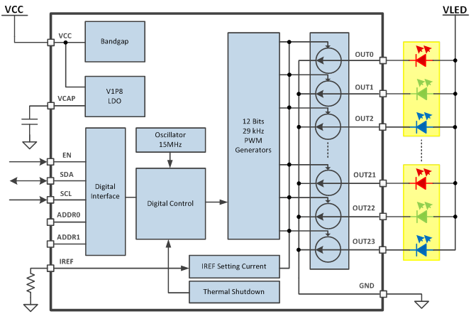
A DLP-technology-based system uses additional sensor input to turn off the part of the headlight that would project onto the windshields of oncoming cars, causing glare discomfort or distraction for other drivers. By using DLP for headlight systems, very detailed control of the pixelated headlight beam is possible, enabling adaptive high-beam functions to help improve visibility and comfort during nighttime driving. Figure 3 shows an example of a system block diagram that includes the DLP chipset in a headlight system.


Figure 3: System block diagram featuring the DLP chipset.


The DLP5531-Q1 chipset for high-resolution headlight systems (Fig. 4) gives engineers a way to control light distribution on the road more precisely through customizable beam patterns in a smaller system form factor. The system also allows for partial or full dimming of individual pixels, potentially supporting consistent usage of high beams without impacting other drivers.


Figure 4: The TI DLP5531-Q1 chipset was developed by TI for high-resolution headlight systems.


Future Uses of Headlight Tech

While many automakers and Tier-1 suppliers are focusing on the benefits of enhancing visibility, DLP technology is also programmable. As a result, it can be configured for the new functionality that will be required by semi-autonomous and autonomous vehicles.

DLP technology for headlight systems can work with ADAS to project the right amount of light on specific spots, such as traffic signs, so that drivers can clearly identify the sign. Its ability to project images and signs onto the road ahead, such as lane markings or navigation directions, will enhance communication between drivers, pedestrians, and other vehicles, a feature that will become more important as the industry moves forward.

Headlight systems using this technology can be programmed to enhance car-to-pedestrian communication by providing signaling or signs to pedestrians and indicating what the vehicle will do next. In addition, dedicated lane marking and enhanced car-to-driver functions like symbol projection and the display of relevant information for drivers (e.g., navigation support, vehicle trajectory) are important considerations for future vehicles.

Additional Specs

The DLP5531-Q1 chipset supports more than 1 million addressable pixels per headlight. Working with any light source (including LED and laser), it operates between -40°C and 105°C, enabling clear image visibility regardless of temperature or polarization.


This content originally appeared on Electronic Design.

QFN soldering tips and tricks

$
0
0

If you’re looking to power a space-constrained, high-power-density, thermally critical application, high-efficiency converters in tiny quad flat no-lead (QFN) packages offer great performance value. But you might ask yourself, when you test and debug your prototype boards, will you be able to handle those minuscule packages in your lab? Will you need special equipment or soldering talent?

No need to worry – it’s much easier than you think! Our lab experts have some hands-on tips and tricks for you.

First, make sure that your board is completely dry – otherwise there’s a risk of printed circuit board (PCB) delamination. Uniformly heat up the board from the bottom using a ceramic hot plate set at ~150°C (you can safely go up to 200°C for larger PCBs with eight layers or more).

To reach the right local soldering temperature, point a hot-air nozzle toward the integrated circuit (IC) landing position on the PCB. Since the IC package temperature should not exceed 260°C per TI specifications, be careful to limit the hot-air temperature.

Once you’ve reached a stable temperature, apply the flux and distribute the solder evenly on the PCB pads (for such small packages, we use lead-free, 0.2-mm solder wire). Hold the IC with tweezers a few millimeters away from the landing pads during the PCB pad pre-tinning process. When the solder is molten on the pads, stop the airflow and drop the IC on the PCB pads (see Figure 1). The IC will self-align to the PCB pads as long as the solder is liquid. Carefully blowing some hot air again will help support the alignment.

Figure 1: Keeping the IC above the landing pads during the pre-tinning process (a); dropping the IC on the PCB pads once the solder is molten and carefully blowing hot air to support the alignment (b)

Try to work as quickly as possible to avoid using up the flux and having the solder oxidize before you’ve properly placed the IC. Of course, pay attention to elementary precautions like working in an electrostatic discharge-safe environment.

That’s it!

When you start working on your next thermally critical design using our new TPS62827, a 2- to 4-A high-efficiency buck converter in a 1.5-mm-by-1.5-mm QFN package, also check out the data sheet, which has specific guidance on how to properly lay out the PCB land pattern, solder mask and solder stencil for this package. In addition, the application note “QFN and SON PCB Attachment” gives a detailed overview of the essentials for ensuring the smooth manufacturability of your board.

Using an RGBW LED driver to elevate LED human-machine interface designs

$
0
0

Smart Home Connected IoT

Products are becoming very intelligent and connected with each other. Devices such as speakers, TVs, refrigerators, set-top boxes and smoke detectors are no longer objects that just sit there – users can control them remotely or through voice wakeup. Devices are much smarter than before, which means they will also require an improved human-machine interface.

A light-emitting diode (LED) indicator like an LED ring, LED matrix or red-green-blue (RGB) LED lighting interacts with users by changing patterns, such as chasing or blinking. Figure 1 shows some pattern examples.

Personal Electronics  RGB LED White LED Drivers  Power Button Control


Figure 1: Examples of LEDs used for a human machine interface

To have a very friendly human-machine interface, these elements are important:

  • Perfect color mixing, with the color changing at the user’s request.
  • Smooth LED brightness: not too dark during the day and not too bright at night.
  • Nice dynamic changing effects, like chasing or blinking.
  • Power efficient in case the power comes from a battery.

While at first this list may seem daunting, all you need to generate great LED effects is a smart LED driver with these key features:

  • The ability to drive multiple channels with a proper communication protocol like I2C. A microcontroller (MCU) could talk to this device and control each channel independently, without consuming a lot of general-purpose input/output.
  • High-resolution pulse-width modulation (PWM) control for changing the brightness of the LEDs.
  • A very low quiescent current, as well as a proper power-saving mode.
  • High-frequency pulse-width modulation to avoid audible noise, since many LED indicators are used with speakers.

TI’s LP50xx family of multichannel, RGB LED drivers, shown in Figure 2, is a good fit with this feature list.

TI LP50xx Family Functional Block Diagram

Figure 2: LP50xx family functional block

The devices integrate a 12-bit PWM generator that operates above a human-audible frequency, at 29 kHz per channel, enabling smooth, vivid color with zero audible noise. 18-, 24-, 30- and 36-channel options provide independent color mixing and brightness control. With an integrated power-saving mode, these LED drivers dramatically reduce power consumption to improve total system efficiency in standby mode.

The LP50xx family enables you to achieve seamless, smooth animation in applications that use a human-machine interface, such as portable electronics, building automation and appliances.

Additional resources

With capacitive touch, liquid is no longer kryptonite to keypads

$
0
0

(Please visit the site to view this video)


It’s no secret liquid and electronics don’t mix, and companies today are spending millions of dollars each year to “water proof” their products. Liquid damage can cause a device to degrade, malfunction or stop working entirely and no amount of hot air or rice can bring it back to life.


The Ingress Protection (IP) code rating system ensures that you know the level at which devices are sealed from the elements. An IPX2-rated product may withstand minor moisture, whereas IPX3 may withstand droplets. An IPX4 rating indicates that the product can tolerate water splashing from any direction, while an IPX5 rating signifies tolerance from streams of water coming from multiple directions. If something has a water-only rating, you write it as IPX; the X acts as a placeholder, since there is no particle rating.


Whether a product is completely submerged or sustains just a couple of drops, receiving the correct IPX rating is important to know the reliability of a device when encountering liquid.


Mechanical push-buttons have drawbacks in products that might be exposed to liquid damage. Water might seep through the mechanical button cutouts to the internals, or there may be extra manufacturing costs to seal the buttons against liquid entering.


Capacitive touch buttons are a more reliable solution. The Liquid Tolerant Capacitive Touch Keypad Reference Design, shown in Figure 1, works properly (no false detections and accurate button-touch detection) with bare fingers under IPX5 water resistance rating conditions. The keypad in this reference design was developed using an MSP430FR2633 CapTIvate™ microcontroller (MCU), which has integrated capacitive touch technology.


Figure 1: Liquid Tolerant Capacitive Touch Keypad Reference Design


The keypad detects a capacitive touch event and provides audio feedback through a “beep” and visual feedback through LEDs. As demonstrated in Figure 2 and the video above, the keypad maintains proper operation even in the presence of running water. If your product operates in an outdoor environment and is exposed to elements such as rain, MSP430™ MCUs with CapTIvate technology can be a reliable and sleek alternative to mechanical buttons.


Figure 2: Capacitive touch keypad with running water


Additional resources

TI brings deep learning inference to the edge

$
0
0
Even if you’re not very familiar with deep learning, you’ve probably heard about it. Whether it’s how it can help bring autonomous vehicles to the roads, challenge the world’s best Go players, increase manufacturing efficiency...(read more)

An open-and-shut case, part 2: advantages of inductive-based case tamper detection in smart meters

$
0
0
In the first installment of this series, I discussed some of the limitations of mechanical tamper detection for smart meters and introduced a new inductive-based implementation using the LDC0851 . In this installment, I will discuss the advantages of...(read more)

Top trends driving the automotive industry in 2019

$
0
0

As 2018 comes to a close, it’s exciting to reflect on this decade as being on the precipice of the biggest evolution in cars since their inception more than a century ago. As autonomous and electric vehicles continue to gain traction, cars in the next decade may look quite different from the cars of the 2010s.

Looking ahead, there are four high-level themes that will drive innovation in the automotive industry in 2019.

Digital cockpit

Vehicle electrification

Connected car

Autonomous driving

Digital cockpit
Enhancing the driving experience begins in the driver’s seat where the driver presides over a central command center, an integrated cockpit

  • A driver can spend as much as 38,000 hours behind the wheel in their lifetime according to Harvard Health Watch. Whether the passenger is driving in the near future or relaxing in a self-driving car in the distant future, the vehicle seats must be comfortable. That’s why all iterations of powered seats will stay relevant in 2019 with customizable features and climate control.
  • Consumers are expecting more dynamic interactions with the cockpit. In 2019, look for more gesture control as a next-generation way to manage controls within the digital cockpit.
  • As the cockpit evolves so does the acoustic nature of the cabin. Premium audio innovations that shape the sound in the vehicle are more in demand, even in base-model vehicles.
  • Selecting the right power topologies will be of even greater importance for the evolution of body control modules that power features of comfort and convenience.

Read the white paper to explore power options: System power architectures in body control modules. 

Vehicle electrification
Government regulations worldwide are challenging automakers to reconfigure and reimagine the powertrain to reduce emissions. A glimpse ahead in 2019, we can categorize the trends into on a three-part spectrum. 

Improving
the overall efficiency
of combustion engines.

Electrifying
mechanical components
to enable hybrids.

Designing
fully
electric vehicles.

Within these categories, key trends have emerged: 

  • More accurate sensors and exhaust-treatment centers will improve the combustion engine process.
  • The standard 12-V battery is increasingly strained with the load of new electronic components. In response, designers can design a 48-V system to add power capacity for starter/generators and traction inverters assisting the combustion engine to reduce emission in Mild Hybrid Vehicles.
  • Gate drivers, amplifiers, data converters, and digital isolation will provide the reliable isolation needed to manage high-efficient on-board chargers, high-voltage battery systems, DC/DC converters and powerful traction inverters in electric vehicles with up to 800 V. 
  • As electric vehicles become more prevalent, there is an increased need for faster charging; innovations to watch is fast DC charging stations up to 350 KW and inductive charging which is considered to be an enabling technology for autonomous transportation services.

Read the white paper and see the reference design: Bridging 12 V and 48 V in dual-battery automotive systems.

Autonomous driving
Encompassing more than fully self-driving cars, in 2019, autonomous driving in passenger vehicles will be experienced primarily through driver assistance functionality, features that are designed to mitigate or prevent human error on the road and improve the situational awareness of the driver.

  • Camera monitoring systems (CMS) will increasingly encroach on the job of traditional mirrors to expand the driver’s view making smart mirrors more common in new vehicles. 
  • Sensor fusion combines information from camera, radar and ultrasonic systems to enhance ADAS features.
  • Cameras inside the vehicle will continue to make progress by providing driver monitoring to detect head and eye position to determine drowsiness or distraction.

Read the white paper to learn more: Paving the way to self-driving cars with advanced driver assistance systems.

Connected car
Modern vehicles are as connected to the outside world as the driver is with their smartphone. Smart driving will become the norm with vehicles communicating with the driver, other cars on the road, infrastructure, the cloud and pedestrians—all while giving passengers the constant connection we’ve come to expect.

  • Vehicle-to-everything (V2X) innovations will continue to advance and gives drivers, passengers and the car itself greater connection than ever before.
  • In 2019, a winner may emerge in the rivalry between Cellular LTE standard driven by 5GAA (C-V2X) and Dedicated Short Range Communication using WiFi IEEE standard, 802.11p (DSRC).
  • Smartphones will become increasingly connected to the car overall, but particularly with car access. In 2019, time of flight technology may allow a car to securely recognize its driver. 

Learn more about telematics in the blog: Four design considerations for telematics hardware in the connected car.

Now it’s your turn. What are the automotive innovations and insights you expect to see in 2019? Comment below. 

Additional Resources:


Small, high-density precision DACs improve performance in laser-drive applications

$
0
0

In laser-drive applications, a major design consideration facing engineers today is implementing higher channel counts in fixed form factors. In this post, I will explore the benefits of using flexible and precise current sources at high channel counts in systems such as optical laser-drive applications, and examine technical documents and devices from TI that enable these benefits.

High-channel-count, high-precision digital-to-analog converters (DACs) such as the DAC80508 enable high-density and accurate current-source solutions where small size and high performance is required. As described in the application note, “High-Density DACs Offer Superior Noise and Accuracy Performance in Laser-Drive Applications,” laser diodes generally require a precisely controlled current to regulate their output power.

It is advantageous for this current to be adjustable because output power of the laser diode can change over temperature. For this reason, you can employ a DAC to dynamically update the forward current. In addition, you will want a low-noise source to reduce the laser output’s noise intensity (a manifestation of instability in the output power).

Current-output DACs that drive hundreds of milliamps in the market today come with some disadvantages: higher noise, thermal dissipation issues, lack of flexibility, etc. These disadvantages can be overcome by using a high-performing, voltage-output DAC with a voltage-to-current converter that can create a high-side current source to drive the laser diode.

Engineers are more frequently designing with higher channel counts in fixed form factors in laser-drive applications, and individual component size is very important to maximize channel density within these systems. The DACx0508 family enables designers to create dense, high-channel-count laser-drive solutions with maximum performance. For example, the DAC80508ZYZFT provides eight 16-bit voltage DAC channels in a 2.4-mm-by-2.4-mm die-size ball grid array (DSBGA) package with a very precise internal reference, providing the smallest 16-bit, eight-channel high-performance DAC on the market today.

The recently released reference design for laser diode applications with precisely controlled current requirements (see Figures 1 and 2) demonstrates a high-side current-source design implementing a multichannel DAC, operational amplifiers and discrete components to highlight overall size and performance for a variety of laser-drive applications.

Figure 1: Component size comparison

Figure 1: Component size comparison

Figure 2: Block diagram from reference design for laser diode applications  with precisely controlled current requirements

Figure 2: Block diagram from reference design for laser diode applications
with precisely controlled current requirements

The reference design has an output range of 200 mA and enables minimal power supply (PVDD) voltage compliance to reduce power consumption and thus enable high efficiency. It also features a low current-noise output, given the low reference noise from the components used.

If you have a laser-drive application that requires small, accurate, low-noise, high-side current-source solutions, consider the DAC60508, DAC70508 and DAC80508 DACs and OPA2376 op amp.

Additional resources

Using smart relay drivers for smart meters, part 1

$
0
0
Utilities deploy an estimated 100 million smart electricity meters around the world annually. The ability to monitor live power consumption and remotely provide or disconnect electric service to customers is a foundational feature for a smart electricity...(read more)

How to use a voltage reference as a voltage regulator

$
0
0

A version of this post was also published on Electronic Design.

Have you ever needed to bias a low-current load and simply didn’t want to add another voltage regulator? Or been in a situation where you need a reasonable level of voltage accuracy, so a simple voltage divider isn’t enough?

For many years, designers used Zener diodes as a simple shunt voltage regulator, as shown in Figure 1. With a single resistor, the device will maintain the fixed voltage determined during the manufacturing process.

Figure 1: A single resistor and Zener diode create a simple voltage rail

A good Zener diode works well, but when you look closely at the data sheet, you’ll see that you need to source more than a few milliamps in order to realize an accurate Zener voltage (Vz). To maintain accuracy, you must choose a low-enough series resistor value to ensure that the Zener reverse bias current (Iz) falls within an acceptable range. As shown in Figure 2, this range may be as high as 5mA, especially with lower-cost, non-temperature-compensated diodes.

Figure 2: Zener diodes typically require a more than a few milliamps to reach Vz

Ohm’s law and Joule’s law dictate the power losses across the shunt resistor, which affects overall system losses and temperatures. As an example, with a 12V input, using a 2.5V Zener diode would require a 1.9kΩ series resistor in order to maintain 5mA (assuming no load current). A 1.9kΩ resistor with 5mA results in a loss of over 47mW across the resistor. With 24V, the losses are over 100mW.

A voltage reference (also called a band-gap reference) provides the same functionality as a Zener diode yet requires far less current to maintain a more accurate voltage. Where a Zener diode uses a single p-n junction with specific doping to create a Zener breakdown voltage, a voltage reference uses a combination of transistors and employs a positive-temperature-coefficient p-n junction in concert with negative-temperature-coefficient transistors to make a zero-temperature-coefficient reference.

The concept and design of a band-gap reference was introduced back in the 1970s by Bob Widlar when he was a power integrated circuit (IC) designer. Although voltage references are often employed because of their voltage accuracy (well under 1%) over temperature and time, advances in semiconductor circuitry, processes and packaging have brought them into new applications.

Wider-tolerance and lower-cost voltage references (1% and 2%) open up their use in applications where they were never before considered, applications where you might be using a Zener diode or voltage regulator. Using a voltage reference in place of a Zener diode is about efficiency and simplicity.

As shown in Figure 3, the voltage across the voltage reference becomes well regulated when Iz is only 50µA. Figure 3 shows characteristics of the Texas Instruments (TI) LM4040 at 25°C, yet the data sheet shows superb voltage accuracy when biasing well below 100µA over ambient temperatures from -40°C to +125°C (this is the extended Q-grade temperature version; the normal industrial temperature range is -40°C to +85°C). Some voltage references operate at an even lower current, such as the ATL431 and LM385.

Figure 3: The TI LM4040 2.5V voltage reference

Using the same 12V example as above, with 75µA for Iz instead of 5mA, you can use a 126kΩ resistor and maintain a more accurate voltage. Using a 126kΩ resistor also enables you to realize a power loss in the resistor under 1mW, which is well below the 47mW loss when using a Zener diode. Of course, when delivering current to a load, you will need to select a lower-value resistor in order to deliver load current while maintaining the needed Iz for regulation over load variations. As shown in Figure 4, simply calculate the current through the shunt resistor (Rs) where Ir = Iz + Iload and then size the shunt resistor (Rs) using Ohm’s law, R = (Vs-Vz)/Ir. Be sure to use the worst-case load current and take tolerances into account when selecting this resistor.

Figure 4: Calculate Rs to accommodate the worst-case load current while maintaining the minimum Iz

By using a wide-tolerance voltage reference like the 2% LM4040E from TI, you can realize a regulation voltage superior to most voltage regulators at a price lower than a typical voltage regulator and on par with a Zener diode. These devices are also available in small SC70 packages. An advantage of using a voltage reference for voltage-regulation applications is their ability to operate over very large voltage ranges; a voltage reference doesn’t care about voltage, only current. By choosing the right shunt resistor value based on the input voltage range and output current, you can support a very wide range with a simple solution.

Figure 5 is an example of using the LM4040 to develop a low-current 5V rail from a 22-25V input to bias the 5V input to a USB controller IC, which only needs 100µA worst case. The resistor value selected takes into account additional bias current for a load not shown. This application can use the lower-cost 2% E version of the LM4040-N device. As you can see, the circuit is very simple and small when using 0402 passives.

Figure 5: LM4040 voltage reference used to develop 5V

Because you need higher current, the shunt resistor will need to be larger in order to dissipate the thermal losses caused by the voltage drop. The maximum current through most voltage references is in the order of 10mA to 30mA, which limits applications.

For higher current, you can employ the same voltage reference with a bias resistor along with an additional transistor to provide the necessary input-to-output voltage drop. A p-channel FET transistor biased directly from a voltage reference can supply much higher current, yet the output voltage (Vout) will vary with load current as a function of the FET’s RDS(on) characteristics. By adding an error amplifier (a single rail-to-rail operational amplifier works well), the circuit shown in Figure 6 senses Vout and compares it to the voltage reference to provide a well-regulated voltage over various changes in load current and temperature.

Figure 6: A voltage reference is at the heart of all voltage regulator circuits

Removing R2 (and shorting R1), the circuit shown in Figure 6 will provide a very well-regulated voltage equal to the voltage of the voltage reference. Voltage dividers R1 and R2 provide a means to adjust the output to any voltage greater than or equal to the reference voltage.

A voltage reference is at the heart of almost all integrated voltage regulators. You might ask, if it’s this easy, why use an integrated voltage regulator at all? One reason is that a voltage regulator also includes circuitry to monitor and limit current to the load, and monitors the temperature to protect the device and load during fault conditions. Although designers can and do design discrete voltage reference-based regulators, it’s often more practical and cost-effective to use one of the many integrated voltage regulators available today.

So the next time you need a low-current rail voltage, consider using a voltage reference.

Incidentally, significant technical advancements have also been made with both linear and switch mode voltage regulators. When trying to develop a low current voltage off of a 5V rail (or higher) Texas Instruments has recently released a broad family of cost optimized and small solution size linear regulators. The new TLV702 regulator seen in Figure 7, supports up to 5.5V input and offers a wide range of voltage options, a shutdown pin, and the family is available in very small packages.

Figure 7: The TLV70 regulator family provides another cost effective alternate to Zener based shunt regulators

From a switch mode regulator standpoint, the industry has also seen significant advances in both low current as well as high current regulator solutions. Much advancement has taken place with self-contained switcher modules which include all of the necessary magnetics and are very handy for creating low voltage rails. These small modules also have the advantage of lower EMI than traditional discrete solutions, mostly based on lower impedance connections between the self-contained high speed switching nodes. Recently they have become very popular for local rail generation based on their ease of use and decreasing cost based on economy of scale.

The TPS8208x buck regulator family is very small (3.0mm X 2.8mm) and produces tightly regulated voltages with output current up to 3A. For input voltages up to 36VDC, consider the LMZM23601. This small 3.8mm X 3.0mm module can produce low voltage rails with currents up to 1A and higher current versions are available.

Choosing the best power regulation solution for a specific application always takes time and effort, and today more solutions than ever are available. Here we described some obvious and some not so obvious design options, each with specific subtle but often critical advantages that vary greatly depending on system application.

Additional resources:


Covering wide analog input measurement for grid protection and control using 24-bit delta-sigma ADCs

$
0
0
In my two previous blog posts on improving data acquisition (DAQ) for grid protection and control, I discussed the need for interfacing multiple analog-to-digital converters (ADCs) to a single processor and using the programmable real-time unit subsystem...(read more)

Designing daytime running lights, part 1: adding one-fail-all-fail LED fault detection

$
0
0

Daytime running lights (DRLs) are becoming more popular in vehicles and are even a requirement in some countries. As I’m sure you can guess, DRLs are on during the day, which requires them to be very bright.

As a designer, you typically have two choices to achieve the desired DRL LED brightness:

  • Increase the number of LEDs in your string, which results in a much higher LED driver output voltage.
  • Use two LED drivers to enable a lower LED driver output voltage.

Automotive Daytime Running Light Dual String LED Driver Reference Design with Current Balancing outlines an effective way to drive parallel strings of LEDs for DRL applications without adding a second LED driver. In the first installment of this two-part series, I’ll take a brief look at this reference design and investigate how to add one-fail-all-fail LED fault detection.

Reference design overview

The DRL reference design uses the current-balancing circuit shown in Figure 1 and the TPS92692-Q1 LED controller, which allows the device to drive parallel strings of LEDs using a single constant-current output. Equal current flows through both LED strings. Note that the reference string must have one more LED than the mirror string to properly bias the metal-oxide semiconductor field-effect transistor (MOSFET). The reference design guide describes the functionality of the current-balancing circuit in more detail.

Figure 1: Current-balancing circuit

One-fail-all-fail LED fault detection

The main purpose of one-fail-all-fail LED fault detection is straightforward: if a single LED is shorted or opened in either the reference or mirror string, all LEDs in both strings will shut off. Although the concept is simple, its implementation requires a bit more thought and brings up two major questions:

  • How is a fault detected?
  • If a fault occurs, how do you shut off all of the LEDs?

How to detect a fault

While not obvious, it’s possible to detect a fault by monitoring the MOSFET drain voltage. There are four different potential types of faults:

  • An LED short in the mirror string.
  • An LED short in the reference string.
  • An open circuit in the mirror string.
  • An open circuit in the reference string.

To understand how to detect these faults, let’s first analyze how the circuit operates under normal operation; see Figure 2.

Figure 2: Current-balancing circuit under normal operation (Vf is the forward voltage of one LED)

Because there is one more LED in the reference string than the mirror string, and the currents IRef and IMirror are equal, you can use Equations 1 and 2 to define VDriver:

    VDriver = (# of LEDs in reference string)  × Vf + IRef × R0          (1) 

       VDriver = (# of LEDs in mirror string)  × Vf + IMirror × (MOSFET RDSon + R0)         (2)

Now you can use Equations 3, 4 and 5 to define VDrain:

                               VDrain = VDriver - (# of LEDs in mirror string)  × Vf          (3)

                      # of LEDs in mirror string = (# of LEDs in reference string) - 1       (4)

Using Equations 1 and 2:

                 VDrain = IMirror × (MOSFET RDSon + R0) = Vf + IMirror × R0      (5)

You can now analyze the circuit under different fault conditions.

An LED short in the mirror string

As shown in Figure 3, with an LED short in the mirror string, there are effectively two more LEDs in the reference string than the mirror string. Equation 6 defines the new VDrain as:

              VDrain = 2 × Vf + IMirror × R0           (6)

Figure 3: LED short in the mirror string

An LED short in the reference string

With an LED short in the reference string, there is effectively the same number of LEDs in both strings. Equation 7 defines VDrain as:

                      VDrain = IMirror × R0        (7)

Figure 4 depicts the condition where an LED is shorted in the reference string.


Figure 4: LED short in the reference string

An open circuit in the mirror string

With the mirror string open, current flows only through the reference string as shown in Figure 5. The operational amplifier (op amp) drives the MOSFET in the mirror string to its fully on state. Equation 8 defines VDrain as:

         VDrain = 0 V          (8)

Figure 5: Open circuit in the mirror string

An open circuit in the reference string

With the reference string open, current flows only through the mirror string; the noninverting input of the op amp pulls to ground. Since the noninverting input is 0 V, the op amp should ideally drive the MOSFET to its off state. However, as a result of input offset voltage, the op-amp output will saturate to either its positive or negative supply rail. This offset typically varies in both magnitude and polarity due to op-amp parametric tolerances and, depending on its polarity, determines which rail the output saturates to.

Figure 6 depicts this situation where there is an open circuit in the reference string.

Figure 6: Open circuit in the reference string

A negative input offset voltage indicates that the inverting input of the op amp is at a higher potential than the noninverting input and the op-amp output would saturate to its negative supply rail. Thus, the MOSFET would be driven to its off state. However, the LED driver will continue to increase its output voltage in order to drive the current through the mirror string – and because the MOSFET RDSon is modeled as a resistor in parallel with the MOSFET drain and source, a small amount of current will be able to flow. This will cause the MOSFET drain voltage to increase until the LED driver triggers an overvoltage condition. According to the TPS92692-Q1 data sheet, the device would stop sourcing current once the OV limit has been hit, the soft-start will be triggered again once the output voltage drops over a set hysteresis and then begin switching. This results in VDrain oscillating between ~60 V and 0 V with a period of the timing that voltage drops over hysteresis plus the soft-start time.”

A positive-input offset voltage indicates that the noninverting input of the op amp is at a higher potential than the inverting input and that the op amp would saturate to its positive supply rail. With an open circuit in the reference string and all of the current flowing through the mirror string, the voltage at the inverting input would be greater than the voltage at the noninverting input, and the op-amp output would saturate to the negative supply rail. This results in high-frequency oscillations at the output of the amplifier, and thus VDrain oscillations between ~30 V and 0 V.

Check back on Thursday to read part two. 

Resources: 

Viewing all 4543 articles
Browse latest View live


Latest Images