Quantcast
Channel: TI E2E support forums
Viewing all 4543 articles
Browse latest View live

Tiny technology, global impact: TI BAW resonator breakthrough creates new electronic heartbeat

$
0
0


Every electronic system has a heartbeat – a clock signal – that helps each component perform in perfect synchronization.

For decades, designers have used quartz crystals to generate this electronic heartbeat. The crystals oscillate, creating a precise rhythm. But when these expensive crystals start to wear down, they can jitter, or jump, impacting their accuracy over time.

Our company is announcing two new devices that incorporate bulk acoustic wave (BAW) resonators as a new type of electronic heartbeat. At 100 microns wide, these tiny timekeepers are smaller than the diameter of a human hair, yet they operate at frequencies much higher than quartz crystals and provide better system performance.

With the advent of 5G communications and the age of big data, high-precision clocking is essential as increasingly massive amounts of data speed between systems around the world.

Our new TI BAW-based products promise to radically improve the performance of internal clocks and accelerate applications ranging from building automation to virtual health.

In the past, BAW resonator technology has been used to filter signals within communications technologies such as smartphones. Our company’s use of this technology to provide an integrated clocking function is an industry first.


 Learn more about TI’s new BAW resonator technology. 

No quartz needed: Introducing the industry’s first crystal-less, wireless MCU

Our new products include the industry’s first crystal-less wireless microcontroller (MCU), which integrates a TI BAW resonator within the package. This MCU will allow design engineers to create simpler, smaller designs while increasing performance and lowering costs. It will also speed time to market, since designers will be able to eliminate the process of selecting, calibrating and installing external quartz crystals.

“A critically important innovation is the ability to move and analyze massive amounts of data to make accurate, informed decisions,” said Ray Upton, our vice president of connected microcontrollers. “Wireless networking is at the core of this data migration, and the ability to bridge the last mile through connected devices is a vital part of the data cycle.”


By 2022, spending on IoT applications is expected to reach $1.2 trillion, up from an estimated $151 billion in 2018.* This rapid growth indicates that the Internet of Things is penetrating deeply into many markets, with 90 percent of business executives in technology, media, and telecom saying IoT is central to their business strategy.**

Our newest SimpleLink™ multi-standard MCU with TI BAW technology can be integrated into low-power radio-frequency devices, such as crystal-less Bluetooth® low energy and Zigbee® technologies to reduce radio-frequency performance issues created by external crystals.

Clean your clock: TI BAW-based network synchronizer eliminates digital noise

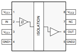
Our other BAW-enabled product is a TI BAW-based network synchronizer, which can be used in combination with quartz crystals to remove digital noise – or jitter – from input signals in the communication sub-system of wired or wireless infrastructure hardware in data center core networks. This will benefit telecom systems such as 5G networks.

“The clocking requirements of tomorrow’s communications infrastructure extend beyond the capabilities of devices that today feature quartz crystal-based resonators,” said Kim Wong, our vice president and general manager of high-speed data and clocks. “By integrating TI BAW resonators directly into clocking devices, we can deliver the ultra-low jitter performance and resiliency against vibration and shock demanded by the growing pipeline of data at the heart of this communications transformation.”

How these tiny timekeepers work

Our TI BAW oscillator is an electronic oscillator circuit that uses the mechanical resonance of a vibrating micro-acoustic resonator (BAW) to generate a stable electrical signal through the piezoelectric effect. This precise signal at very high frequency provides the clocking and timing reference for electronic systems.

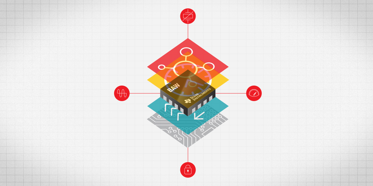
TI BAW-based products offer design engineers several advantages:

  • Smaller form factor. Because they’re integrated into chip packages, circuit designers will no longer need to use separate clocking devices mounted on circuit boards.
  • Lower power in most cases. Many IoT applications require clocking systems to turn on quickly. The TI BAW-based oscillator wakes up 100 times faster than quartz crystals.
  • A lower level of digital noise. Our network synchronizer chip delivers a jitter performance better than the best-performing device on the market today.
  • Cleaner clock. The TI BAW resonator offers an ultra-clean clock reference, which is essential for high-speed data transfers of hundreds of gigabits per second. It also can be integrated with a radio frequency (RF) chip as a single-chip radio solution.

The heart of the matter

As 5G networks and future-generation communication technologies emerge, the implications will range from business and commerce to health care, agriculture and education.

Once the communications infrastructure is in place to support the transmission of huge amounts of data, companies and governments will want to provide a wireless overlay to connect point-to-point over the last mile, from objects communicating with each other in a warehouse to communication between smartphones and thermostats, heartrate monitors and a host of other devices.

“Our TI BAW resonator technology will pave the way for the next generation of industrial and telecommunication applications by changing how we approach system designs,” Ray said.

Next week on Think. Innovate, look for Chief Technology Officer Ahmad Bahai’s column about how this innovation will impact our world.

* Forbes.com: Roundup Of Internet Of Things Forecasts And Market Estimates, Dec. 2018
** Forbes.com: Roundup Of Internet Of Things Forecasts And Market Estimates, Dec. 2018


20 million GaN reliability hours and counting

$
0
0

My advice is to get involved and get started,” — Jack Kilby

About 20 million reliability hours ago, we built our first gallium nitride (GaN) application board in TI’s Kilby Labs. We watched the oscilloscope in anticipation and were amazed at the textbook-like switching waveforms. Power GaN was at an early stage of technology maturity but showed tremendous promise. Integrating a driver and protection features would indeed make the perfect power switch. We knew there was lot of work ahead, so we took Jack Kilby’s advice.

Our early evaluation marked the start of a reliability journey, as we realized that traditional silicon qualification was not testing for hard switching. Many power-management applications hard-switch the field-effect transistor (FET), making this finding very relevant. Hard-switched circuits include buck and boost converters, power factor correction circuitry, inverters and motor drives. Hard-switching stresses the device in a different way, since it includes a brief moment where the device is subject to simultaneous high voltage and current as described in our white paper, “A comprehensive methodology to qualify the reliability of GaN products.”

We realized that the devices needed to be made robust to hard-switching. The methodology in use for silicon was not applicable to GaN, so we started hard-switching the FETs in a boost-converter test vehicle as part of our device development program. This issue of application robustness quickly became known in the industry, along with the need to collaborate, as described in our blog post, “Let’s GaN together, reliably.”These aspects catalyzed the formation of the Joint Electron Device Engineering Council (JEDEC) JC70 committee on wide bandgap power electronic conversion semiconductors, and have accelerated the availability of reliable GaN.

Reliability is our highest priority, and we knew that the release of a reliable technology to manufacturing encompasses much more than hard switching, as illustrated in Figure 1. The LMG341x family of devices has both reliable GaN and silicon, is manufacturable, incorporates protection features, is integrated into a low-inductance package, and is validated to work robustly in applications. These device features were achieved with coordinated efforts in device reliability, application robustness and manufacturability, in addition to considerable accelerated stress testing and failure analysis.

Figure 1: A methodical path to the manufacture of high-quality dependable products. In addition to substantial reliability effort in device engineering, application robustness and manufacturability programs, the LMG341x device also has design-for-reliability features and benefits from our participation on the JEDEC JC70 committee

We take successful designs through a standard qualification procedure, involving both GaN-only and LMG3410 devices. Nowhere is Thomas Edison’s quote, “Genius is 1% inspiration and 99% perspiration,” more true, and we have certainly made our devices perspire in hot and humid chambers. We have conducted over 20 million hours of reliability testing, as shown in Figure 2, broken down into four categories: manufacturing, application robustness, GaN device reliability and JEDEC qualification.

Figure 2: Pie chart showing the breakdown of the various categories of reliability testing hours

It’s easy to see how the reliability hours accumulate. GaN device reliability is designed through the understanding of the time-dependent breakdown failure mode, field plate engineering, the judicious choice of appropriate materials and thicknesses, and by engineering the epitaxially grown layers. We run large quantities of regular devices and special test structures specially designed for understanding failure mechanisms, testing 10,000 wafer-level structures and 8,000 packaged devices to build comprehensive reliability models and predict device lifetimes. Our model shows that the overall FET and high-field-withstand components have lifetimes of over 100 years.

We also tested devices for stable dynamic RDS(on) and hard-switching safe operating areas by routinely running them on application reliability test boards for 1,000 hours. Dynamic RDS(on) is a measure of the on-resistance that power-supply designers see during product operation and is a consequence of charge trapping by high fields. Dynamic RDS(on) reliability engineering consists of optimizing interfaces, developing in-process cleans that leave pure surfaces, depositing high-quality dielectrics and optimizing growth parameters of the GaN epitaxial layers. We test the multichip module (MCM) at the system level using our customer evaluation module card to ensure that there are no effects from the interactions of the components or in other modes of operation, such as synchronous rectification. We also test the MCM for extreme conditions like short circuits and lightning surges.

Manufacturability and use of the mature silicon infrastructure also forms a key part of our program. Silicon manufacturing processes are very cost-efficient, not only in wafer processing, but also in the packaging process of wafer thinning, die singulation and assembly. In order to develop good GaN manufacturing, we have run over 10,000 devices in burn-in boards, both for early failure detection and for longer-term high-temperature reverse-bias validation testing. We have also run the well-proven traditional (JEDEC) qualification on both the intrinsic technology and the product, including extending the major tests to 2,000 hours, double the regular stress time.

With 20 million hours of stress testing behind us, there are now many good reasons to find out more about the perfect power switch at http://www.ti.com/GaN.

Three low-side LED biasing topology options and their trade-offs

$
0
0

Many imaging products are moving toward more efficient LED array-based solutions and away from traditional technologies such as lasers or lamps. Applying resistive voltage dividers enables the linear forward biasing of LEDs for proper operation. However, because the biasing point of any LED can change across temperature – as well due to actual device-to-device variability – programmability of the particular biasing point then becomes a requirement in precision circuits.

Utilizing digital potentiometers (DPOTs), pulse-width modulation (PWM) or precision digital-to-analog converters (DACs) are common approaches for solving the biasing point programmability. But such solutions also need to be low-cost, small sized and include a high level of integration. Selecting the right architecture then becomes a nontrivial issue. In this blog post, I will discuss the different low-side LED biasing topology options and their respective trade-offs.

DPOT-based biasing

LEDs are usually biased with current; Figure 1 illustrates the most basic implementation of a programmable current source using a typical DPOT with an adjustable shunt reference. Varying the voltage across the Zener changes this circuit’s current. While the Zener approach is effective, a major drawback is that it requires additional components that leads to an increased bill of materials (BOM), footprint and ultimately cost – which is especially pronounced when biasing an array of LEDs. Further, the base-to-emitter voltage (VBE) of the transistor can also vary with temperature and collector current, which can be further undesirable to the design.

DPOT-based biasing

Figure 1: DPOT-based biasing

PWM-based biasing

It is also possible to use a PWM signal instead of a DPOT and Zener to program the bias point. In such cases, the bias point corresponds to the DC value of the PWM signal. While simple to implement, such a circuit also requires one PWM generator per channel, which may be difficult to support depending on what microcontroller you’re using (if any). Another consideration is that a continuous PWM also creates potential distortion and electromagnetic interference-related issues.

A simple biasing method using a precision DAC

Another way to solve the biasing point programmability is to use a simple precision DAC to provide the biasing circuit. Figure 2 depicts this configuration, including the use of the 10-bit, 8-channel, buffered-voltage-output DAC53608. This approach provides a circuit with the smallest size and lowest BOM cost.


Start your next design with an easy-to-use platform

 Quickly and easily demonstrate the functionality and versatility of the 10-bit, 12C interface, buffered-voltage-output DAC53608 with the evaluation module. Learn more.

Keep in mind, however, that like the previous circuit, drift can exist within the VBE of the transistor, and the output may also require some headroom near the ground rail due to the expected VBE drop.

Programmable LED biasing circuit

Figure 2: Programmable LED biasing circuit

While the VBE can vary with temperature and collector current, you can ignore such variations in applications that place the circuit inside a larger feedback loop with gain. With that said, there may be concern for applications that are open loop and that do not employ temperature calibration. The drift in VBE due to temperature and collector current can lead to gain error and full-scale error at the system level.

A robust way of compensating for such VBE variation is to place the circuit inside the feedback loop of an amplifier, as shown in Figure 3. This circuit is very suitable for applications that require high accuracy; the only drawback is the additional amplifier.

 Vbe compensation using buffer

Figure 3: VBE compensation using buffer

Figure 4 shows yet another approach for compensating VBE: using a matched pair of P-channel N-channel P-channel and N-channel P-channel N-channel transistors to cancel out the voltage variations and any headroom. As you can see, this circuit helps balance the benefits of accuracy, solution size and cost.

Vbe compensation without buffer

Figure 4: VBE compensation without buffer

Table 1 compares each topology. The precision DAC-based solution stands out over the other approaches in many aspects. General-purpose precision DACs in 8- and 10-bit resolutions have been flooding the market for a long time, but the DAC53608 (and its device family) provides the latest semiconductor technology to enable easily implemented, smaller, ultra-low-cost LED biasing solutions.

Comparison table of LED biasing toplogies

Table 1: Comparison of LED biasing topologies

The DAC53608, first in a family of small DACs, is an eight-channel buffered-voltage-output DAC packaged in a tiny 3-mm-by-3-mm QFN package. It offers single-supply operation and also comes in an 8-bit pin-compatible version, the DAC43608. These DACs provide an I2C interface whose device address can be configured for up to four different values using a single hardware pin, which allows the use of as many as 32 channels without the need for an I2C buffer.

Could the DAC53608 be part of your LED-biasing circuit design?

How to achieve fast frequency hopping

$
0
0

Frequency hopping describes a method in which communication systems rapidly change their operating frequency for purposes specific to their application. Applications such as communications, radar and electronic warfare use frequency hopping in order to avoid interference or detection, or to detect cloaked signals. The faster these systems can change frequencies – or frequency hop – the more agile they become, making it easier to avoid interference and detection.

Traditional frequency hopping uses an analog mixer and a phase-locked loop/voltage-controlled oscillator, and changing frequencies can take quite a long time. As radio-frequency (RF) sampling has become more prevalent, frequency hopping has moved toward a numerically controlled oscillator (NCO)-based hopping technique; however, the frequency hop time can still be limited by a slow Serial Peripheral Interface (SPI) and the multiple register writes required to update the NCO. Figure 1 shows a typical complex digital mixer with a single NCO.

Figure 1: Complex mixer with a single NCO

Figure 1: Complex mixer with a single NCO

In this blog post, I’ll introduce a technique that enables faster frequency hopping using an architecture with multiple NCOs.


Design for faster frequency hopping

 Learn more about the frequency hopping capability of the AFE7444 and AFE7422 in our application note.

First, let’s look at how long it takes to update the frequency with a single NCO. Figure 2 shows the time it takes to reprogram transmitter (Tx) NCO0 from 10 MHz to 100 MHz. The yellow signal shows DAC A in direct digital synthesis (DDS) mode, where the frequency of the signal is the active NCO frequency. Each falling edge in the blue signal represents the start of a single SPI write. Updating the transmitter NCO frequency requires seven SPI writes. As you can see, updating the frequency of Tx NCO0 from 10 MHz to 100 MHz takes about 4.6 µs, with a maximum SPI clock of 40 MHz.

Figure 2: Updating the frequency in one NCO takes about 4.6 µs

Figure 2: Updating the frequency in one NCO takes about 4.6 µs

It is possible to achieve faster frequency hopping with multiple frequency-flexible NCOs, as opposed to reprogramming one NCO. When multiple NCOs are available, you can program the NCOs that are not selected to different frequencies in the background via SPI while the currently selected NCO is active. When it’s time to change frequencies, you only need to change the selected NCO.

Figure 3 gives an example of this method using TI’s AFE7422. In the AFE7422, each receiver (Rx) contains four available NCOs in dual-band mode and three available NCOs in single-band mode. Rx NCO0 and Rx NCO1 are loading the center frequencies of the blue and red bands in the input spectrum, respectively, while Rx NCO2 is currently selected to downconvert the green band in the input spectrum. Hopping to a different-colored band only requires sending a command to select an already-programmed NCO to the desired band’s frequency, greatly reducing hop time.

Figure 3: Example of frequency hopping with multiple NCOs

Figure 3: Example of frequency hopping with multiple NCOs

It takes much less time to change NCOs than it does to reprogram a single NCO.

Figure 4 shows the time it takes to switch from Tx NCO0, programmed to 10- MHz, to Tx NCO1, which is also programmed to 10 MHz. The yellow signal shows DAC A in DDS mode, where the frequency of the signal is the active NCO frequency. Each falling edge in the blue signal represents the start of a single SPI write sent to the device. One SPI write is required to switch NCOs, reducing the hop time from 4.6 µs to approximately 660 ns.

Figure 4: The hop time when switching from one NCO to another is approximately 660 ns

Figure 4: The hop time when switching from one NCO to another is approximately 660 ns

In the AFE7444 and AFE7422 receivers, it’s possible to switch NCOs using a general-purpose input/output (GPIO), which takes even less time. While switching NCOs via SPI takes about 660 ns, Figure 5 shows the time it takes to switch from an Rx NCO programmed to 100 MHz to an NCO programmed to 10 MHz using a GPIO. At time t = 0, the GPIO pin is triggered to switch NCOs; as you can see, it takes less than 300 ns to switch from one NCO to another.

Figure 5: Rx NCO switching via GPIO; at time t = 0, GPIO is triggered, and the hop time is about 300 ns

Figure 5: Rx NCO switching via GPIO; at time t = 0, GPIO is triggered, and the hop time is about 300 ns

More NCOs available in a frequency-hopping system enables more selectivity when executing fast frequency hopping. The receiver digital downconverter (DDC) multiplexer is an optional feature available on the AFE7444 that uses the fast-frequency-hopping technique for multiband selectivity. Figure 6 illustrates how the DDC multiplexer feature works.

Figure 6: DDC multiplexer feature illustration

Figure 6: DDC multiplexer feature illustration

With the receiver DDC multiplexer feature enabled, a single analog-to-digital converter (ADC) with an instantaneous bandwidth of 1,200 MHz digitizes an analog input spectrum and outputs the digital data to both of the multi-DDC blocks within the same Rx pair. (ADC A and B represent the first receiver pair and ADC C and D represent the second receiver pair). Turning off the unused ADC in the pair can save power. Using this feature in dual-DDC mode, where both DDCs are active in each ADC, shows just how selective the AFE7444 and AFE7422 receivers can be when frequency hopping.


The AFE7444 is configured in dual-band mode, where each ADC can selectively send two bands at a time to a digital processor. ADC A samples the entire input spectrum containing the multicolored, 200-MHz-wide bands. The digitized spectrum at the output of ADC A is then routed to the multi-DDC input of both ADC A and ADC B, while ADC B is turned off to save power. Each receiver NCO within each multi-DDC mixer is then programmed to the center frequency of a distinct band within the spectrum. The color of each receiver NCO identifies which band will be selected within the input spectrum. In total, each ADC pair within the AFE7444 or AFE7422 can pass up to four bands (out of eight bands) without updating the receiver NCO frequency.

If you’re ready for fast frequency hopping, check out the AFE7444 and AFE7422. These quad- and dual-channel RF-sampling transceivers enable the direct sampling of input frequencies into the C band without the need for additional frequency-conversion stages.

Gain ultra-high power density for 100-W USB Power Delivery adapters

$
0
0
The USB Power Delivery (PD) standard enables power delivery via USB up to 100 W, which is sufficient enough to drive high power rated devices like laptops, monitors and DLP® movie projectors. USB PD adapters traditionally use an inductor-inductor...(read more)

Disruptive TI BAW technology accelerates big data on the information superhighway

$
0
0


Imagine the possibilities: A newborn with a heart condition is able to go home with her family rather than remain in the hospital because the doctor can check her vital signs in real time over a wireless network. Or a farmer uses augmented reality to remotely monitor his livestock or inspect the condition of his fields.

Sending and receiving enormous amounts of data wired or wirelessly has a significant impact on our lives every day and fuels the economy in a highly connected world. And technology is crucial for unleashing these opportunities.


 Learn more about TI BAW resonator technology

Data has become a universal need

Much like the 20th century was the era of oil and commodities, the 21st century is the era of big data. In a world of billions of connected people and tens of billions of connected machines, the flow of data is growing exponentially. And there’s no end in sight.

From virtual health and smart agriculture to smart cities and intelligent factories, billions of new electronic devices will connect and become sources and consumers of massive amounts of data. Terabytes of data generated by sensors in factories are analyzed every day to improve the efficiency of production lines. Data collected by semiautonomous vehicles today will enable more autonomy in the future. Automated buildings will help us increase productivity and make our lives greener.

The communications and data-processing infrastructure will make data useful, actionable and valuable to leaders in these markets and billions of other people who are traveling down the information superhighway.

In the not-so-distant future, if you don’t have access to data you will be as limited as if you didn’t have access to electricity.


Timing reference

Data is represented by bits and symbols. And just as each musician in a symphony must play in tune and in sync with the other players – all directed by a conductor – a stable clock and timing reference is critical to synchronize the generation and transportation of bits and symbols.

As high-speed data travels on a cable across town or under the ocean, from one rack to another in a data center, over the ether in wireless systems, or just across a high-speed circuit board, it needs to be synchronized or reconstructed using a very clean timing reference. If the edges of the clock signals aren’t precise, the analog signal may be sampled at the wrong moment. Or if the frequency of an RF receiver is not stable, the received signal may not get demodulated properly.

New technology puts time on your side

For generations, a quartz crystal resonator has been used as a reference for time and frequency in electronic systems. However, that approach can be costly, time-consuming and complicated to develop. It also can be susceptible to environmental stress.

Our disruptive new TI bulk acoustic wave (BAW) technology will provide a much cleaner clock reference for wired and wireless systems. Operating at orders of magnitude higher frequency than quartz crystals, the TI BAW resonator generates a stable electrical signal through the piezoelectric effect. The periodic signal at very high frequency provides the timing reference.

Our TI BAW-based technology enhances the performance and ease of use of wireless solutions supporting standards such as Zigbee®, Bluetooth® low energy and Wi-Fi® and paves the way for the next generation of ubiquitous connectivity.

Learn more: Ahmad Bahai explains how our TI BAW technology paves the way for high-speed connectivity.

TI BAW resonator innovation puts time on your side

$
0
0

Our CTO, Ahmad Bahai, explains our breakthrough TI BAW resonator technology and how it paves the way for high-speed connectivity.

Every RF, mixed-signal and digital system needs a timing and clock subsystem to synchronize the generation and transportation of data. Data transfer rates in a wired network or on an FPGA board have risen from hundreds of megabits to hundreds of gigabits per second. Similarly, the data rate of wireless networks supported by communication standards such as Wi-Fi® and Bluetooth® low energy have grown exponentially.

Historically, a quartz crystal resonator has been used as a reference for time and frequency in electronic systems. Quartz resonator frequencies range from a few kHz to a few MHz.

Our disruptive new TI bulk acoustic wave (BAW) technology offers a much cleaner clock reference for wired and wireless communication systems. Resonating at much higher frequency – about 2.4 GHz – it can provide a cleaner reference for a radio system or high-performance clock distribution.


TI BAW resonator technology


Learn more about TI BAW resonator technology

TI BAW technology:

  • Is capable of generating an ultra-clean clock reference, which is essential for data transfers of hundreds of gigabits per second.
  • Can be integrated into any type of TI chips that require a timing reference. Integrating the TI BAW-based frequency reference can significantly reduce the complexity and cost of designing an RF board with an external frequency reference.
  • Wakes up fast. Many Internet of Things applications operate intermittently, which requires clocking systems to turn on quickly. TI BAW-based technology wakes up orders of magnitude faster than quartz-crystal-based clocks. This provides a power benefit for low duty-cycled operation.

Learn how TI BAW technology accelerates big data on the information superhighway.

What’s with chirping smoke detectors?

$
0
0

Most homeowners and apartment dwellers can relate to being woken up in the middle of the night by a chirping smoke detector that needs a new battery. Usually, the smoke detector is installed in a hard-to-access location, so silencing the alarm involves engaging in acrobatics with a broomstick or some other similar object.

Why do smoke detector batteries seem to drain so quickly, especially for a device that is asleep most of the time? The vast majority of smoke detectors are designed to be relatively compact and cost-effective, with a singular purpose of detecting smoke and heat in proximity. Smoke detector designs implement an array of sensors connected to a processor; that processor uses a small battery as its power source to trigger audible and visible indicators. Smoke detector designs need to be kept relatively simple in order to keep costs down and make them easy to install.

One way to keep things simple is to outfit smoke detectors to accept readily available battery types such as 9-V alkaline and lithium batteries. These batteries are inexpensive to replace, but they are not designed to last very long. In order to stretch battery lifetimes as long as possible, smoke detector designs try to implement internal circuits that balance both cost and low current leakage.

One common approach engineers take to lower implementation costs is to use discrete components such as field-effect transistors (FETs), resistors and capacitors in their circuit implementations. The trade-off of discrete components has always been higher current leakage and increased board space usage. Now, however, new ultra-low-power building-block circuits are enabling design engineers to implement very-low-power designs with cost-effective solutions housed in the latest small-footprint packaging technologies.

One example of a device that can replace discrete components without having to compromise the design is the 2N7001T, TI’s newest 1-bit unidirectional voltage-level translator. Voltage translators are essential when interconnecting devices like sensors to the low-power processors used in smoke detector designs, as seen in Figure 1. The 2N7001T enables designers to improve battery life compared to discrete level-translation solutions by dramatically reducing the current leakage associated with low-cost discrete FET and resistor components.

Figure 1: Residential smoke and heat detector design block diagram

The 2N7001T consumes and maximum of 8 µA in partial power-down mode and 16 µA during operation. The Ioff protection circuitry of the 2N7001T ensures that no excessive current is drawn from or to an input, output or combined input/output, which is biased to a specific voltage while the device is powered down.

In comparison, common discrete level-translation implementations consist of multiple components where each component contributes to the leakage of the circuit, as shown in Figure 2. Discrete circuits such as these can consume multiple milliamps as a result of current leakage.


Figure 2: Discrete push-pull level-translation implementation

Depending on the components selected, the leakage can be even higher for discrete implementations. Given the always-on nature of discrete implementations, they can greatly reduce the battery life of the applications in which they’re used.

The other consideration for using an integrated solution like the 2N7001T is implementation size. Since the 2N7001T is a single-component solution housed in a small package, it’s possible to implement the level-translation function using a minimum amount of board space. Comparatively, the discrete level-translation implementation shown in Figure 2 requires four components and a much larger amount of board space to the implement the circuit.

Figure 3 compares the size of the discrete implementation to the 2N7001T implementation.


Figure 3: Size comparison between discrete push-pull level translation (left) and the 2N7001T implementation

With the benefit of lower power operation and reduced board-space usage, devices such as the 2N7001T can enable longer battery life and smaller form factors while keeping costs contained for applications like smoke detectors. For more information about the benefits of the 2N7001T, see the “Common Risks of Discrete FET Voltage Translation and Advantages of TI’s Integrated 2N7001T Level Shifter” application note.


Power to the pedal: Achieving longer-lasting 13S, 48-V lithium-ion battery packs for e-bikes and e-scooters

$
0
0
The rise in popularity of e-bikes and e-scooters demands an increasing need for longer-lasting e-bike/e-scooter battery packs. A longer run time allows for further travel and less frequent charging. To achieve longer-lasting lithium-ion (Li-ion) batteries...(read more)

What are isolated digital inputs?

$
0
0

Although they might sound similar, there are actually some noteworthy differences between isolated digital inputsand digital isolators. After reading this post, I hope it will be easy for you to tell the differences between the two isolation functions.

Internal structure

Digital isolators serve the basic (or often reinforced!) function of providing galvanic isolation digital signal paths. TI isolation structures are capacitive, with the insulation barrier consisting of two high-voltage capacitors built from our complementary metal-oxide semiconductor (CMOS) process technology. A high-frequency carrier communicates across the isolation barrier from the primary side to the secondary side, and our digital isolators are capable of withstanding up to 12.8 kV of applied surge voltage and 1.5 kV of working voltage without breaking down the double capacitive barrier. A key component of digital isolators is the isolation rating of basic or reinforced.


Isolated digital input

Figure 1: Digital Isolator

Isolated digital inputs serve the basic (yes, basic!) function of providing galvanic isolation from a sensor input or other input type to a logic output for a host controller interface. Unlike digital isolators, the input stage of an isolated digital input (shown in figure 2) includes a user-set input threshold and integrated current limit that allows input voltages ranging from 9V to 60V to be translated to a logic output. In its simplest form, isolated digital inputs operate as isolated comparators, with some great added features for ease of design.

Diagram of an isolated digital input

Figure 2: Isolated Digital Input

Use differences

Digital isolators are typically used between analog-to-digital converters (ADCs) or data-acquisition converters and a host controller or microcontroller (MCU) in the signal path. Digital isolators are also commonly found in the isolated power-supply functions of a given system.

Isolated digital inputs are designed specifically as digital input receivers for programmable logic control (PLC), motor control and grid applications to interface between field-side inputs and a host controller. Isolated digital inputs are field-side facing inputs that are easily configurable for sinking and sourcing applications. An integrated current limit minimizes the thermal profile of the input in higher input-voltage environments and is set with a simple external resistor for compliance to International Electrotechnical Commission (IEC) 61131-2 switch types 1, 2 or 3. An additional resistor sets the input-voltage threshold; an online calculator is available to make resistor selection easy


Power differences

Digital isolatorsrequire both primary- and secondary-side power. In Figure 3, an isolated power supply powers the ADC and the “field side” of the digital isolator interfacing the ADC.


ISO7741 in communication diagram

Figure 3: ISO7741 isolates MCU and ADC communication

Isolated digital inputs require secondary-side power only. In the ISO1211 (Figure 4) and the ISO1212 isolated digital inputs, the field side is powered from the input, so no field-side power is needed. This makes for a simpler design on the front end compared to alternative discrete solutions.

Figure 4: ISO1211 configured for PLC Digital Input Module 

Our new isolated digital inputs are one example of some of the innovative ways that TI is making the world’s most robust and reliable isolation solutions easier and more efficient.

Additional resources

Top 6 design questions about I2C isolators

$
0
0

Become an isolated I2C expert with our design challenges FAQ. These insights are based on frequently asked questions from the TI E2E™ Community about I2C isolators. We hope this information provides actionable details for engineers working to isolate signals and power in their designs.

1. When is isolating I2C necessary?

Isolation prevents DC and unwanted AC between two parts of a system, while still enabling signal and power transfer between each part. Isolation typically protects electrical components or humans from dangerous voltage and current surges; isolation for human safety is called reinforced isolation. I2C has become a popular global standard in many systems; thus, isolated I2C has spread to most high-voltage markets.

Common isolated I2C applications include:

  • Microcontroller (MCU)-to-MCU communication in network and server power supplies.
  • MCU to analog-to-digital converter communication in automotive battery management systems and medical systems.
  • MCU-to-power-sourcing-equipment controller communication in Power over Ethernet systems.
  • MCU communication with current-/power-monitoring systems.

2. Is it possible to connect two unidirectional channels on digital isolators to achieve a bidirectional channel for I2C communication?

No, connecting two unidirectional channels in opposite directions back to back will not yield a bidirectional channel. If you replace an isolated I2C device with a digital isolator, the digital isolator would latch to a single state and become unresponsive. External components are necessary to implement an isolated I2C bus using digital isolators. For more information on how to implement isolated I2C with a standard digital isolator, see the Analog Design Journal article, “Designing a reinforced isolated I2C bus interface by using digital isolators.” Additionally, this E2E Community Isolation forum thread goes into more detail as to why a digital isolator will latch to a single state when used without external components in a bidirectional I2C application.

3. What is the current consumption of ISO1540 and ISO1541isolated I2C devices?

Table 6.10 in the ISO154x data sheet lists the current consumption of the ISO1540 and ISO1541 without any pull-up resistors. When you add a pull-up resistor, there will be additional current drawn from the resistors. For example, with a pull-up resistor added to the device of 1 kΩ at SDA2/SCL2 and 10 kΩ at SDA1/SCL1, with VCC1 = VCC2 = 5 V, the additional current consumed by the pull-up resistors will be ~5 mA for SDA1/SCL1 and ~0.5 mA for SDA2/SCL2.

For isolated I2C applications requiring even lower power consumption, the ultra-low-power ISO7041 can replace the ISO7731 device, as described in the Analog Design Journal article mentioned in question No. 2. The ISO70xx power consumption will be an order of magnitude better than ISO77xx devices.

4. What recommended logic high and low input voltage levels can be applied to ISO1540 and ISO1541 isolated I2C devices?

Table 1 lists the recommended logic input voltage levels for ISO1540 and ISO1541 devices for Side1 and Side2 inputs.

Side1

 Side2

VIL1< 0.5 V

VIL2< 0.3*VCC2

VIH1> 0.7*VCC1

VIH2> 0.7*VCC2

Table 1: ISO154x Input Voltage Levels

These input voltage levels apply to both the I2C data and clock signals. For more information, see Table 6.3 in the ISO154x data sheet.

5. Why is the logic-low-level output voltage, VOL1, up to 0.8 V on Side1 of ISO1540 and ISO1541 bidirectional I2C isolators?

To achieve the bidirectional functionality of an isolated I2C device, the device needs to be designed with two unidirectional channels connected back to back to achieve a single bidirectional channel. Connecting the two unidirectional channels back to back directly would lead to a lockout situation, where both channels are low. To avoid this, a diode at the output of Side1 makes the low output of the output channel on Side1 look like a high for the input channel of Side1. Figure 1 shows the diode placement.

Figure 1:  ISO154x Simplified Schematic

VOL1 will have a voltage of up to 0.8 V because of this diode. When Side2 sees a low on Side2, Side1 will turn on the field-effect transistor, allowing the diode to conduct, generating a nonzero forward voltage. The thresholds in the ISO154x device are carefully designed to make sure that the bidirectional channel operates smoothly – as long as the VOL and VIL specifications fall within the thresholds of the ISO154x device shown in Table 6.9 of the ISO154x data sheet. This approach has been a common practice in the industry for achieving bidirectional I2C function. A nonzero voltage of logic level low will still be compatible with I2C specifications.

Note that this only applies to VOL1. Since Side2 of the device does not require a diode, the VOL2 will be 0.4 V max, which is common in most digital isolators.

6. How do you generate isolated power for an I2C isolator?

There are several options to generate isolated power for an I2C isolator; the best solution depends on the specific application needs.

One option is to use a transformer driver like the SN6501, which operates in a push-pull configuration with a transformer and optional rectifying low-dropout regulator on the secondary side (Figure 2). The SN6501 is capable of delivering as much as 1.5 W to provide isolated power. This device has the flexibility for use in almost all applications because the transformer and turns ratio can provide the necessary isolation rating and output voltage for the power supply. You can use the SN6505 instead of the SN6501 for as much as 5 W of output power if you need isolated power for additional devices. The SN6505 also has extra protection features such as overload and short circuit, thermal shutdown, soft start, and slew-rate control, enabling a robust solution.

Figure 2: Isolated I2C solution for signal and power with ISO1541

Another option for space-constrained applications is the ISOW78xx family of devices, which provides signal and power isolation in a small-outline integrated circuit 16-pin package. The ISOW7842 can also be combined with external components. Figure 3 shows an example solution for a system with bidirectional data and a unidirectional clock, which when modified with a few extra components can support bidirectional data and clock signals.

Figure 3: Isolated I2C solution for signal and power with ISOW7842

For more information about the advantages and drawbacks of each isolated power option, see “How to Isolate Signal and Power for Isolated I2C.”

What questions did we miss?

If you’re looking for more information about I2C isolators or have a question you would like to see added to this list, leave a comment below and help keep the conversation going.

Additional resources

Use validated security with FIPS 140-2 on SimpleLink™ Wi-Fi® devices

$
0
0

As more and more devices connect to the Internet of Things (IoT), higher security standards have become a necessity. The threat from using unsecure IoT devices poses a risk to infrastructures as big as connected cities all the way down to connected fish tanks.

Governments are taking notice that IoT devices need to be secure before integrating these devices into their infrastructures. In 2017, the U.S. Senate introduced legislation requiring that devices that connect to the internet have no security defects listed by the National Institute of Standards and Technology (NIST). In 2018, California passed a law requiring manufacturers to implement “reasonable” security against unauthorized access. This law goes into effect Jan. 1, 2020.

Security remains a priority for businesses looking to implement IoT products into their infrastructures. According to a 2018 survey by Bain and Co., security is the top barrier to adopting enterprise IoT solutions, and has been the top concern since 2016. In the same survey, enterprise customers said they would actually pay moreif their security concerns were addressed. This is especially true for markets that handle highly sensitive data like health records.

So it’s clear that manufacturers need to implement secure products. Unfortunately, the term “secure” is a bit unclear. Several third parties claim to have a secure solution, but nothing on the market provides a whole system approach.

This ambiguity indicates a clear need for manufacturers to use silicon that implements industry standards for secure algorithms; however, since any silicon company can claim to have implemented these standards, it then becomes even more important to have third-party verification.

TI has decided to follow an industry standard for security, a standard that outlines secure algorithms that requires validation by approved third-party test labs and is reviewed for accuracy by an agency dedicated to security. In the third generation of SimpleLink™ Wi-Fi devices, we validated our security through Federal Information Processing Standard (FIPS) Publication 140-2, a U.S. government computer security standard.

What is FIPS 140-2?

FIPS 140-2 is a standard for certifying the security of electronic hardware.

Implementing security can be a long, expensive and rigorous process; validating for FIPS is no exception. The first step involves creating and implementing an approved security algorithm. Any manufacturer knows that whether it is implementing algorithms like the Advanced Encryption Standard or Secure Hash Algorithm, development requires planning from the physical to application layer. As you can see in Figure 3, TI’s SimpleLink MCUs have been developed to cover security from the physical to the application layers in both of our separate execution environments.

The next step involves selecting a NIST-approved third-party testing lab to verify the algorithms. This process can take several months to even over a year. TI had to go back and forth constantly with the test lab, implementing fixes and verifying our design until we got it right. Each algorithm requires its own testing and verification. This was true when we validated our WiLink™ WL1837MOD module for FIPS, and it continued to be true for SimpleLink devices, where we validated 12 algorithmsfor FIPS.

All test reports must be submitted to NIST for review and approval. While the third-party labs are reputable and approved, NIST takes it a step further to verify the test reports themselves before giving the final validation. This entire process ensures three levels of verification for SimpleLink Wi-Fi devices: manufacturer, third-party lab and government agency.

What does FIPS 140-2 validation mean?

In TI SimpleLink Wi-Fi devices, we’ve always claimed to have comprehensive end-to-end security. We’ve taken it a step further to validatethat security with FIPS. When you implement SimpleLink Wi-Fi devices in your applications, you’ll be implementing far more than just “reasonable” security. You’ll be implementing security that the U.S. government has validated – security that organizations swear by to ensure their safety and privacy.

If your end product uses our third-generation devices, you can use the phrase “FIPS Inside” to show your customers that you only use components with the highest standard of security. You can even take it a step further to FIPS-validate your own devices. Our validation can be reused, and you will save time and money.

If you’d like to learn more about FIPS, take a look at our overview of FIPS: What is FIPS?.

Or visit:

ti.com/simplelink, and learn more about our SimpleLink platform and the next generation of SimpleLink Wi-Fi devices.

Replace your aging optocoupler gate driver

$
0
0

Electric motors are used in elevators, food processing equipment, factory automation, robots, cranes … the list goes on. AC induction motors are common in such applications, and invariably, the insulated gate bipolar transistors (IGBTs) used in the power stages to drive them. The typical bus voltage is 200 VDC to 1,000 VDC. The IGBTs are electronically commutated to achieve the sinusoidal currents that AC induction motors require.

Protecting humans who operate heavy machinery from electric shock is of primary importance when designing motor drives, followed by efficiency, size and cost. Although IGBTs can handle the high voltages and currents needed to drive motors, they do not provide safety isolation to protect against shock. The important task of providing safety isolation in the system is entrusted to the gate drivers that drive the IGBTs.

Opto isolated gate drivers have been used with great success to drive IGBTs and provide galvanic safety isolation. The input stage of an opto isolated gate driver contains a single aluminum gallium arsenide (AlGaAs) LED. The output stage consists of a photo detector and amplifier, followed by pullup and pulldown transistors to drive the output. A thick layer of transparent silicone in the final package separating the input and output stages provides the safety isolation. Simplicity of the current-driven input stage, good noise immunity and safety isolation are the primary reasons that motor-drive manufacturers have adopted opto isolated gate drivers in virtually all of their designs.

However, the ever-increasing demands of modern systems have grown beyond the limits of opto isolation technology. For example, common-mode transient immunity (CMTI) plays a vital role in high-power systems where both bus voltages and currents are large. IGBTs need to switch faster to reduce switching losses and lower the power dissipation. Silicon carbide (SiC) field-effect transistors (FETs) are increasingly popular in such applications because they can switch faster than IGBTs. Regardless of whether you use IGBTs or SiC FETs as the power FET, switching faster means higher transient voltages (dv/dt) and larger common-mode transients, which can couple back to the gate driver inputs, corrupting the power FET’s gate-drive signals.

Opto isolated gate drivers have a CMTI rating of only 35 V/ns to 50 V/ns, which limits how fast the power FETs can switch. This results in more power dissipated in the power FETs, lower efficiency, larger size and higher system cost. Opto isolated gate drivers (in a six-pin small-outline package with wide leads) are rated for a working voltage of 1,414 VPK. But opto manufacturers do not provide any guidance on lifetime. Besides, a maximum allowed operating temperature of only 105°C (Tj = 125°C) and LED aging effects further limit the applications in which opto isolated gate drivers can be used, thus making drive manufacturers look for alternative solutions.

The UCC23513 is a 3-A, 5-kVRMS opto-compatible single-channel isolated gate driver with capacitive isolation technology in a six-pin package. TI’s proprietary emulated diode (e-diode) technology forms the current-driven input stage that, unlike LEDs, does not age. High-voltage safety isolation is possible through the use of capacitors with high-purity silicon dioxide (SiO2) dielectric that forms as part of the semiconductor process, the same process used to fabricate metal-oxide semiconductor FETs.

Since semiconductor processes have very tight tolerances, the purity and thickness of the SiO2 dielectric is extremely well controlled. The device lifetime is guaranteed for >50 years at a working voltage of 1,060 VRMS (1,500 VPK),with extremely low device-to-device variation that is not achievable with opto isolation.

With a CMTI rating of >150 V/ns, the UCC23513 can tolerate very high dv/dt and is a good fit for applications that need to switch the IGBTs very fast to reduce power loss and achieve high system efficiency. With a maximum operating temperature of 125°C (Tj = 150°C), the UCC23513 can be used in systems with high ambient temperatures. Other benefits include lower propagation delay, lower pulse-width distortion and lower device-to-device skew, enabling drive manufacturers to increase pulse-width modulation frequencies and lower distortion while improving system efficiency.

The UCC23513, with its longer lifetime, higher CMTI and extended temperature range, is a drop-in upgrade for traditional opto isolated gate drivers.

Additional resources:

The need for current sensing in optical modules for 100G and beyond

$
0
0

Industry pundits have recently speculated that demand for 100G/400G switches may take off in 2019, prompting optical transceiver module vendors to sample data center switches with high data transmission rates earlier than expected. As data center operators accelerate upgrades in preparation for 5G, demand for 100G/400G transceiver modules will become increasingly robust in the next couple of years. And as transmission data rates in optical modules approach 100 and 400 Gbps, designers must consider the need to monitor and control the components within these modules – such as the photodiodes that receive and transmit optical information.

In this post, I’ll discuss various current-sensing functions in high-bandwidth data communication applications for pluggable optical modules. These pluggable modules remain relatively the same size over time but are expected to pack higher and higher data rates, consume lower power per data rate, operate at lower temperatures, and contain integrated circuits with smaller packages than their predecessors, all while ensuring reliable high-bandwidth communication.

Figure 1 is a block diagram of a typical optical module. Let’s discuss the sections contained within the blue and red boxes within the context of current sensing.

optical module block diagram

Figure 1: Block diagram of a typical optical module

Receive path feedback control

The blue boxes in Figure 1 highlight the receive path. A precision current-sense measurement within the optical module is necessary for the photodiode control feedback to the microcontroller (MCU) to set the appropriate current based on the link brightness, which in turn sets the gain for the transimpedance amplifier and clock data recovery circuit. In optical modules, PIN diodes or avalanche photodiodes (APDs) are typically used for the receiver optical subassembly. PIN diodes have a wide, undoped intrinsic region between a P-type and an N-type semiconductor region. This wide intrinsic region, which in contrast to an ordinary P-N diode is nonexistent, enables the PIN diode to be perfectly suited for photodetector electronics.

APDs have a very sensitive linear range, forcing module makers to precisely monitor its bias voltage. Another very good reason to monitor the current in an APD is because it will break down quickly at an out-of-range optical power or temperature. Ultimately, a precise current measurement in an APD or PIN diode enables optimal performance and assists in system protection.

Transmit path feedback for laser modulator and laser back monitor diode

The bottom red boxes in Figure 1 highlight the transmit path, specifically for biasing the laser diode. Like photodiodes, laser modulators need to be biased to a specific voltage level for maximum linearity to properly modulate the laser light being generated. An externally modulated laser (EML) must be biased with a negative voltage ranging from 0 V to -3.3 V, which makes it tricky for a current-sense amplifier to monitor because it must generate a positive analog voltage that feeds into the analog-to-digital converter (ADC). Figure 2 shows a representation of this circuit. An accurate current measurement of the laser modulator provides feedback to the MCU through an ADC to set the appropriate current based on the module’s temperature.

Figure 2: Measuring current on a negative voltage bias for EML

Finally, you will need a precision current measurement at the output of the internal back monitor photodiode (highlighted in the farthest-right red box in Figure 1). Since this back monitor photodiode current is directly proportional to the transmit power of the laser diode itself, it is critical to get a precise current measurement.

To summarize, current-sensing amplifiers are required in various locations within the receive and transmit paths of the optical module. A PIN diode or an APD ranges in current between 10 µA and 10 mA, while the bias for an EML may be in the order of 100 µA and 30 mA. The current through the back monitor photodiode is in a similar range as the APD. Current measurements in these ranges can be very challenging, thus requiring a high-accuracy solution.

The new INA190 and INA191 current-sense amplifiers from Texas Instruments incorporate an extremely low input voltage offset (<±20 µV max) and have a sub-nanoampere (0.5 nA typical) input bias – both necessary for high-accuracy measurements at low current levels. These devices also have the capability to be powered down with an enable pin, operate at a low power current (a quiescent current of 70 µA max) and are available in small packages – the INA191 in a tiny chip-scale package (0.8 mm by 1.2 mm). High accuracy, low-power operation and small packaging make the new INA190 and INA191 a good fit for high-performance 100G and 400G optical modules.

Additional resources


How to make a simple nonmagnetic AC/DC power supply

$
0
0

When creating an industrial power supply, one of the most common challenges is transforming the AC voltage supply into a DC voltage supply. Changing an AC voltage to a DC voltage is necessary for nearly every application, from charging cellphones to powering a microcontroller for a microwave. Typically, this conversion occurs through the use of a transformer and a rectifier, as shown in Figure 1. In this circuit, the voltage is stepped down through the transformer by a factor of the turns ratio on the primary and secondary sides of the transformer.

Simplified AC to DC conversion using a transformer and LDO

Figure 1: Simplified AC to DC conversion using a transformer and LDO

There are several drawbacks to a magnetic solution. As you probably know a transformer works by converting magnetic flux into an electrical current. As a result of this conversion, the transformer produces a lot of electromagnetic interference (EMI). The transformer also has a very noisy output voltage and needs a large capacitance to filter out that noise. For low-power applications, a more simple and cost effective approach can be used that eliminates the magnetic components. Much like how two resistors create a voltage divider, you can use a capacitor to create an AC impedance (reactance) that will drop the voltage before it reaches the power supply. This configuration is commonly referred to as a capacitive drop solution.

A basic capacitor drop solution will require a Zener diode to sink the required current for the application when the load is not on. This Zener diode is necessary so that the input voltage of the linear regulator (LDO) does not exceed the absolute maximum rating.

Basic capacitive dropper circuit with an LDO for 110 VAC, 5 VDC and 30 mA

Figure 2: Basic capacitive dropper circuit with an LDO for 110 VAC, 5 VDC and 30 mA

One of the drawbacks of the capacitive dropper topology is that it is not very efficient, as a lot of the power dissipates as heat on the resistor and LDO. Even when the LDO is not regulating, efficiency is still poor due to the energy dissipated in the Zener diode.

To improve the efficiency of this system, you will need to optimize three main components: the surge resistor, the Zener diode and the dropout of the LDO. Equation 1 shows how to calculate the efficiency of the basic capacitive drop solution shown in Figure 2.

calculate the efficiency of the basic capacitive drop solution

Because the cap drop solution is such a common power-supply configuration in Industrial applications such as e-metering and factory automation, TI has developed a component focused around optimizing the efficiency and solution size of a capacitive drop architecture. The TPS7A78 integrates many of the discrete components required to implement a capacitive dropper circuit, like the active bridge rectifier. Being designed to specifically operate using a capacitive drop circuit, the TPS7A78 can integrate several features that improve overall system efficiency. For example, the TPS7A78 incorporates a switch capacitor stage that reduces the input voltage by a factor of four, thus reducing the input current by the same ratio and facilitating the use of a smaller capacitive drop capacitor. This feature enables a smaller solution size, lowers system cost and reduces standby power.

Figure 3: 30mA Cap drop solution using the TPS7A78 at 30mA

To understand how much better the efficiency can be using the TPS7A78 over a cap drop stage and Linear Regulator let’s compare the traditional solution shown in Figure 2 with the TPS7A78 solution shown in Figure 3. In the traditional cap drop solution using a Linear Regulator the system has an efficiency of 11%. The TPS7A78 when configured to power the same load is able to achieve an efficiency of >40% due to the reduced input current from the switch cap and the need for a smaller surge resistor.

Additional resources:


Capacitive touch evaluation is quick & easy with the EVM430-CAPMINI demo board

$
0
0

Have you tried capacitive touch? Or have you thought about a cool design with it, but didn’t quite know where to start? Now it’s easier than ever to quickly evaluate CapTIvate™ capacitive touch for your design – introducing the new EVM430-CAPMINI demonstration board.

With the CAPMINI demo board, you get a simple kit with all you need to get started with your evaluation, including:

  • The MSP430FR2512 MCU

  • Four capacitive touch buttons

  • On-board speaker

  • Two power options (battery, USB)

  • Dedication HID serial communications bridge

When it’s time for development, grab one of the advanced CapTIvate kits, which include capacitive sliders & wheels and touch-through metal, plus many of TI’s proprietary features such as LaunchPad™ support.


Figure 1: Tools for designing with CapTIvate

Try CapTIvate: Touch-to-sound demo

Your journey to quick and easy evaluation of capacitive touch begins by starting with the CAPMINI touch-to-sound demo and following the three simple steps from evaluation to development to production, outlined in Figure 1 above.


Figure 2: Capacitive touch buttons (red) on CAPMINI Demonstration Board


Figure 3: Multi-touch output sound (yellow) of both cap touch buttons (red)

When you touch any of the on board capacitive touch buttons (C, E, G, B), the corresponding note will play out of the onboard speaker (see Figure 2). Multi-touch is also supported. Simply touch two buttons at the same time in the bottom row to play the corresponding note above it (see Figure 3).

Battery powered: Take CapTIvate on the go

The EVM430-CAPMINI demo board is powered by an on-board CR1632 3.3V Lithium Cell battery, making evaluation on the go simple, without any wires. If you want to power via USB, just replace the on-board selection jumper from a vertical orientation to horizontal and remove the RXD jumper.


Figure 4: Bottom of EVM430-CAPMINI (left) power selection jumper (right)

HID Serial Communications Bridge: Communicate with CapTIvate

The board also includes an HID serial communications bridge supporting I2C and UART. This allows your CAPMINI demo board to communicate to you PC and interface with CapTIvate Design Center – the easy to use drag-and-drop GUI where you can create a capacitive touch design in as little as 5 minutes.

If you do not have a CapTIvate programmer module available, the HID bridge also allows you to bridge communications between other CapTIvate development kits such as the CapTIvate development kit.

Get started today

Your future capacitive touch project starts here with the EVM430-CAPMINI. When you’re ready to develop further, check out the resources below. What can you create with CapTIvate?

3 ways TI DLP® technology is revolutionizing industrial printing and production

$
0
0
To meet the increasing demands of industrial imaging and printing, manufacturing solutions must be able to produce complex, high-resolution 2D images with consistent quality at a very fast rate. DLP technology is already used in high throughput 3D printing...(read more)

Designing the elevators of the future

$
0
0
According to the United Nations Department of Economic and Social Affairs , two-thirds of the world’s population will live in cities by 2050. With a fast-growing trend toward urbanization, smart people-sensing technologies in buildings such as artificial...(read more)

Young innovator finds purpose at the heartbeat of electronics and in the ‘soul of the music’

$
0
0

 TIer Ernest Yen

The hands of the young innovator move with precision as he draws his bow across the strings and presses each note along the fingerboard of his violin.

The concert hall resonates with beautiful, moving passages from Niccolo Paganini's Caprice No. 24, each note in lockstep with the melody in Ernest’s mind, the movement of his bow and the quickness of his fingers.

While he plays, he thinks of his left hand as the engineer, his right hand as the “soul of the music.”

To Ernest, the violin has been many things: A chore. An instrument to awaken his competitive spirit. A motivator for big goals. And finally, a resonator that would open his eyes to the underlying physics of a technology innovation he would someday develop.
(Please visit the site to view this video)

Ernest’s fingers learned their quickness from playing the violin – and the restless movement of his fingers helped lead him to his day job – as a micro-electromechanical systems (MEMS) technologist in Kilby Labs, our company’s applied research center.

Ernest has developed a new application for bulk-acoustic wave (BAW) resonators, devices much like his violin, only at 100 microns wide, our new TI BAW technology is smaller than the diameter of a human hair and oscillates at much higher, inaudible frequencies.

These tiny timekeepers have the potential to become the sturdy heartbeat of electronic systems that will accelerate next-generation connectivity, enabling big data and unlocking the potential for smart cities, smart factories, smart homes and a host of other applications.

Standing mid-stage in the Eugene McDermott Concert Hall at the Meyerson Symphony Center in Dallas, Ernest remembers the last time he was here. At 13, he sat within 5 feet of where he is standing now, playing with the Taiwan youth orchestra. By that point, he had long since fallen in love with music.

Today, Ernest is a concert violinist by night, MEMS researcher by day. Recruited by our company from the doctoral program at the University of California, Berkeley, he is an expert on MEMS resonator technology. He has been working for six years with colleagues around the world to develop products in which these tiny bulk-acoustic wave resonators function like electronic heartbeats – or clock signals – that tell each electronic component when to perform its part in perfect harmony and synchronization.


 Learn more about TI BAW technology.

Chief Technology Officer Ahmad Bahai explains how TI BAW technology accelerates big data on the information superhighway.

It all began with the music

Rewind to the mid-1980s. Ernest is 5 years old, living with his family in the countryside in central Taiwan. His grandparents are farmers. Music education is a Taiwanese staple, and so at the urging of his parents, he began learning to play the violin, though most of his classmates played the piano.

Working each day on his fingering and bowing techniques felt like a chore. At the time, Ernest was more interested in science and sports.

“I played basketball until I knew I wasn’t tall enough,” he says.

Ernest and his younger brother also loved to use LEGO® kits to build robot arms and other contraptions.

“The toys were very expensive, so we would buy one kit, and we would start to follow the instructions. And then we would start to build other things,” he says.

While he was in elementary school, Ernest built tiny mechanized elevators for his bunk bed so he could send drinks and other items down to his brother.

Then, in fourth grade, Ernest performed in his first national violin competition. It changed everything.

Though he didn’t win, the competition introduced him to his critics, to his audience and to his competitors. After the event, Ernest told his teacher and his parents that he did not plan to take the high-school placement test for his region. Instead, he wanted to take the most difficult high-school entrance exam in Taiwan, which he hoped would allow him to go to a school in Taipei, where the musical education was more advanced.

When it came time to take the entrance exam, Ernest made the grade.

A defining moment

In his hometown, Ernest had been ranked first among thousands of students. But when he went to the most-sought-after all-boys high school in Taiwan, he realized he would have to redefine himself as something other than the first or the best.

“When I went to Taipei, I wasn’t the best anymore,” he says. “Everyone there was the best of the best. I realized that I would never be first all the time. So I had to find something, because winning was not the thing that could define me anymore.”

So he turned to the community of musicians.

“I found out that I like to work with people,” he says. “When you come together with friends to play chamber music, everyone contributes a little bit. Each person does well at one thing to make the larger thing great. And it’s really fun.”

After high school, Ernest attended a university in Taipei that's known for its science and engineering programs. Although he was still passionate about playing the violin and had won two major music competitions during college, he decided to pursue a career in engineering.

One day, when Ernest was a freshman, he was sitting with several seniors, and his hands were fidgeting.

“One of them told me, ‘Hey, your hands cannot stop. Maybe you should try to do MEMS research.’’’

For 18 months between college and graduate school, Ernest performed his compulsory military service, during which time he cultivated his love of music and played for high-profile audiences that included leaders in Taiwan.

“Maker of resonators”

While studying to earn his doctorate in micro-electromechanical systems engineering at Berkeley, Ernest began focusing on radio frequency MEMS and became known on campus as a student who devoted long hours to his education. He started his day at dawn in the MEMS lab and often stayed all through the day and night. He took weekly lessons from members of the San Francisco Symphony and practiced his violin from midnight to 2 a.m. every morning. He did not want to sacrifice his proficiency or lose touch with his music.


It was during this time that Ernest realized that the underlying physics of how his violin produces sound and how MEMS resonators create a precision beat are the same.

“Everything is physics,” Ernest says.

“His impact will be huge”

Today, Ernest works in research and development at Kilby Labs. He collaborates closely with other technologists to develop products such as our most recent TI BAW-based devices.

The technology can be used in any electronic system that requires a timing function, Ernest says.

“Almost any electronic system needs a clock,” he says. “For example, your smart phone, your projector – pretty much any electronic system, wired or wireless, depends on a precise clock in order to synchronize the transfer of signals or data. They all have to be synchronized so they know when and how to function.”

For decades, quartz crystals have been used for the timing function within electronic systems. But when these bulky components start to wear down, they jitter, or jump, which can impact their accuracy over time. One of the technologies Ernest helped develop can be used in concert with a quartz crystal to remove this jitter to create a more precise signal. The other technology integrates our TI BAW resonator into a microcontroller, eliminating the need for quartz crystals and creating more space on the circuit board for design engineers to innovate.

With the advent of more advanced communications networks and the age of big data, high-precision clocking is essential as increasingly massive amounts of data speed between systems around the world, connecting doctors to patients, farmers to livestock, and buildings to cars.

Our new TI BAW-based products promise to radically improve the performance of internal clocks and accelerate applications ranging from building automation to virtual health, personal electronics and more.

On the horizon

Ernest has found the same sense of community with his colleagues in the lab as he found through his music. The community of problem-solvers – each with unique skills – works together through daunting challenges toward common goals.

Ernest’s colleagues know him as a steady voice who never doubts the team’s ability to succeed.

“During the process of innovation, there are many ups and downs, and it can get emotional,” says Xiaolin Lu, a TI Fellow and a leader in the development of our BAW resonator technology. “When things don’t go as people think they should, people can get discouraged. Or when things go well, they may get too excited. Not Ernest. I’ve never seen a single time he hesitated. He never had a single minute he showed that he doesn’t believe in this.

“He believed even when many people didn’t. In the end he was proved right. That kind of character is unique. His impact will be huge.”

Ernest is already on to his next challenge. His vision for the future? To continue working on the heartbeat of electronics – and to always embrace the soul of the music.

Interlocking gate drivers for improving the robustness of three-phase inverters

$
0
0
Variable frequency drives (VFDs) are a key part of industrial automation machinery. They help drive pumps, fans, conveyor belts, computer numeric control machines and robotic automation solutions efficiently, helping reduce a factory’s total energy...(read more)
Viewing all 4543 articles
Browse latest View live


<script src="https://jsc.adskeeper.com/r/s/rssing.com.1596347.js" async> </script>