Quantcast
Channel: TI E2E support forums
Viewing all 4543 articles
Browse latest View live

How to add capacitive touch capability to cooking ranges

$
0
0

Capacitive touch technology has been rapidly adopted in electronic equipment under the slogan “design meets functionality.” For example, imagine an invisible touch interface that activates backlights as you approach, allowing control elements to become visible.

Many cooking ranges have done away with classic knobs and buttons in favor of capacitive touch, enabling modern design implementations and solving functional challenges that include reliability, usability, environmental influences, design freedom, conformance to odd equipment shapes, manufacturability, price and ease of use.

Cooking ranges present several unique challenges when you add capacitive touch. First, the touch keys are implemented on a flat surface, very close to the working area. Normal operating conditions of these touch keys include:

  • Their need to be cleaned.

  • The possibility that objects could be placed on the sensors.

  • The possibility of partial fluid splashing or even full fluid coverage.

  • Consumer operation while wearing gloves.

  • Having the buttons under a thick glass overlay (>4 mm).

TI’s CapTIvate™ technology provides tools and functions to address these conditions, as well as the flexibility to easily adapt cooking-range systems to new designs (and their associated challenges).

CapTIvate technology is implemented as a peripheral on certain MSP430™ microcontrollers (MCUs). CapTIvate MCUs are designed in such a way that the capacitive touch operation happens autonomously without major involvement of the central processing unit. The CPU executes application specific tasks after a valid touch or proximity detection like: re-calibration and control haptic, acoustic or visible feedback. This enables the design of a modular touch concept that you can easily reuse in different versions of an application or in a new design independent of the host controller.

The flexibility of CapTIvate technology to easily change configurations and functionality through software modifications minimizes time to market. The technology enables the design of buttons, sliders, wheels and proximity sensors, as well as mutual and capacitive touch technology in the same design.

Avoiding unintended touch operations due to fluids, objects or noise is very critical in cooking ranges. CapTIvate technology provides hardware and software solutions to handle these conditions. In normal operation, only one or two buttons can be touched simultaneously, and only in a defined order. In any other case – like touching multiple buttons at the same time during cleaning, or a person leaning on the touch area – the software detects an undefined touch condition and blocks any activation.

To protect against moisture, consider using a guard channel. A guard channel is a stand-alone electrode tuned to higher sensitivity, surrounding all buttons on the printed circuit board (PCB). This guard will detect any undefined touch event, and software can use this information to prevent false activation.

It is important to simplify the production process and keep the assembly tolerances between the PCB and the glass surface small and constant. In cooking ranges, metal springs or conductive filler material can bridge air gaps between the PCB and overlay. Figures 1 and 2 illustrate the use of metal springs to raise the sensing electrode up from the PCB to the overlay material.

Figure 1: Example of a typical stackup used in cooking ranges

Figure 2: Example touch interface with 4-mm transparent glass surface and metal springs


Robustness to electrical noise is a key requirement for this application. MSP430FR2675 and MSP430FR2676 MCUs provide capabilities to simplify the electromagnetic compatibility qualification based on IEC61000-4-3 and IEC61000-4-6 standards.

Find out how CapTIvate technology can revolutionize your HMI applications.

 Additional resources


Step-by-step considerations for designing wide-bandwidth multichannel systems

$
0
0
Next-generation aerospace and defense and test and measurement system bandwidths are moving from 10s-100s of megahertz to multigigahertz of instantaneous bandwidths. Trends in phased-array radar, electronic warfare, 5G wireless test systems and digital...(read more)

Choosing the right SOA for your design: discrete FETs vs. power blocks

$
0
0

In power semiconductors, design engineers use the safe operating area (SOA) to determine whether it’s possible to safely operate a device such as a power metal-oxide semiconductor field-effect transistor (MOSFET), a diode or an insulated-gate bipolar transistor (IGBT) at current and voltage conditions in their application without causing damage to itself or nearby devices.

New integrated devices such as power blocks and power stages require a different way to specify SOA. As shown in Figure 1, a power block integrates control and synchronous FETs in a half-bridge configuration. A power stage adds a driver integrated circuit to the power block.

 TI’s definition of power blocks and power stages

Figure 1: TI’s definition of power blocks and power stages

A new approach to an old problem

The purpose of this technical article is to illustrate the differences in how TI specifies SOA for single, discrete FETs vs. integrated power blocks. As explained in an earlier technical article, the SOA curves provided in TI’s discrete power MOSFET datasheets are for linear mode operation where drain-source voltage and current are present in the FET simultaneously. Under these conditions, the FET is dissipating high power, which can lead to catastrophic failure if the SOA curve is violated. Figure 2 shows the datasheet SOA curve for the CSD19536KTT power MOSFET.

 Datasheet SOA of the CSD19536KTT power MOSFET

Figure 2: Datasheet SOA of the CSD19536KTT power MOSFET

Unlike discrete MOSFETs, which fit into a multitude of applications, power blocks are optimized for use in switch-mode applications such as power supplies and motor drives. As such, discrete FET SOA curves don’t work for power blocks. To help designers, TI provides SOA information for power blocks in a way that correlates with the intended application.

SOA curves in TI power block datasheets are derived from power loss and thermal data collected with the device operating in an application circuit, such as a synchronous buck converter. Power blocks optimized for motor-drive applications are tested in a half-bridge configuration at a 50% duty cycle with a fixed output inductor. The SOA curves plot output current vs. temperature (printed circuit board [PCB] or ambient) and provide guidance on the temperature boundaries within an operating system by incorporating both thermal resistance of the package and system power loss.

Power-supply manufacturers provide similar SOA and thermal derating curves for their products. TI is leveraging this approach because power blocks are normally used in switch-mode power supply and motor drive applications.

Understanding power block SOA

Figure 3 shows a typical datasheet SOA for the CSD87353Q5D power block in a synchronous buck converter, with the operating conditions provided below the figure.

 Typical datasheet SOA for the CSD87353Q5D power block

Figure 3: Typical datasheet SOA for the CSD87353Q5D power block

The region below the curve is the SOA for the power block and is defined by three distinct boundaries:

  • The horizontal line at the top of the graph is the maximum recommended output current for the application: 40 A.
  • The curved boundary to the right is the maximum junction temperature limit.
  • The vertical line on the lower right is the maximum PCB temperature limit – 120°C for most applications. This temperature may vary depending on the PCB material and your design specifications.

Figures 4 and 5 show datasheet SOA curves for the CSD87353Q5D and display the power block output current vs. ambient temperature in vertical and horizontal board orientations, respectively, with varying airflow conditions.

 CSD87353Q5D safe SOA – PCB vertical mount

Figure 4: CSD87353Q5D safe SOA – PCB vertical mount

 CSD87353Q5D SOA – PCB horizontal mount

Figure 5: CSD87353Q5D SOA – PCB horizontal mount

These SOA plots are based on measurements made on a 4-by-3.5-by-0.062-inch PCB design and six copper layers with a 1-ounce copper thickness each. As shown in Figure 3, the region below the curves is the SOA, with boundaries defined by the recommended maximum output current, maximum junction temperature and maximum ambient temperature in the application. In this case, TI chose 85°C as the maximum ambient temperature, as most power block applications fall within this limit. Again, this temperature can vary based on your application and requirements.

In addition to the SOA curves, the power block datasheet includes plots of measured power loss and normalized graphs that allow you to calculate adjustments to the SOA for your specific design and operating conditions. Detailed instructions and design examples are included in the Application and Implementation section of the power block data sheet.

The SOA is critical when determining whether a power device can operate in your application without damaging itself or devices around it. TI provides SOA data for integrated power blocks based on power loss and thermal data tested in an application circuit, an approach that correlates with how the device is used in your design. TI leverages the industry-standard SOA and thermal derating approach used for many years by power-supply manufacturers allowing you to confidently design the power block into your application.

Additional resources

Conversations on smart mobility with our engineers

$
0
0

We invited our automotive experts to have four conversations on smart mobility and the design implications of the most significant trends impacting the automotive industry today.

Levels of autonomy
Autonomous vehicles are a hot topic, but what’s really fueling the race to autonomy are advanced driver assistance systems (ADAS). Our ADAS experts discuss where the rubber meets reality, covering modalities including camera, radar, LIDAR and sensor fusion, and the vast amount of data that a vehicle must process.

(Please visit the site to view this video)

Connected car
The connected car is more than just a car with cloud access. In this video, two of our connected car experts talk about the ways in which a car can connect, including access to vehicle-to-everything (V2X) systems; the design and data-management implications of connectivity; the debate between dedicated, short-range communication and 5G; and more ways that vehicle connectivity will change the way drivers and passengers connect to cars and the world around them.

(Please visit the site to view this video)

Evolution of the cockpit
The increased integration and personalization of the automotive cockpit is enhancing the driving experience by making interior cabins more comfortable and convenient for drivers and passengers. In this video, our digital cockpit and body electronics experts discuss evolutions in display, audio, driver monitoring, gesturing and more – all making way for a better in-vehicle experience.

(Please visit the site to view this video)

Electrification of the powertrain
Powertrain electrification is an exceptionally adaptive tool for reducing emissions in response to ever-increasing regulations worldwide. In this video, our electrification experts describe what it takes to design hybrid and electric vehicles, from smart battery management to efficient traction motor control, while also exploring ways to make internal combustion engines more efficient.

(Please visit the site to view this video)

Getting the most out of your power stage at the full temperature range – part 1

$
0
0
When designing a power stage for motor control, you can drive down the total system cost if you make special considerations regarding efficiency. This includes optimizing the field-effect transistor, switch node and control algorithms. During design,...(read more)

System basis chips 101 - A beginner's guide to CAN, CAN FD and LIN SBCs

$
0
0

What is a system basis chip (SBC)?

SBCs are simply integrated circuits that integrate Controller Area Network (CAN) or Local Interconnect Network (LIN) transceivers with an internal/external “power element.” This power element could be a low-dropout regulator (LDO), a DC/DC converter or both.

When a designer needs additional output power or layout options that require a discrete solution using both a transceiver and a discrete LDO or DC/DC converter, SBCs are a good fit.

SBCs are not new to the market; however, recent innovations in integration and performance have expanded the use of these devices. For automotive designers, the high level of integration and increased reliability enable lighter and lower-cost designs. The move from classical CAN to CAN Flexible Data Rate (CAN FD) requires solutions that bridge the gap between CAN FD controller processor availability while also helping increase the number of Classical CAN/CAN FD buses.

Before going into too much depth regarding SBC, let’s focus first on CAN or LIN transceivers. If you’re familiar with these protocols, you know that these transceivers provide input and output of their corresponding technologies. Once they receive data packets, these transceivers present data to either a microcontroller or microprocessor for further action. Conversely, they receive information from the same processor for outbound communication to the associated bus.

Although CAN and LIN transceivers are fairly basic in nature, suppliers are increasingly adding additional features to further increase protection while reducing design complexity, space and cost. These features often include bus fault protection and electrostatic discharge protection, as well as the ability to send and receive data to the processors through a 1.8-V to 3.3-V or 5-V input/output (also known as VIO).

Right now, I’ll focus on LDO-based SBCs, but the same concepts apply to higher-output DC/DC converters.

A good example of an SBC is the TCAN4550-Q1, which includes both a CAN FD controller and a CAN FD transceiver in a single package. The device communicates with microcontrollers and microprocessors through the Serial Peripheral Interface, which is very prominent in most processing solutions and enables the addition of CAN FD’s advanced functionality to almost any design. Figure 1 is a basic block diagram of this device and how it connects to a microprocessor.


Figure 1: TCAN4550-Q1 block diagram: processor/device connections

The TCAN4550-Q1 provides additional features, including VIO with 1.8-V, 3.3-V and 5-V support; wake; inhibit; and a timeout watchdog that can enable processor functionality not normally available.

Figure 2 highlights the LDO portion of the SBC. The TCAN4550-Q1’s LDO provides 125 mA of current. Approximately 50 mA is used to power the CAN FD transceiver, with up to 70 mA of output remaining to supply sufficient current for the embedded microcontroller or other components.

Figure 2: TCAN4550-Q1 block diagram: integrated LDO

CAN and LIN SBCs will continue to integrate key features in order to enable additional functionality that previously required numerous discrete devices. Some of these features can include additional LDOs, DC/DC converters for increased output current, high-side switches for processor on/off features and multi-protocol support.

TI has both CAN and LIN SBCs developed from its standard portfolio of CAN and LIN transceivers. The TLIN1441-Q1 LIN SBC also includes many of the features discussed above and a 125-mA LDO.

Additional resources

How technology is powering the reality of our EV future

$
0
0


More than 250 public electric vehicle (EV) charging stations are scattered across Dallas,1 in small clusters of two or three at grocery stores, hotels and shopping centers. It’s a patchwork infrastructure of park-and-plug spots in major cities around the United States.  


But we’ll need many, many more as the number of EV drivers in the U.S. and around the world grows over the next decade.

One forecast estimates  40 million chargers will be needed across the U.S., Europe and China — a capital investment of $50 billion — to accommodate 120 million EVs on the road by 2030.2 The U.S. alone, which is home to fewer than 56,000 public and private EV charging outlets today, will need 13 million by then.3

If years for the reign of the internal combustion engine are numbered, we should see more EVs on the road today. But the global market can’t flip the switch quickly. Vehicle charging must become more convenient – with more than just a handful of stations in public parking lots – and carmakers must create production lines for a new kind of car.

“Combustion vehicles won't go away anytime soon," said Nagarajan Sridhar, a marketing manager at our company who works on high-voltage power solutions. “The charging infrastructure EV drivers will need must still be built out. Charging infrastructure solution manufacturers and carmakers must jointly work toward proliferating infrastructure solutions to make EVs pervasive.”

 Find solutions that give you the power to electrify.

Until then, carmakers that want to survive the looming paradigm shift are already making gradual changes to vehicle engine design. The transition to EVs — an automotive revolution, really — won't happen overnight, but technology is moving it to the fast lane in stages:

Stage 1: Build better gas-powered cars
Governments worldwide are preparing for the shift to EVs. Automakers who sell in China will be mandated to make at least 7% of their sales electric by 2025.4 Norway adds stiff taxes to the price tags of gas-powered vehicles.5 The U.S. Corporate Average Fuel Economy standards are requiring carmakers to increase the number of miles consumers can drive their vehicles per gallon of gas and decrease emissions.

“What's driving the move to electric is the overall need to reduce emissions like carbon dioxide and other greenhouse gases that are released by fossil-fuel combustion," said Karl-Heinz Steinmetz, a general manager at our company who specializes in hybrid, electric and powertrain systems. “But improving the efficiency of combustion engines is not sufficient for consumer autos to reach government-backed emissions reduction targets. You need a step change, and clearly that step is electric."

Carmakers are upgrading combustion-fueled powertrains as an interim measure—finding miles-per-gallon improvements through measures such as engine efficiency upgrades and vehicle weight reduction. They’re also deploying more accurate sensors, engine component controllers and exhaust-treatment systems that optimize the combustion engine process to reduce fuel burn and emissions.


Stage 2: Electric-gas hybrids bridge two power sources
As the technology for fully electric powertrains and other vehicle systems matures, mild hybrid vehicles offer consumers a chance to drive cars that use more electricity to offset gas consumption. Belt-driven cooling and fuel pumps and other mechanical systems are being replaced with systems powered by electricity.

“The hybrid car market is growing because it makes the combustion engine more efficient while avoiding the current limitations of all-electric vehicles,” Karl-Heinz said. “Consumers won't get stuck if they go farther than their battery alone can take them.”

For owners who want to travel longer distances without needing to recharge as often, hybrids offer driving ranges of up to 640 miles compared to the current range of about 335 miles for all-electric cars.6

“This approach is a relatively easy way for carmakers to adapt their combustion engines by electrifying only some systems," Karl-Heinz said. “It lets them continue to produce combustion vehicles while still meeting tightening government rules on emissions."

Stage 3: Innovation makes all-electric vehicles the standard
To meet driver expectations on range, charging time and performance, engineers are harnessing the power of silicon carbide – a wide-bandgap semiconductor material that addresses the high voltage and high efficiency needs of EVs – and using innovative isolated gate drivers that monitor and manage power for fast charging and long battery life.

With these improvements, Nagarajan expects to see exponential growth in consumer demand for EVs begin sometime around 2022. At that point, electric power and management technologies will offer improved driving performance, system efficiency and power density.

Over time, vehicle electrification will open new avenues for innovation not available to combustion-based platforms. Future generations of EVs capable of delivering lots of power will create opportunities for new features and applications – such as powering your home at night while parked in your garage.

“When things really start kicking with EVs in the next few years, you're going to have lots of new possibilities," Nagarajan said. “You're going to start seeing the evolution of the smartphone on wheels."

Sources:
1.)    https://chargehub.com/en/countries/united-states/texas/dallas.html?city_id=487
2.)    https://www.mckinsey.com/industries/automotive-and-assembly/our-insights/charging-ahead-electric-vehicle-infrastructure-demand
3.)    https://evadoption.com/ev-charging-stations-statistics/
4.)    https://www.marketwatch.com/story/china-not-tesla-will-drive-the-electric-car-revolution-2019-05-14
5.)    https://www2.greencarreports.com/news/1123160_why-norway-leads-the-world-in-electric-vehicle-adoption
6.)    https://insideevs.com/reviews/344001/compare-evs/ 

Adding CAN nodes in Bluetooth® Low Energy PEPS systems

$
0
0

In an automotive passive-entry-passive-start (PEPS) system using Bluetooth® Low Energy technology, drivers enter their car and start the electric motor (or engine, in the case of an internal combustion engine) using a key fob that communicates with the car’s access systems, instead of a key.

Figure 1 shows a typical architecture of Bluetooth Low Energy PEPS in a car. In this architecture, there is one central smart key module and nine satellite modules. The nine satellite modules shown here are only an example; a real implementation could have more or fewer satellite modules. Figure 1 also shows that these modules communicate using a communication bus.


Figure 1: Bluetooth Low Energy PEPS architecture in a car

Inside the satellite node

So what is inside the satellite node? Figure 2 shows a typical block diagram of a Bluetooth Low Energy satellite module. The module has a Bluetooth Low Energy system-on-chip (SoC) such as TI’s SimpleLink™ CC2640R2F-Q1, a power supply, and a communication interface (typically a transceiver). Figure 2 also shows the rest of the modules involved in PEPS systems, including the smart key module and even the body control module.


Figure 2: Automotive PEPS system block diagram

Communication bus options

The two obvious communication bus architectures for car PEPS systems are Local Interconnect Network (LIN) and Controller Area Network (CAN); for the latter, either classical CAN or CAN Flexible Data Rate (CAN FD). Both LIN and CAN are standard communication protocols used widely in automotive applications. The maximum baud rate in a LIN communication system is 19.2 Kbps. Classical CAN is 1 Mbps and CAN FD can be up to 5 Mbps.

Both LIN and CAN use message frames as the basis for building the communication protocol; both can carry a maximum of 8 data bytes. A LIN message frame with 8 data bytes is 124 bits long, while the message frame in a standard CAN frame or CAN 2.0 frame (including the interframe space and assuming worst-case bit stuffing) can be 135 bits. Thus, a LIN message frame takes 6.46 ms to transmit, while a standard CAN message frame takes only 135 µs to transmit.

Choosing between LIN and CAN

As these calculations show, a LIN message frame takes longer than a CAN frame. So you might think the faster the better and choose the CAN bus. However, a CAN bus is a two-wire communication bus, whereas a LIN bus is a single-wire communication bus. This implies that a system based on a CAN bus is more expensive than a system that uses a LIN bus, which means that the CAN bus may not be the best choice.

How do you choose between the two protocols? One way is to analyze the total number of bytes that need transmitting. If the Bluetooth Low Energy chip implements computational algorithms in the satellite node, then the number of bytes that need transmitting will be lower, and thus, LIN communication would suffice. If, on the other hand, the Bluetooth Low Energy chip does not perform any computations but simply transmits all of the measured raw data, then many more bytes need transmitting, which necessitates CAN architecture.

One other consideration is power consumption. LIN bus-based nodes will typically consume less power than CAN bus in all modes of operation. The specific power consumption numbers are available in the respective transceiver data sheets.

Example implementations

TI’s automotive Bluetooth Low Energy car access satellite node reference design shows an implementation of a LIN-based satellite board. This reference design uses TI’s CC2640R2F-Q1 as the Bluetooth Low Energy SoC and TLIN1029-Q1 as the LIN bus transceiver.

Classical CAN or CAN FD bus architectures are an obvious choice when you have to exchange large amounts of data between the smart key module and the Bluetooth Low Energy satellite module. You can easily add CAN communication capability to the satellite nodes using TI’s new TCAN4550-Q1 system-basis chip (SBC), which integrates a CAN FD controller and transceiver. In addition to the integrated controller and transceiver, the SBC is self-supplied; that is, no additional power-supply devices are needed. The SBC provides a voltage source to power additional components in the printed circuit board and has a watchdog timer that can serve as the SoC monitor.

Figure 3 shows a possible implementation of the satellite node using the TCAN4550-Q1 that takes advantage of the features in this device.


Figure 3: The TCAN4550-Q1 makes it easy to add CAN communication to the satellite node

In Figure 3, the 5-V output from the TCAN4550-Q1 is used as the input to the TLV733P-Q1 low VIN linear regulator. This regulator generates the 3.3 V needed for the CC2640R2F-Q1 Bluetooth Low Energy SoC and eliminates the need for a wide VIN regulator to power the Bluetooth Low Energy SoC. Note that the 3.3-V regulator output is also used as VIO for the TCAN4550-Q1, thus eliminating the need for a voltage-level shifter between the Bluetooth Low Energy SoC and TCAN4550-Q1. The watchdog timer in the TCAN4550-Q1 can also monitor the Bluetooth Low Energy SoC software execution. This highly integrated SBC thus enables a cost-optimized solution for a Bluetooth Low Energy satellite node.

Conclusions

Design engineers are now implementing next-generation PEPS systems in cars using Bluetooth Low Energy technology. As designers address the challenge of optimal number of nodes required to meet PEPS requirements, the communication bus architecture plays an important role in the solution. Designers have the choice of choosing either LIN or CAN for communication. TI’s LIN transceivers and the newly introduced TCAN4550-Q1 SBC, along with Bluetooth Low Energy SoC and power management devices, provide not only the full portfolio of devices to choose from, but also the flexibility to develop the most optimal solution for car platforms.

Additional resources


Designing infotainment systems that are interactive not distractive

$
0
0

A key selling point in new vehicles today is the technology. Where consumers have historically given preference to a car’s road performance, today, it is the performance of the electronics that has many consumers paying a premium, and this trend shows no sign of slowing down.

At the hub of a car’s technology is the infotainment system, conveniently located in the vehicle’s head unit in the center console, near the instrument cluster behind the steering wheel, and comfortably within arm’s reach of front-seat passengers.

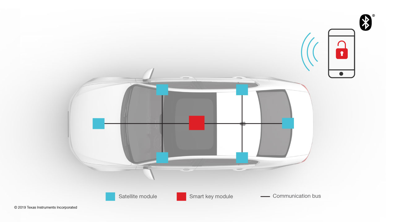
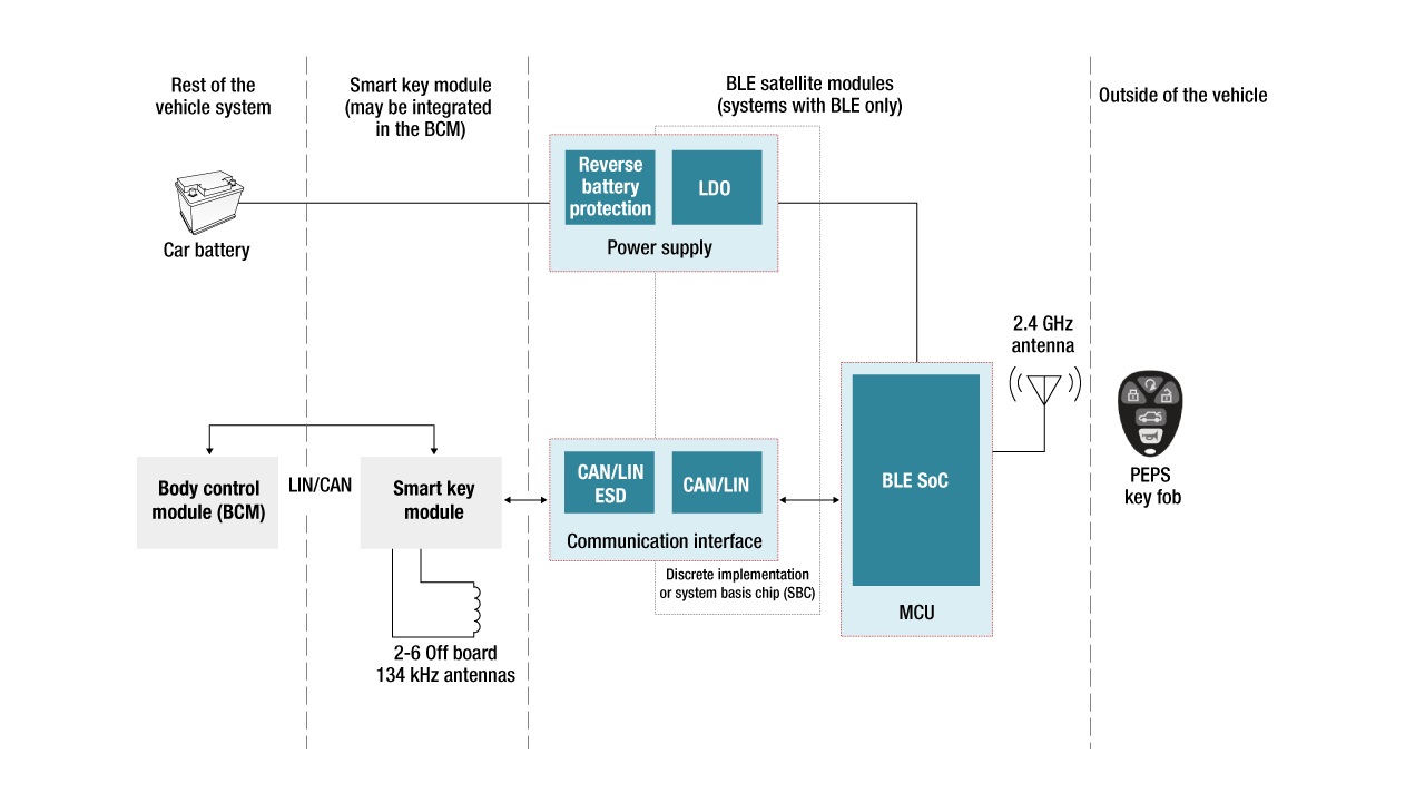
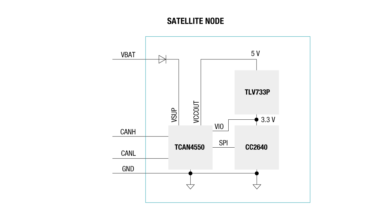
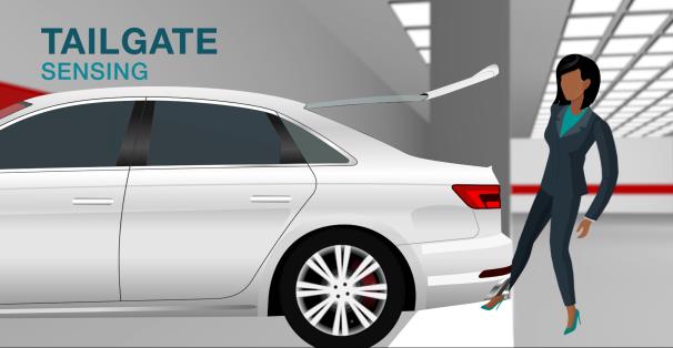
 The challenge is providing the next-generation functionality drivers expect with safer driver interaction. 

 In the white paper, Designing infotainment systems that are interactive, not distractive, I discuss ways design automotive systems that enhance the driver’s ability to drive safely while enjoying the ride.

Protector, monitor or gauge – selecting the correct battery electronics for your Li-ion-powered system

$
0
0

Lithium-ion batteries have high energy density and a long cycle life; they also lack the memory effect of other technologies. Such characteristics make them attractive for portable electronic systems. But lithium-ion batteries also need to operate within specified limits to be used safely, so batteries require electronics designed to respond or provide a signal to the system if the limits are exceeded.

Battery electronics monitor multiple conditions such as voltage, current and temperature and how they change over time. They need to sense the required combination of these parameters in order to respond, whether that’s sending a signal to the system, activating a switch to prevent charge or discharge, or opening a fuse. Figure 1 below shows an example of how the battery electronics might be configured in a typical battery pack.


Figure 1: Battery electronics within a battery pack

The type of battery electronics varies depending on the type of battery pack. Simple packs may need only a simple protector, ranging from a basic overvoltage protector to a more advanced protector that responds to under-voltage, temperature faults or current faults. Protectors can also operate as a secondary device along with a monitor or battery gauge.

Many advanced battery packs used in higher-cell-count batteries require a battery monitor. A battery monitor measures individual cell voltages, battery current and temperature, and reports these values to a gauge or microcontroller. The system uses this information to adjust performance accordingly; for example, by reducing the operating current if the temperature is too high. Battery monitors may provide a cell-balancing feature to extend battery run times as well as battery lifetimes. Monitors can also include protections available in integrated circuits (ICs), but with much higher configurability.

A gauge IC integrates the features of a battery monitor with a controller to provide advanced gauging algorithms. Gauge ICs report the remaining battery capacity, run time and state of charge. Software-based algorithms can enhance protections even further. Gauges often include other useful features such as a black-box function that helps diagnose battery packs that failed in the field, lifetime data logging of minimum and maximum parameter conditions, dynamic charger control, or authentication for secure batteries.

Figure 2 below outlines some of the key feature differences between the different types of battery electronics.

Figure 2: Feature differences between protectors, monitors and gauges

What features are most critical in choosing the optimal battery electronics for your system?

When evaluating the pros and cons of each battery electronics option, it’s important to consider the following characteristics of each:

  • Protectors offer the lowest complexity for simple pack designs.
  • Monitors offer the highest flexibility. You can write code specific to your system needs, which is often important when those needs are unique.
  • Gauge ICs offer the highest level of integration. They offer high-accuracy state-of-charge information and faster development time – since firmware is included – but might limit flexibility.

Figure 3 shows an example solution using the BQ769x0 battery monitor. The family includes devices for five- (BQ76920), 10- (BQ76930) and 15-cell (BQ76940) batteries. You can use the same controller software for any of the devices in the family, enabling flexibility for systems to go from three to 15 cells in series. The monitor continuously measures cell voltages, temperature and current through the sense resistor and reports this information to the microcontroller. It provides multiple configurable hardware protections and will open charge and discharge field-effect transistors (FETs) as needed to respond to fault conditions. The microcontroller can make decisions based on the information provided by the monitor – it can also enable/disable the FETs; control the cell-balancing feature; and even perform some basic gas gauging based on voltage, current and temperature information.


Figure 3: Example battery monitor solution featuring the BQ769x0 with a microcontroller

Figure 4 is an example of a slightly more advanced battery pack. Here, you see the same monitor family working with the BQ78350-R1 companion controller. The BQ78350-R1 comes equipped with firmware designed to work directly with the BQ7620, the BQ76930 or the BQ76940 digital monitor, helping accelerate product development. The BQ78350-R1 also performs fuel gauging and state-of-health reporting and includes many other features commonly included in TI fuel gauges, such as lifetime data logging and black-box recording.

Figure 4: Advanced battery pack featuring the BQ769x0, BQ78350-R1 controller with fuel gauge, BQ76200 high-side FET driver and BQ7718 secondary protector

Many systems require the redundancy of a secondary protector for overvoltage. This example features the BQ7718 stackable overvoltage protector, which can directly open a fuse if the primary protector fails.

Some systems may require the use of high-side FETs. High-side FETs enable continuous communication to the pack regardless of whether they are on or off. This means that the system can read critical pack parameters despite safety faults, and access pack conditions before allowing operations to resume. The BQ76200 high-side N-channel FET driver works well with the BQ76920, BQ76930 and BQ76940 monitors in systems needing high-side FETs.

There are many things to consider when designing systems with Lithium Ion batteries for safety and battery performance. Depending on the system needs, the appropriate protector, battery monitor or gauge can be selected.

Additional resources

Paving the way with ultrasonic sensing

$
0
0

Imagine a commute to work where, with the press of a button, your electric car automatically drives up to you, opens its door to let you in, navigates on its own through traffic to find the quickest route, pulls up to a garage with automatic gates, parks itself in an available spot, drops you off and charges itself on its own while parked. With the advancement of electric self-driving cars, this future is already starting to become a reality.

Sensors are at the heart of automation – embedded not only within vehicles to make smart driving decisions, but also in the surrounding environment to create a network of intelligence. With an interconnected system of sensors and data mapping the world as we see it, the road to innovation is truly limitless.

Video: how ultrasonic technology performs five unique tasks to improve the driving experience

(Please visit the site to view this video)

Ultrasonic sensors use sound waves to detect the presence or proximity of an object. This is done by transmitting a sound wave in the ultrasonic frequency band and listening for the return echo, which would be the result of the sound wave bouncing off an object in range. Time of flight describes the round-trip time it takes for a transmitted sound wave to come back to the receiver after bouncing off an object. Equation 1 is a simple formula that calculates the distance of an object from the ultrasonic sensor:

 Equation 1

Although many technologies can detect presence, proximity and position, ultrasonic is a popular choice because of its low system cost, performance in dirty environments, and ability to detect glass surfaces and perform in all lighting conditions.

Let’s explore how ultrasonic technology performs five tasks in and around the vehicle to improve the driving experience.

1. Garage gate sensing.

Gate sensors are implemented in garages, parking lots and other facilities for ticketing and security purposes. Ultrasonic sensors are beneficial here for their ability to operate indoors, outdoors and in any lighting condition. Ultrasonic technology makes it easy to detect larger objects like cars and motorcycles and dismiss smaller objects like animals and debris, therefore reducing the rate of false positives presented by other presence-sensing technologies.

2. Parking spot sensing.

Larger garages are adopting parking spot sensors to indicate whether a parking spot is empty or occupied. These sensors send information to a central server, which aggregates the number of empty and occupied spots in a certain area or floor of a garage and displays this information in external displays to help guide drivers to open parking spots. Sensors can be mounted on the floor or ceiling, but are typically mounted on the ceiling for easy installation in existing facilities. To conserve power, sensors can be duty-cycled and sampled once every few minutes to maintain a pretty accurate count.

3. Park assist.

In the past, ultrasonic park assist sensors were employed only in higher-end vehicles, helping drivers understand their surroundings by detecting obstructions. With the cost of ultrasonic sensors decreasing and their functional capabilities increasing, they are becoming more prevalent in lower- and mid-end vehicles as well. As the push towards autonomy progresses, employing ultrasonic park assist sensors in conjunction with other sensors will aid in the automated parking of vehicles. Industry standards require that ultrasonic park assist sensors sense at a range of up to 5 m and detect objects as narrow as a 75-mm wide.

4. Wireless charging pads/electric vehicle charging stations.

As electric vehicles become more common, so are charging stations. They typically come in one of two topologies: a wireless charging pad or a station that’s similar to a traditional gas station. Wireless charging pads are typically mounted on the floor of a parking spot, waiting for a car to drive up over it. Ultrasonic sensors ensure that the charging pad is fully covered under the vehicle to ensure best-case efficiency when charging. An embedded sensor can also ensure that there are no unintentional objects in proximity (such as a pet) before charging initiates. Wireless charging stations often have sensors on them as a measure to conserve electricity by keeping the station in sleep mode until it detects a car in proximity.

5. Kick-to-open trunks.

Kick-to-open trunks or smart trunk openers are becoming more prominent in vehicles. They enable hands-free opening of the trunk by hovering a foot below the bumper. Other body sensors located around doors and trunks can make sure that there is enough space to open and close them without hitting a wall, pole, another vehicle or a human. Capacitive sensing is used in these applications, but due to sensor failures in icy or snowy conditions, ultrasonic sensing is preferable, as such environments don’t affect its performance.

Get started with TI’s ultrasonic technology

Figure 1 below is a screenshot from the PGA460-Q1 ultrasonic sensor signal conditioning evaluation module with transducers, which helps you evaluate the performance of TI’s ultrasonic sensing IC in detecting obstructions and calculating Time-of-Flight. The figure shows the echo output (the yellow line) and time-varying gain and threshold registers (the white and blue lines). The built-in threshold registers make it easy for many of these applications to decide when to perform a function. For example, in the parking spot sensing example, it’s possible to set the threshold to ignore objects like a small animal but still detect desired objects like vehicles, which produce a stronger signal.

Figure 1: PGA460 ultrasonic GUI

Ultrasonic sensing is a beneficial technology for proximity and obstruction detection. It allows for intelligent decision making in vehicles, enabling them to sense the world around them to automate processes, improve efficiency and enhance safety.

Additional resources:


How to manage coefficient of thermal expansion in automotive designs

$
0
0

Coefficient of thermal expansion (CTE) is a way of describing how an object, material or liquid changes size with temperature. It’s measured by calculating the percentage change in length of a material per degree change of temperature.

When heated, the molecules of a substance begin to vibrate and move away from each other, causing expansion; removing heat creates the opposite process. While all materials expand with temperature, they do so at different rates. This difference is fundamental in understanding mechanical designs when it comes to short- and long-term reliability.

The principles of CTE apply in various industries; they are perhaps most common in construction. Figure 1 illustrates gaps in construction material that allow for expansion and reduce the pressure that various materials exert on each other.

Saw tooth bridge expansion joint

Figure 1: Expansion joint on a bridge in order to prevent cracking

CTE in automotive designs

Cars are especially susceptible to CTE, since they have to endure rapid changes in temperature in a short amount of time while withstanding high levels of vibration. Automotive designers need to consider various scenarios, from cold starting the system in temperatures as low as -40°C to rapid increases of temperature exceeding 100°C, or from starting at temperatures above 100°C and then cooling rapidly. These quick temperature changes cause the expansion and contraction of liquids and materials in the automobile, which applies stress on other materials and connections.

The greater the difference in CTE, the worse the problem, especially for materials that connect directly together. Electronic components are becoming an integral part of vehicle operation, from the electronic ignition to the sensors in the exhaust to the automatic safety systems. The reliability of these systems – both in the short and long term – is critical for a safe and proper operation.

It’s all in the package

When it comes to electronics, one of the most common CTE issues occurs around the solder joints –connections of electronic components to the printed circuit board (PCB). These joints experience pressure from both heat expansion and vibration. One way to overcome or at least minimize these issues is to choose the right electronic packaging.

While modern electronics have pushed for the integration of more components into smaller spaces to make designs more compact (and in doing so, increased the demand for leadless packaging), the removal of the legs (or leads) on the package increases its overall CTE. On a leaded package such as a thin-shrink small outline package, the legs form into a shape that act like a spring and are separated from the molding of the package. This means the package CTE more closely matches a typical PCB CTE, as illustrated in Figure 2. Less stress is applied to the solder connections due to small difference in the expansion and contraction.

Typical leaded package CTE vs typical PCB cte

Figure 2: Typical leaded package CTE vs. typical PCB CTE                

Although the footprint of a component is bigger because of the legs, often this means a larger die attached pad (DAP) is possible. A larger DAP helps manage thermals that cause expansion, also improving the thermal footprint size and amount of copper that is need to dissipate the heat generated by a power supply, for example..

When considering DC/DC converters, if you optimize the architecture of the integrated circuit to support higher-frequency operation and a better phase margin, you can reduce the number of external components to compensate for the area taken by the legs. In most cases, the package is much smaller than the inductor or capacitor when combined as a total solution size. Thus, it is possible to offer the highest levels of size reduction without compromising reliability and quality simply by designing the integrated circuit to reduce the overall bill of materials and number of external passives. An example of this is TI’s LM63625-Q1, developed specifically to minimize solution size without compromising the issues of CTE and vibration in the harsh environments of automotive systems.

With the right combination of circuit design and packaging, it is possible to manage various design challenges to create automobiles that people desire and that will remain reliable for many years.

The Spirit of Caring: TI honored for support of United Way of Metropolitan Dallas

$
0
0

(Please visit the site to view this video)

The United Way of Metropolitan Dallas touches the lives of one in five North Texans, and our company was recently recognized for playing a key role for ongoing support of the important work accomplished by the organization. The 2018-19 United Way campaign - which was led by our company's chairman, president and CEO, Rich Templeton, and his wife, Mary - raised more than $61.5 million.

“Philanthropy is alive and well in North Texas,” said Jennifer Sampson, McDermott-Templeton president and CEO of the organization. “Together, we have put opportunity in the hands of over 1 million North Texans. TI has been a pivotal and monumental supporter of United Way of Metropolitan Dallas since its inception almost 100 years ago. … TI’s annual contributions to United Way of Metropolitan Dallas and to our impact work are unparalleled.”

The United Way's annual campaign raises money to fund programs in education, income and health. Nearly 3,000 employees volunteered for more than 75 United Way projects. Our company’s employee engagement manager, Terri Grosh, received the individual volunteer award for inspiring thousands of TI employees to give their time and skills in our communities.

Real-time controllers get new connectivity capabilities

$
0
0
In the current industrial landscape, there are multiple solutions and architectures available for a wide variety of motor drive, factory automation and high-power grid applications. Many of these offer solid performance and connectivity but at a price...(read more)

New ways to design and implement user interfaces in dishwashers

$
0
0

Dishwasher products have evolved from a luxury appliance into an essential kitchen appliance for most households. While dishwasher prices vary mainly because of their capacity and brand name, there are now additional features like stainless-steel finishes and capacitive touch interfaces.


Capacitive touch technology is changing how consumers operate dishwashers, and also motivating designers to innovate. Let’s look at how capacitive touch technology offers new ways to design and implement user interfaces and address the associated challenges.


Capacitive touch through metal

Many dishwashers have a metal finish, which looks both elegant and robust. Implementing human machine interfaces on metal surfaces is challenging, however, because it requires machining and cutting a hole to accommodate mechanical buttons. In addition to compromising design elegance, mechanical buttons are also prone to failure in moist, dusty or dirty conditions. Capacitive touch through metal enables touch designs that are waterproof, dust-proof, wear-resistant and highly immune to noise. Consumers have the flexibility to operate the dishwasher while wearing gloves, and the technology can detect both soft and hard touches.


Unlike the traditional capacitive touch approach, MSP430™ microcontrollers (MCUs) with CapTIvate™ technology use an alternate approach for touch-through-metal applications (see Figure 1). The stack up includes a printed circuit board (PCB) with traditional capacitive touch sensors and a spacer topped with a grounded metal overlay. This mechanical structure forms a variable capacitor that generates changes in value when consumers apply force to buttons, sliders or wheels. The integrated CapTIvate peripheral on MSP430 MCUs is sensitive enough to detect metal-plate deflections at the micron level.


 Figure 1: Stackup of Metal Touch


Temperature and humidity drift

Most modern dishwasher products have steam and dry features that could introduce temperature and humidity drift into the system. Capacitive sensing measurement results will also drift over time in response to environmental changes such as temperature and humidity. A change in temperature, humidity or both can appear to the system as a touch if not properly interpreted.


To ensure reliable operation, the CapTIvate software library handles slow drift in a sensor’s measurement result caused by temperature or humidity in three ways:


  • The long-term-average (LTA) tracks measurement drift associated with gradual environmental changes through a slow-moving infinite impulse response filter.

  • The touch threshold varies proportionally with the LTA rather than as an absolute offset in order to maintain sensitivity.

  • If runtime recalibration is enabled, the system will recalibrate if the LTA drifts outside of a window set above or below one-eighth of the specified conversion count, renormalizing the sensors to the specified conversion count.


These three methods work together to ensure that the system behaves as designed across its lifetime, even with temperature and humidity changes.


More than a capacitive touch controller

Selecting a suitable MCU for a dishwasher user interface design is also critical because it could significantly shorten product development time, reduce overall system cost and save PCB space.


A suitable capacitive touch controller can manage many system functions in a dishwasher design: managing the backlight LED driver for the output user interface, communicating with other sensors in the system and monitoring the system status as well as providing self-diagnostics.


Figure 2: CapTIvate MCU Portfolio


Integrating all of these features with a single MCU requires more than a fixed-function or stand-alone capacitive touch controller. The MSP430 CapTIvate MCU family offers a wide portfolio of capacitive touch controllers (see Figure 2) that scale with your system integration requirements.


Additional resources


VIDEO: Bluetooth-enabled skin temperature patch demo

$
0
0

In this Connect series demo, Brandon shows us how to use our new high-precision digital temperature sensor, TMP117, in a SimpleLink™ Bluetooth-enabled skin temperature patch. Check it out!

The TMP117 provides a 16-bit temperature result with:

  • resolution of 0.0078°C 
  • accuracy of up to ±0.1°C across the temperature range of -20°C to 50°C with no calibration

(Please visit the site to view this video)

Additional resources:

Get the TI Design (reference design).

Learn more about the TMP117.

Check out SimpleLink Bluetooth wireless MCUs.

Subscribe to Connect, our weekly series.

Tweet @sensortocloud with future topic ideas!

Taking a modular approach to high-precision, high-current battery test equipment

$
0
0
The demand for lithium-ion (Li-ion) batteries has increased rapidly over the past few years, and that demand does not appear to be slowing down anytime soon. Booming industries like electric vehicles and grid infrastructure are leading the way in Li-ion...(read more)

Minimizing input power protection for smart speakers and smart displays

$
0
0

Smart speakers continue to enhance our homes with cutting-edge voice-recognition artificial intelligence and premium sound quality. When paired with other home automation devices – such as video doorbells, lighting systems, thermostats and security systems – smart speakers and smart displays are fast becoming the control hub for a smart home network.

To keep up with the growing market and stay ahead of the curve, designers are looking to reduce the size and heat dissipation of smart speakers while adding functionality and improving performance. Semiconductor devices that efficiently deliver higher performance in smaller packages become crucial to minimizing board space in space-constrained applications.

The majority of a circuit board comprises key components that directly influence the user experience, such as the audio system on chip, human interface controller for capacitive touch with haptic feedback, and LED driver engines and Class-D audio amplifiers. Other components in a smart speaker system such as power management perform essential tasks that do not directly impact the user experience, but do impact size and cost. It is possible to minimize these components for size while still maximizing performance.

One specific component is the input power-supply protection circuit, shown in Figure 1. Input protection, though sometimes taken for granted in many devices, is a critical circuit in the smart speaker to prevent damage to the entire system during power up or when connected to unreliable power supplies. Smart speakers are powered from either an external AC/DC wall adapter or an internal switched-mode power supply. This circuitry protects any downstream devices from being damaged in the event of a fault condition.

Figure 1: A reference block diagram showcasing the typical functions that make up a smart speaker

The primary concern on the input supply is an unnaturally high voltage or current event. TI has both integrated and discrete solutions to handle overcurrent protection (OCP) and overvoltage protection (OVP).

eFuse devices often handle OCP and OVP, integrating a power metal-oxide semiconductor field-effect transistor to disconnect all downstream circuitry under these fault events. eFuse devices also manage inrush current during startup, ensuring that system voltage increases in a controlled manner. Devices such as the TI TPS2595 offer this protection up to 18 V/4 A in a 2-mm-by-2-mm package.

For OCP, a common discrete implementation involves a current-sense amplifier such as the INA185 to measure the current across a shunt resistor. The output of the INA185 either feeds into an analog-to-digital converter (ADC) to digitize the value for a measurement, or into a comparator to provide an instant alert to the microcontroller. The ADC path offers a precise measurement of the current flowing in the system, but adds delay in reading the measurement due to the sampling frequency of the ADC. The comparator path is about 1,000 times faster (while consuming less power) but only provides a digital output signaling overcurrent, not the actual value of the current.

The ADC method works for systems that need to precisely measure current in a system and have the flexibility to change limits dynamically. The INA185 offers better than ±0.2% full-scale accuracy and is the industry’s smallest current-sense amplifier in a leaded package. Measuring only 1.6 mm by 1.6 mm, the device is a great fit for space-constrained systems that require an optimized board layout.


Enhance the design of your smart speakers and docking stations


Learn more in our circuit about fast-response overcurrent event detection in smart speakers and docking stations.

In smart displays, however, the system voltages are above 18 V, and thus need a faster OCP alert. An integrated eFuse device may not be able to operate in such a system, but the combination of a current-sense amplifier and a comparator can offer the same functionality with increased flexibility while taking up minimal board space. Nanosecond-delay comparators like TI’s TLV4041 consume only 2 µA of supply current and can be powered off a simple Zener diode. When paired, the combined solution of the INA185 and TLV4041 measures 5 mm2 and delivers response times up to 50 times faster than competitive devices.

Using an amplifier like the INA185 with a fast comparator provides a quick and precise OCP alert when the system current exceeds a custom-set threshold. Depending on the system, this limit can be set anywhere from milliamps up to a few amps. The TLV4041 also has a precision (1% over temperature) integrated reference to provide an accurate alert regardless of the current level, all in a 0.73-mm-by-0.73-mm footprint.

The discrete solution shown in Figure 3 saves board space by eliminating the need for an additional on-board regulator, and also works in both low- and high-voltage smart speaker systems. The same circuit works across different speaker models of varying supply voltage levels to further simplify your input power protection designs.

Figure 3: Functional circuit showing how to set up the INA185 and TLV4041 to generate an OCP alert signal for high-voltage systems

The combined solution of INA185 (2.56mm2) and TLV4041 (0.533mm^2) take up approximately 5mm^2 of board space after including the necessary passive components. This total solution size is 15% smaller than comparable integrated devices that offer current sensing functionality. Moreover, TLV4041 has a delay of just 450ns, which makes TI’s combined solution considerably faster than those that integrate a general purpose comparator alongside a current sense amplifier.

The combined solution of INA185 (2.56mm2) and TLV4041 (0.533mm2) take up approximately 5mm2 of board space after including the necessary passive components. This total solution size is 15% smaller than comparable integrated devices that offer current sensing functionality. Moreover, TLV4041 has a delay of just 450ns, which makes TI’s combined solution considerably faster than those that integrate a general purpose comparator alongside a current sense amplifier.

TI’s broad portfolio covers multiple solutions to minimize input power protection in smart speakers. Whether it is low-voltage speakers requiring an integrated device or high-voltage speakers that could use a discrete implementation, TI provides small-size solutions without compromising performance.

Additional resources

  • This Application Brief discusses the trade-offs of using an amplifier and comparator for power-supply protection in further detail.

Use fast, precise overcurrent detection to enable diagnostics in automotive safety systems

$
0
0

The electrification of vehicles is occurring not only in powertrain systems such as traction inverters, battery management and electric power steering, but also in automotive safety systems such as anti-lock brake systems or automated driving. Knowing that these systems are operating within the correct operational guidelines will be vital to helping ensure vehicle safety. Accurate measurement of current and a fast fault response time are critical to enabling debugging and diagnostics in these systems.

Figure 1 shows a typical overcurrent circuit consisting of a discrete operational amplifier and a discrete comparator.


Figure 1: Overcurrent detection implementation featuring a discrete operational amplifier and comparator

Several sources will determine the accuracy and response time of this system, including:

  • Shunt resistor (RS) tolerance and drift.
  • Amplifier circuit gain error (RI and RF).
  • Voltage divider (R1 and R2) error between the amplifier and comparator.
  • Comparator reference (R3 and R4) input error.
  • The amplifier circuit’s response time.
  • The comparator’s response time.

The errors caused by the shunt, gain and divider between the amplifier and comparator all contribute to a worst-case current measurement error. Depending on this error level, you will have to build margin into your design to ensure that it does not exceed the required operating parameters.


Design more efficient and reliable systems


Learn in our white paper how overcurrent protection enables longer lifecycles.

The total fault condition response time includes not only the amplifier and comparator response times; you must also take into account microcontroller (MCU) cycle time as well as the protection circuit’s turn-on and turn-off times. The total response time must be less than what is required to bring the system to a safe operating condition. Typically, the MCU cycle time and protection circuit are fixed; therefore, you’ll have to adjust the amplifier and comparator response times to meet the system requirements. TI offers a wide range of solutions with various response times for amplifiers and comparators.

If you want to improve the current-sensing accuracy, using higher-precision lower-drift resistors with the circuit shown in Figure 1 is one option; however, as the accuracy and drift of the external components increases, so does the cost. An alternative is to use a current-sense amplifier such as the TI INA185. Current-sense amplifiers integrate a precision matched-resistor gain network that cost-effectively reduces the gain error as well as the drift. In the case of the INA185, the gain error is ±0.25% with 8 ppm/°C drift, or ±0.33% over temperature.

It is also possible to improve the reference error by using better resistors. Using a comparator with an integrated precision reference such as the TI TLV4021 can also offer significant improvement, with ±0.04% error over temperature. Figure 2 shows a circuit that uses both the INA185 and TLV4021 for an overcurrent detection circuit.

Figure 2: Overcurrent detection implementation featuring a precision current-sense amplifier and precision comparator

This leaves divider error as the primary error source. You can eliminate this error source by using a current-sense amplifier such as the TI INA301, which integrates the comparator and a precision reference, as shown in Figure 3.

 
Figure 3: INA301 functional block diagram

The INA301 has a precision current source on-chip that requires only a single external resistor to set the threshold. In addition, the total response time for the alert output is less than 1 µs.

Monitoring a system’s current provides a leading indicator of potential issues. Increasing the accuracy of your overcurrent detection implementation can improve system power efficiency by minimizing the allocated headroom. There are many overcurrent detection solutions that can be optimized based on the key concerns of a particular application: cost, solution size, accuracy, or response time. You can trade off the low cost of typical discrete implementations with the increased precision offered by current-sense amplifiers and comparators with integrated references.

References

  1. Download the INA185 data sheet.
  2. Download the TLV4021 data sheet.
  3. Download the INA301 data sheet.
  4. Getting Started with Current Sense Amplifiers, Texas Instruments Training Series

Designing compact, efficient and high performing multiparameter patient monitors

$
0
0
Continuous measurement of patient vital signs like heart rate, respiration rate and blood oxygen saturation (SpO2) is crucial for effective care, and the ability to measure those simultaneously makes multiparameter patient monitors increasingly important...(read more)
Viewing all 4543 articles
Browse latest View live


<script src="https://jsc.adskeeper.com/r/s/rssing.com.1596347.js" async> </script>