Quantcast
Channel: TI E2E support forums
Viewing all 4543 articles
Browse latest View live

New metering technology makes every drop count

$
0
0

Every drop counts

The statistics are alarming: In the United States alone, household leaks waste about 900 billion gallons of water each year. To put that number in perspective, that’s enough water to supply about 11 million homes annually.1 And other countries – from Europe to Asia – face similar challenges. Compounding this problem are anticipated water shortages.2

But help is here. Ultrasonic technology gives water meters installed in smart buildings and smart cities the ability to detect and localize leaks as small as one drop every few seconds. Cities from Austin to Antwerp are installing high-tech smart water meters that give customers the information they need to find leaks and conserve water while helping utilities identify infrastructure leaks in aging pipes and broken water mains.

Every drop counts

“The water we have today is the only water we will ever have,” says Holly Holt-Torres, water conservation manager for the City of Dallas Water Utilities. “We have to conserve it. Technology will allow us to do that at an increasingly higher level.”

But this ultrasonic technology has applications that extend beyond water meters. The same technology can be used in meters that measure natural gas flow and even detect the mixture of gas flowing through pipes. It can even help medical professionals regulate oxygen delivery in surgical equipment.


 Learn more about our ultrasonic sensing MSP430™ microcontrollers.

Going with the flow

Ultrasonic waves, of course, are not new. Bats, for example, use ultrasonic ranging to avoid obstacles and catch insects at night. And in more high-tech applications, it is used in material discernment, collision avoidance in automobiles, and industrial and medical imaging.

Now it’s being used in water meters and other flow meters. Meters traditionally have relied on an electromechanical system with a turning spindle or gear that uses a magnetic element to generate pulses. But – as is the case with thermostats, motors and lots of other everyday devices – electromechanical systems in flow meters are rapidly transitioning to electronic systems.

In these systems, a pair of immersive ultrasonic transducers measures the velocity of acoustic waves in the fluid. The velocity of acoustic wave propagation is a function of the viscosity, flow rate and direction of the fluid flowing through the pipe. Ultrasonic waves travel at different speeds depending on the stiffness of the media they’re traveling through.

The accuracy of the measurement depends on the quality of the transducer, precision analog circuitry and signal processing algorithms. Acoustic or ultrasonic transducers are piezo materials that convert electric signals to mechanical vibrations at a relatively high frequency of hundreds of kilohertz. Typically, a pair of ultrasonic transducers in the range of 1-2 MHz must be well-matched and calibrated in order to measure flow accurately. They make up a significant part of the flow meter’s cost. The sensor system must operate at very low power to ensure a 15-20 year battery life.

Our company’s advanced flow metering chip, the MSP430FR6043, includes a unique analog front end and algorithm, which significantly improves accuracy while reducing overall cost and power consumption. Our flow metering architecture leverages high-performance analog design, advanced algorithms and embedded processing to mitigate the need for an expensive pair of ultrasonic transducers. Analog front end and signal processing algorithms compensate for transducer mismatch.

Making every drop count
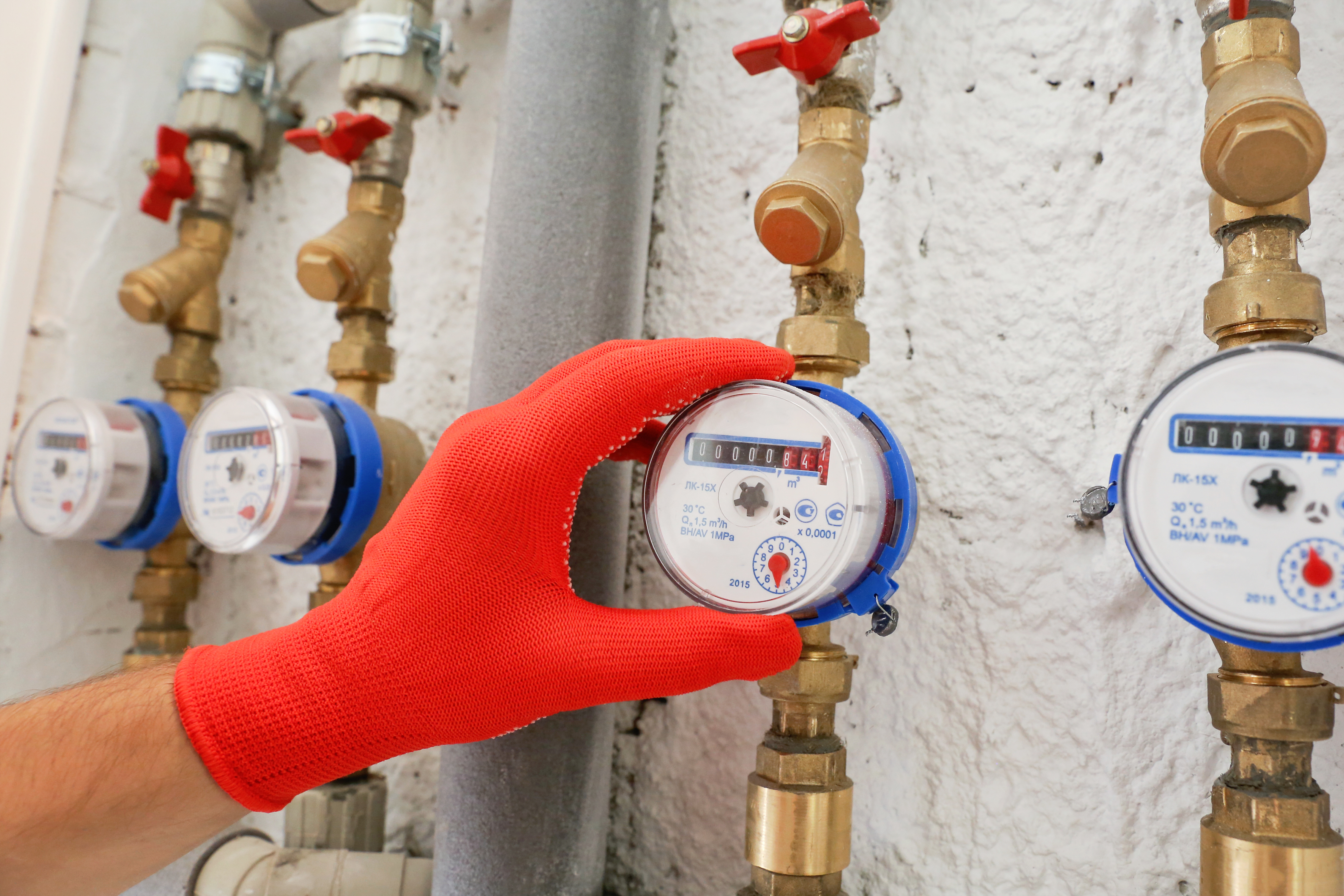
Water meterA typical ultrasonic flow meter transmits an ultrasonic wave and measures the differential delay at the receiver to estimate the rate of the flow. Delay measurements are usually handled by a time-to-digital-converter circuit that monitors the zero crossing of the received waveform. The challenge with the typical approach is that it is not sensitive enough to detect flow levels with high accuracy.

Our architecture deploys a smart analog front end featuring a high-performance analog-to-digital converter to improve signal-to-noise quality and overcome calibration inaccuracies. This approach has several benefits:  

  • It can achieve higher accuracy by reducing interference and improving signal-to-noise ratio.
  • The architecture can measure a wide dynamic range of flow, from a fire hose to a small leak.
  • By using a lower voltage driver, it significantly saves on power and cost. The average current for one measurement per second is less than 3 microamps. This translates to a battery life of more than 15 years.
  • It can detect turbulence, bubbles and other flow anomalies, which is important for flow analysis and servicing the pipelines.
  • The technology is robust to amplitude variations in the two directions of the flow, which may occur in water and gas at higher flow rates.

Many other TI technologies are critical for a high-performance flow meter. A low-power microcontroller with integrated ultrasonic analog front end, a high-performance clock reference, a low-quiescent current power management and ultra-accurate impedance matching of transmit driver and receive amplifier paths are examples of additional differentiating technologies in these flow meters.

Together, these technologies can help conserve one of our most precious resources.

Learn more about our ultrasonic sensing solution library for ultra-low-power flow metering devices.

Read our Corporate Citizenship Report to learn how our company is committed to conserving water and other resources.


1 Environmental Protection Agency

2 Earth’s Future: Adaptation to Future Water Shortages in the United States Caused by Population Growth and Climate Change.


How to reduce the size of your 13-W PoE PD solution

$
0
0

You just got a big product out the door and are enjoying some well-deserved downtime when your product manager decides to swing by. Surprise, surprise: he wants the next-generation product to have more features and a smaller form factor. Luckily, you may be able to squeeze out some area from your Power over Ethernet (PoE) powered device (PD) solution.

If you’re after power density, consider the following when choosing a new PoE PD controller:

  • Does it integrate a PoE PD front end and a DC/DC controller? Does it have an integrated PD field-effect transistor (FET) and an integrated switching FET? Higher integration will usually save board space and streamline the supply chain, since fewer components need to be purchased and planned for.  For a robust solution consider a 100-V PD FET and a 150-V switching FET.  This will provide margin against variation of the clamping voltage of the input TVS and the ringing of the switching node in the Flyback.  
  • Does the PoE PD controller offer primary side regulation (PSR)? PSR is a crucial feature that will enable you to remove the optocoupler and shunt reference, along with the diodes and resistor capacitors used for soft start.
  • Does it offer spread-spectrum frequency dithering (SSFD)? This feature reduces electromagnetic interference (EMI) by spreading the noise in a broader frequency band.  SSFD typically results in a reduction of 4-6 dB at the fundamental switching frequency and 10-20 dB for higher-frequency harmonics, enabling a ~2x reduction in the high-voltage common-mode capacitors, which are usually big and expensive.
  • Does the PoE PD controller operate in continuous conduction mode (CCM) or discontinuous conduction mode? CCM has lower peak currents, which enables you to use lower input and output capacitors and injects less noise, thus requiring smaller filtering components.
  • Does it feature advanced startup? This feature provides full current to the DC/DC controller during the soft-start phase before the auxiliary winding is fully up. Advanced startup allows you to reduce the VCC capacitor from ~22 µF to 1 µF, enabling the use of a ceramic capacitor, which is smaller and more reliable.

TI’s newly released TPS23755 is a Type 1 (limited to 13W of input power) PoE PD device that checks all of the above boxes.

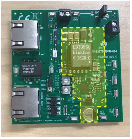
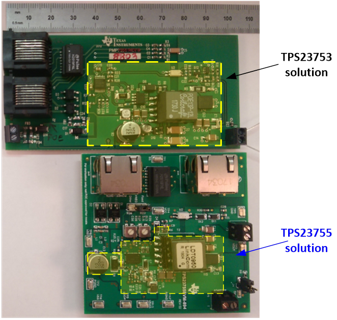
Figure 1 shows a visual comparison between a 12-V, 1-A solution for the TPS23753A vs. the new TPS23755 solution. Note that the figure does not include the EMI filter. The TPS23753A operates in CCM mode and integrates the PoE PD (integrated FET) with a DC/DC controller. The TPS23755 adds the integrated switching FET, PSR, advanced startup and SSFD.

Figure 1: Board Space comparison for TPS23755 vs. TPS23753

To appease your product manager and squeeze out some area from your PoE PD solution, consider evaluating TI’s TPS23755 evaluation module for IEEE 802.3at Type 1 PoE PD applications and “IEEE 802.3at Type-1 PoE and 12-V adapter input to point of load reference design for IP network camera” to get started with your Type 1 PoE design. For applications requiring 5V output consider evaluating TI’s TPS23758 evaluation module for IEEE 802.3at Type 1 PoE PD applications.

Additional resources

Two changes to Behind the Wheel

$
0
0

Thank you for reading Behind the Wheel. This week, we are refreshing the look and structure of technical blogs on E2E to simplify how you find and select content relevant to your interests. 

  • Moving forward, posts will be listed under the category of “technical articles” rather than “blogs.”
  • In addition, the name, Behind the Wheel will be replaced with the topic category of “automotive.” 

What is staying the same? You will continue to find quality content that shares automotive engineering expertise, industry insight and product knowledge. And existing content is still searchable on the TI E2E site and TI.com.

Stay tuned for our next article, coming soon!

Changes to Analog Wire

$
0
0

Thank you for following our company’s Analog Wire blog. This week, we are refreshing the look and structure of the technical blogs on the TI E2E site to simplify how to find and select the relevant content for your interests.

  • Moving forward, you will find the content under the category of “technical articles” rather than “blogs.”
  • In addition, the name will change from Analog Wire to Analog and you will see a new avatar using the image below.

What is staying the same? You will continue to find quality content that shares engineering expertise, industry insight and product knowledge. And existing content is still searchable on the TI E2E site and TI.com.

We invite you to continue following and watch for the next article, coming soon!

Thank you.

Changes to ConnecTIng Wirelessly coming soon...

$
0
0

Thank you for following our company’s ConnecTIng Wirelessly blog. This week, we are refreshing the look and structure of the technical blogs on the TI E2E site to simplify how to find and select the relevant content for your interests.


1) We are changing the content category name from “blog” to “technical articles.”


2) In addition, ConnecTIng Wirelessly is moving under the topic heading "embedded processing," and you will see a new avatar using the image below.


What is staying the same? You will continue to find quality content that shares engineering expertise, industry insight and product knowledge. And existing content is still searchable on the TI E2E site and TI.com.


We invite you to subscribe to the embedding processing articles and watch for the next one coming soon!

Thank you.


Changes to MSP Low-Power Plays coming soon...

$
0
0

Thank you for following our company’s MSP Low-Power Plays blog. This week, we are refreshing the look and structure of the technical blogs on the TI E2E site to simplify how to find and select the relevant content for your interests.


1) We are changing the content category name from “blog” to “technical articles.”


2) In addition, MSP Low-Power Plays is moving under the topic heading "embedded processing," and you will see a new avatar using the image below.


What is staying the same? You will continue to find quality content that shares engineering expertise, industry insight and product knowledge. And existing content is still searchable on the TI E2E site and TI.com.


We invite you to subscribe to the embedding processing articles and watch for the next one coming soon!

Thank you.

Changes to Power House

$
0
0

Thank you for following our company’s Power House blog. This week, we are refreshing the look and structure of the technical blogs on the TI E2E site to simplify how to find and select the relevant content for your interests.

Moving forward, you will find the content under the category of “technical articles” rather than “blogs.” In addition, the name will change from Power House to the topic category of Power management and you will see a new avatar using the image below.

What is staying the same? You will continue to find quality content that shares engineering expertise, industry insight and product knowledge. And existing content is still searchable on the TI E2E site and TI.com.

We invite you to continue following and watch for the next article, coming soon!

Thank you.

Changes to Industrial Strength coming soon...

$
0
0
Thank you for following our company’s Industrial Strength blog. This week, we are refreshing the look and structure of the technical blogs on the TI E2E site to simplify how to find and select the relevant content for your interests. This week,...(read more)

Changes to Motor Drive & Control coming soon...

$
0
0

Thank you for following our company’s Motor Drive & Control blog. This week, we are refreshing the look and structure of the technical blogs on the TI E2E site to simplify how to find and select the relevant content for your interests. This week, we are changing the content category name from “blog” to “technical articles.” In addition, Motor Drive & Control is moving under the topic heading 'industrial' and you will see a new avatar using the image below.


What is staying the same? You will continue to find quality content that shares engineering expertise, industry insight and product knowledge and existing content is still searchable on the TI E2E site and TI.com.

We invite you to subscribe to the industrial articles and watch for the next one coming soon!

Thank you.

Changes to The Process

$
0
0

Thank you for following our company’s The Process blog. This week, we are refreshing the look and structure of the technical blogs on the TI E2E site to simplify how to find and select the relevant content for your interests. This week, we are changing the content category name from “blog” to “technical articles.”

The Process is moving under the topic heading Embedded processing and you will see a new avatar using the image below.

 What is staying the same? You will continue to find quality content that shares engineering expertise, industry insight and product knowledge. And existing content is still searchable on the TI E2E site and TI.com.

We invite you to subscribe to the Embedded processing articles and watch for the next one coming soon!

Changes to Enlightened: The TI DLP Blog coming soon

$
0
0
Thank you for following Enlightened: The TI DLP Blog. This week, we are refreshing the look and structure of the technical blogs on the TI E2E site to simplify how to find and select the relevant content for your interests. Moving forward, you will find...(read more)

Overcoming Ethernet connectivity challenges on the power grid

$
0
0
Traditionally, the power grid consisted of stand-alone equipment working independently; maintenance was a manual process using paper-based inspection and reporting. As equipment like protection relays, circuit breakers and smart meters became digital...(read more)

Optimizing power density with eFuses

$
0
0

Do you still remember what it was like have dial-up internet? If not, here’s an audio snippet that may jog your memory! It was only a few years ago that you had to wait 10 minutes for someone to get off the phone before you could log in to your AOL Instant Messenger account, which probably took another five minutes with the typical 40-kbps transfer speeds. Now, even though we can download high-definition videos in seconds and have high-speed internet access in almost any developed area, we still want more data and faster bandwidth. And exciting innovations from data centers to semiconductors are delivering.

Increased bandwidth demands have made power density more important for electronic equipment like servers, routers and switches as circuit board space becomes more constrained. As a result, power integrated circuits (ICs) must pass more power (with a lower on-resistance [RON]) in a smaller footprint. Often this relationship between RON and footprint size is inversely related – optimizing one will worsen the other.

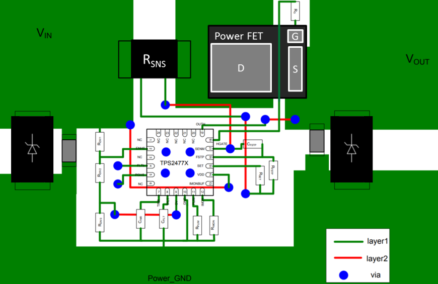
One subset of power ICs that has seen significant innovation in recent years is the hot-swap controller. Historically, external metal-oxide semiconductor field-effect transistor (MOSFET) hot-swap controllers have been a very popular power-path protection solution. However, the footprint for such a solution can be quite large given the need for an external sense resistor and power MOSFET. As shown in Figure 1, a hot-swap solution can take up a significant amount of board space.

Figure 1: An external MOSFET solution with the TPS2477x hot-swap controller

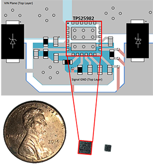
Decreasing the package size of these ICs will increase the RON, which will worsen the power performance. However, with TI’s proprietary processes, it is possible to optimize both parameters and achieve superior power density in a very small footprint. Figure 2 shows the TPS25982– a new 24-V, 15-A eFuse that comes in a 4-mm-by-4-mm package.

Figure 2: TPS25982 (center) and TPS2595 (right) size comparison

For even smaller footprint solutions, the TPS2595 eFuse comes in a 2mm x 2mm package and for higher voltages, the TPS1663 eFuse supports up to 60V, as shown below in Table 1.

Device

Voltage

Current

RON

Package

TPS25982

2.7 V-24 V

15 A

3 mΩ

4-mm-by-4-mm quad flat no-lead (QFN)

TPS2595

2.7 V-18 V

4 A

34 mΩ

2-mm-by-2mm QFN

TPS1663

4.5 V-60 V

6 A

31 mΩ

4-mm-by-4mm QFN

Table 1: Texas Instruments eFuse options

As overall power demands increase in the market, board space becomes more and more valuable. As a result, optimizing power efficient solutions in a small footprint will be something all power designers will have to consider. 

VIDEO: Wearable, wireless patient monitoring demo with Bluetooth 5

$
0
0

In this Connect series demo, we will demonstrate a new reference design available on ti.com for a simple, wearable multi-parameter patient monitor for synchronized electrocardiography (ECG) and photoplethysmography (PPG) measurements. Check it out!

The reference design features:

  • Raw data to calculate heart rate, SpO2, and PTT
  • Bluetooth 4.2 and 5.0 support
  • Battery life of 30 days using highly efficient DC/DC converters
  • Small form factor

(Please visit the site to view this video)

6 situations where small amplifiers solve big challenges in vacuum robots

$
0
0
After a busy week, cleaning is the last thing people want to do with their downtime. The vacuum robot, which has been around for about 23 years, is getting more intelligent and automatic, enabling consumers to focus on what’s really important. ...(read more)

Design, optimize and simulate an active filter within minutes

$
0
0

You are on a quest to design an active filter. You have the specifications of the filter’s frequency response, but how do you create a circuit that does just what you want?

If you took the conventional approach, you would need to manipulate the second-order control system equations by consulting multiple filter-response coefficient tables; plot and compare multiple filter responses; select the filter response that best meets your specification; choose a circuit topology and calculate the passive component values by solving complex quadratic equations; and pick standard, graded passive components and an operational amplifier (op amp) that closely match the calculated values. You’ll need to repeat component selection and calculations until you achieve the desired performance – a process that could easily take weeks, if not months.

TI’s Filter Design Tool streamlines the system design, circuit design and circuit verification process and helps you select a filter circuit that has high chance for first-pass success.


Designing a robust filter circuit, made easy

 Design, optimize and simulate complete multistage active filter solutions within minutes. Launch the tool now.

The Filter Type tab in the tool (Figure 1) gives you the option to select low-pass, high-pass, band-pass, band-stop (notch) or all-pass filters.

 Figure 1: Filter Type selection screen

Figure 1: Filter Type selection screen

Click one of the filter types to move forward to the Filter Response screen (Figure 2).

Figure 2: Filter Response screen

Figure 2: Filter Response screen

As you enter your design specifications on the left, the chart on the right updates the waveform to reflect the characteristics of your selected filter response. You can switch between magnitude, phase, group delay and step response by clicking the button above the chart.

The table beneath the waveform presents the filter responses that meet your design specifications. The first filter response is displayed by default, but you can check or uncheck multiple other filter responses to compare or hide their characteristics and performance.

To advance to the Topology screen (Figure 3), click Select to the right of the filter response you want.

Figure 3: Topology screen

Figure 3: Topology screen

The Filter Design Tool currently supports Sallen-Key and Multiple Feedback topologies for low-, high- and band-pass filters. Band-stop filters only supports Bainter topology because of the challenges in suppressing ringing within the stop-band region for Sallen-Key topology, and the difficulty in meeting the gain and natural frequency for the Multiple Feedback topology.

The Filter Design Tool recommends the best topology based on your filter specification and applies this circuit to all stages. You have the option to choose an alternate topology to meet your design priorities. Toggling the “Use same topology for all stages” switch gives you the ability to mix and match topologies, as shown in Figure 4.

Figure 4: Customize circuit topology for each stage

Figure 4: Customize circuit topology for each stage

You can observe the characteristics of each stage by clicking a particular row in the table, as shown in Figure 5. Advanced users could potentially rearrange the circuit sequence in the exported TINA-TI™ software schematic to meet their design priorities.

Figure 5: Evaluate characteristics of each stageEvaluate characteristics of each stage

Figure 5: Evaluate characteristics of each stage

The Design tab (Figure 6) lets you quickly complete three crucial design steps: schematic creation, op amp selection and component tolerance analysis.

Figure 6: Design screen

Figure 6: Design screen

The complete schematic with the actual amplifier and passive components is displayed on the Design screen. The tool uses the standard resistor and capacitor values that closely match the calculated values. It is always a design challenge to balance between performance and component cost.

The default power supply is ±5 V and can be easily updated on the top left window of the design screen. The gain bandwidth slider range is set to 10 to 200 times the calculated gain bandwidth. The left slider bar is set to the recommended 100 times the calculated gain bandwidth by default. You can lower the gain bandwidth margin by sliding it to the left, to the yellow and red region of the heat map.

It’s good practice to perform a simulation if you choose a lower gain-bandwidth amplifier. If you have a specific design priority such as low power, high precision or number of lanes, you can click Select Alternate Op Amp on the design screen. This brings you to a dedicated op-amp selection screen, as shown in Figure 7. On this screen, you will be able to specify your design priorities and pick the best TI op amp for your design. Click Select to pick your op amp or Cancel to return to the Design screen.

Figure 7: Select alternate amplifier

Figure 7: Select alternate amplifier

The default resistor and capacitor grades are set to ensure that the deviation between the actual and target values is less than 5% for gain, natural frequency and Q. You can trade off performance and accuracy by choosing a lower-grade capacitor and resistor for reduced costs. The tool will recalculate the actual gain, natural frequency and Q with your new selection. If any of the values deviate more than 5%, the circle of the last column on the table will turn from green to yellow. If the deviation is greater than 10%, the circuit will turn red on the design screen as shown in Figure 8.

The rule of thumb to achieving high accuracy and low cost is to lower the grade for the passive components and still keep the color of the circles green. If you must operate within yellow or red, export the design and run a thorough analysis to ensure that the design still meets your specifications.

 FFigure 8: Use merit as a quick performance indicatorigure 8: Use merit as a quick performance indicator

Figure 8: Use merit as a quick performance indicator

Once you have successfully created and analyzed your design, you can export the design information to a PDF report, and the schematic to TINA-TI software as shown in Figure 9. It’s also a good idea to perform a Spice simulation, as not all the op-amp characteristics have been included in the design considerations.

Figure 9: Export Screen

Figure 9: Export Screen

The new Filter Design Tool has a simple user interface powered by intelligent and computation-intensive algorithms. It drastically enhances your experience in designing a robust filter circuit from the first step to the last.

Imaging radar: one sensor to rule them all

$
0
0

There is still some confusion in the industry about the different roles that three major sensor types – camera, radar and LIDAR – have in a vehicle, and how each can solve the sensing needs of advanced driver assistance systems (ADAS) and autonomous driving.

Recently, I had an interesting discussion with one of my friends, who knows I work with TI millimeter-wave (mmWave) sensors for radar in ADAS systems and autonomous vehicles (AVs).

My friend doesn’t skip an opportunity to tease me any time he reads about how an autonomous vehicle performed in different driving situations, like obstacle detection. Here’s how one conversation went:

Matt: “If that car had LIDAR, it would have easily identified the object in the middle of the lane.”

Me: “As always, I disagree.”

Matt: “What?! Why would you disagree? There was a camera sensor and a radar sensor in that vehicle, and still the ADAS system totally missed the vehicle in the middle of the lane.”

Me: “When you read about these recent events, you’ll notice that the cameras are often exposed to glare or other elements that cause the camera to miss an object in the road. Cameras are sensitive to high-contrast light and poor visibility conditions, such as rain, fog and snow. In this case, the radar sensor probably did identify the target.”

Matt: “Still, we keep running into different situations thatthese ADAS and AV systems seem to find very challenging. What is missing?”

Me: “It seems the ADAS’ decision-making system relied on the camera as the primary sensor to decide if the target was really there, or whether it was a false alarm.”

Matt: “So the car’s radar and camera can’t be trusted. So you are left with LIDAR as the only reliable sensor. Isn’t that right?”

Me: “Not quite. LIDAR is not as sensitive to visibility conditions as the camera is, but it is sensitive to weather conditions like fog, rain and snow. In addition, LIDAR is still considered to be very expensive, which probably limits its usage initially to higher-end level 4 and 5 autonomous vehicles.”

Matt: “So we are doomed! There is no single sensor that can make autonomous vehicles truly reliable. We will always need all three, which means very expensive autonomous vehicles.”

Me: “You are partly right. Level 4 and 5 autonomous vehicles will probably need all the three sensors – camera, LIDAR and radar – to provide high reliability and a fully autonomous driving experience.

However, for more economic vehicles requiring partial autonomy at levels 2 and 3, where high-volume mass production has already started, imaging radar using TI mmWave sensors delivers the high performance and cost-effectiveness that can enable broad adoption of ADAS functionality.”

So what is imaging radar?

As I explained to Matt, imaging radar is a subset of radar that got its name due to the clear images that its high angular resolution is capable of providing.

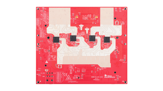
Imaging radar is enabled by a sensor configuration in which multiple low-power TI mmWave sensors are cascaded together and operate synchronously as one unit, with many receive and transmit channels to significantly enhance the angular resolution as well as the radar range performance. mmWave sensors, when cascaded together, can reach an extended range of up to 400 m using integrated phase shifters to create beamforming. Figure 1 shows the cascaded mmWave sensors with their antennas on an evaluation module.

 
Figure 1: An imaging radar evaluation module with four cascaded TI mmWave sensors

mmWave technology for imaging radar

The main reason why the typical radar sensor hadn’t been considered the primary sensor in vehicles until recently is its limited angular resolution performance.

Angular resolution is the ability to distinguish between objects within the same range and the same relative velocity.

A common use case that highlights the imaging radar sensor’s advantage is being able to identify static objects in high resolution. The typical mmWave sensor has a high velocity and range resolution, which enables it to easily identify and differentiate between moving objects, but it is quite limited when it comes to static objects.

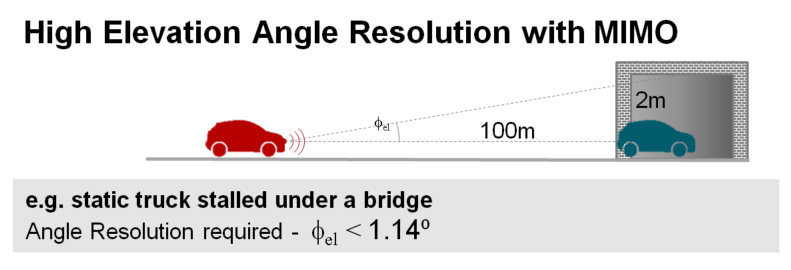
For example, in order for a sensor to “see” a stopped vehicle in the middle of the lane and distinguish it from light poles or a fence, the sensor requires a certain angle resolution in both the elevation and azimuth. .

Figure 2 shows a vehicle stuck in a tunnel with smoke coming out of it. The vehicle is approximately 100 m away and the tunnel height is 3 m.

Figure 2: The front radar of the approaching car needs a high-enough angle resolution to differentiate between the tunnel and the stopped vehicle. mmWave sensors can see through any visibility conditions, like smoke.

In order to identify the vehicle in the tunnel shown in Figure 2, the sensor needs to differentiate it from the tunnel ceiling and walls.

Achieving the scene classification requires these elevation and azimuth angle resolutions:

ɸ (elevation) = arctan (2 m/100 m) = 1.14 degrees

ɸ (azimuth) = arctan (3.5 m/100 m) = 2 degrees

Where 2 m is the tunnel height minus the vehicle height, 100 m is the distance between the approaching vehicle with imaging radar and the vehicle stopped in the tunnel and 3.5 m is the distance between the stopped vehicle and the tunnel walls. Figure 3 illustrates how mmWave sensors enable high angular resolution in order to “see” the vehicle.

Figure 3: How mmWave sensors achieve high elevation angular resolution with multiple-input multiple-output (MIMO) radar.

Relying on other optical sensors may be challenging in certain weather and visibility conditions.Smoke, fog, bad weather, and light and dark contrasts are challenging visibility conditions that can inhibit optical passive and active sensors such as cameras and LIDAR, which may potentially fail to identify a target. TI mmWave sensors, however, maintain robust performance despite challenging weather and visibility conditions.

Currently, the only sensor that keeps robustness in every weather and visibility condition, and that can achieve 1-degree angular resolution in both azimuth and elevation (and even lower with super-resolution algorithms) is the imaging radar sensor. 

Conclusion
Imaging radar using TI mmWave sensors provides great flexibility to sense and classify objects in the near field at a very high resolution, while simultaneously tracking targets in the far field up to 400 m away. This high-resolution and cost-effective imaging radar system can enable level 2 and 3 ADAS applications as well as high-end level 4 and 5 autonomous vehicles, and act as the primary sensor in the vehicle.

Additional resources

Do all rails need low Iq?

$
0
0

a smart meter

All designers of ultra-low power systems are concerned about battery life. How much time will elapse before the battery in a fitness tracker will need recharging? Or, for primary cell systems, how long will it be before a technician must service the smart meter and change the battery? Clearly, the design goal is maximum battery runtime. For a fitness tracker, a week of runtime may be good, but a smart meter operates for 20 years or more. What do you need to consider in each of the various subsystems to achieve this runtime?

In many systems, one or two voltage rails are always enabled. These power the system microcontroller (MCU), a critical sensor or maybe a communication bus. These always-on rails need to have very high efficiency to extend the battery runtime. A good subsystem design reduces the current drawn by each of the always-on subsystems to a minimum – many times this is less than 10 µA, or even 1 µA, total. As I discussed in this technical article, an ultra-low power supply is required to reap the benefits of these subsystem optimizations. In rails with very low current consumption, this translates to a power supply with ultra-low quiescent current (IQ), such as the 60 nA IQTPS62840.

You might be tempted to think that it’s most important to minimize the current consumption of each of the power supplies while they are running. Reducing the IQ increases efficiency and thus extends the battery runtime by consuming less battery power. But is the efficiency increase always significant? For systems that operate at relatively higher load currents, such as displays and some sensors, the answer is clearly no; the output power is much greater than the IQ power. For example, if the display in a fitness tracker draws 12 V at 5 mA (60mW total), the 100µA IQ drawn from the 3.6V battery (0.36 mW total) is insignificant.

More important for these types of subsystems is the power consumption when disabled. An ultra-low power system turns off power-hungry subsystems most of the time in order to conserve the battery. Thus, the shutdown current becomes critical to the system’s battery life. This leakage current, as it is frequently called, may be so high that you will have to add a load switch to disconnect the subsystem from its power source to further reduce its shutdown current. The TPS62748, high efficiency buck converter, provides both a load switch and 360 nA ultra-low IQ for such systems.

When a load switch is not used, you must consider both the leakage current into the device itself and its load if there is a path to the load through the device. This is frequently the case with a boost converter, so specific circuitry is sometimes added to break this path, such as the isolation switch in the TPS61046, boost converter. In other cases, this path is specifically optimized to allow bypass operation – powering the load with less than 50 nA of shutdown current consumption in the disabled device.

It’s important to pick the right type of device – ultra-low IQ or ultra-low shutdown current – for your specific subsystem. These nuances are prevalent in every ultra-low power system, from a wearable to a smart meter to a medical device, so consider the requirements of your application wisely before choosing the optimal solution. 

Additional Resources:

Deciphering low Iq: Using WEBENCH® to design near 100% duty-cycle for ultra-low power applications

$
0
0

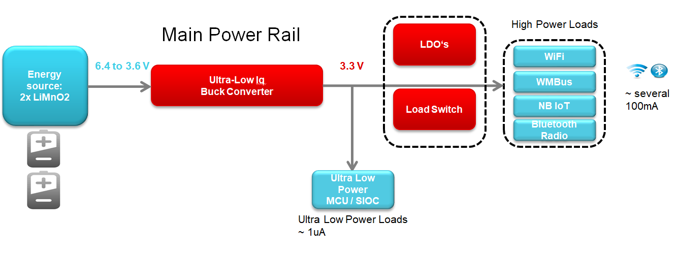
Many battery-powered applications require a step-down buck converter to work in 100% duty-cycle, where VIN is close to VOUT, in order to extend battery run time when battery voltage is at its lowest value. For example, let’s say that there are two lithium manganese dioxide (Li-MnO2) batteries powering a smart meter. Li-MnO2 batteries are primary non-rechargeable cells used increasingly in smart gas or water meters because of their long operational lives (as much as 20 years) while being more cost-effective than lithium thionyl chloride batteries. Figure 1 shows the system configuration of two Li-MnO2 cells placed in series (2s1p) and then stepped down to power a microcontroller.

A smart meter power architecture

Figure 1: A smart meter power architecture

Ultra-low quiescent current (IQ) DC/DC converters can help you design applications with a battery lifetime up to 20 years. The load profile of a smart meter application is not a continuous load but a variable load profile. In order to enable long battery life, the system will draw a high current only occasionally (to send a wireless signal or actuate a valve), and then go back to a very low load condition. This type of load profile enables low average current consumption in the microampere range. High efficiency at such light loads requires ultra-low IQ, especially during the off-time where current consumption could be much lower than the average current consumption.  TI’s TPS62840 ultra-low power buck converter has an operating IQ of only 60 nA and can regulate a 3.3-V power rail. The TPS62840’s very low IQ in 100% mode – 150 nA – further extends battery run time.

To better help you design and simulate your ultra-low power-supply circuit, WEBENCH® Power Designer is an online tool that enables the creation of customized power supply designs based on your specifications.

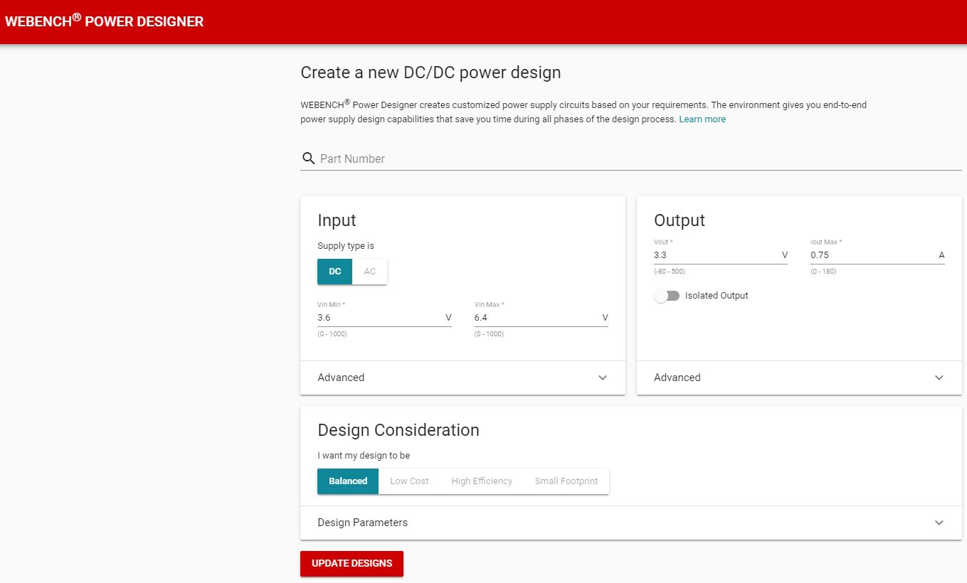
In our example, the average voltage per cell is around 3.0 V. The initial voltage of a cell is approximately 3.2 V when fresh, and the voltage can drop to less than 2 V when fully discharged. Assuming that each battery discharges down to 1.8 V and is 3.2 V when fresh, enter these parameters into WEBENCH Power Designer (Figure 2).

Design specification entered in WEBENCH Power Designer

Figure 2: Design specification entered in WEBENCH Power Designer

Using a 3.6-V minimum input voltage in the WEBENCH Power Designer search tool yields 51 possible devices, but the TPS62840 is not one of them. Why is that?

WEBENCH focuses on two initial parameters to help you find the best device for your system:

1. VINMIN> VOUT is the first check WEBENCH Power Designer looks for in the user inputs for buck converters topologies. If VINMIN > VOUT, then WEBENCH Power Designer selects buck converters as part of the solutions list. If VINMIN≤ VOUT, WEBENCH Power Designer recommends buck-boost converters to regulate your VOUT instead of buck converters that operate in 100% Duty Cycle mode. This is because WEBENCH wants to give you a solution where your VOUT is regulated even when VINMIN ≤ VOUT.

2. After passing the first check, the second check verifies if the calculated duty cycle is greater than the max duty cycle specified in the buck converter datasheet. For buck converters that can operate in 100% duty cycle mode, 99.9% is used as the threshold. Losses are included when calculating the duty cycle. This increases the calculated duty cycle in WEBENCH Power Designer far above the ideal VOUT/VIN.

After selecting numerous devices, WEBENCH Power Designer performs detailed designs for each device. Below are three different outcomes which can be observed depending on the input parameters used:

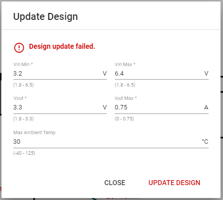
  • VIN from 3.2 V to 6.4 V, IOUT_MAX = 0.75 A and VOUT = 3.3 V in the TPS62840 WEBENCH Power Designer model (Figure 3).

Error message that the input voltage is too low

Figure 3: Error message that the input voltage is too low

The design update is failing because the minimum VIN is lower than VOUT. This design does not pass WEBENCH’s first check.

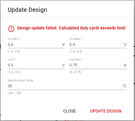
  • VIN from 3.6 V to 6.4 V, IOUT_MAX = 0.75 A and VOUT = 3.3 V in the TPS62840 WEBENCH Power Designer model (Figure 4).

Error message that the duty cycle is too high

Figure 4: Error message that the duty cycle is too high

The design does not update because the duty cycle when calculated includes losses such as the high-side MOSFET RDSON and inductor DCR. Here, the duty-cycle value is greater than 99.9%. This design does not pass WEBENCH’s second check.

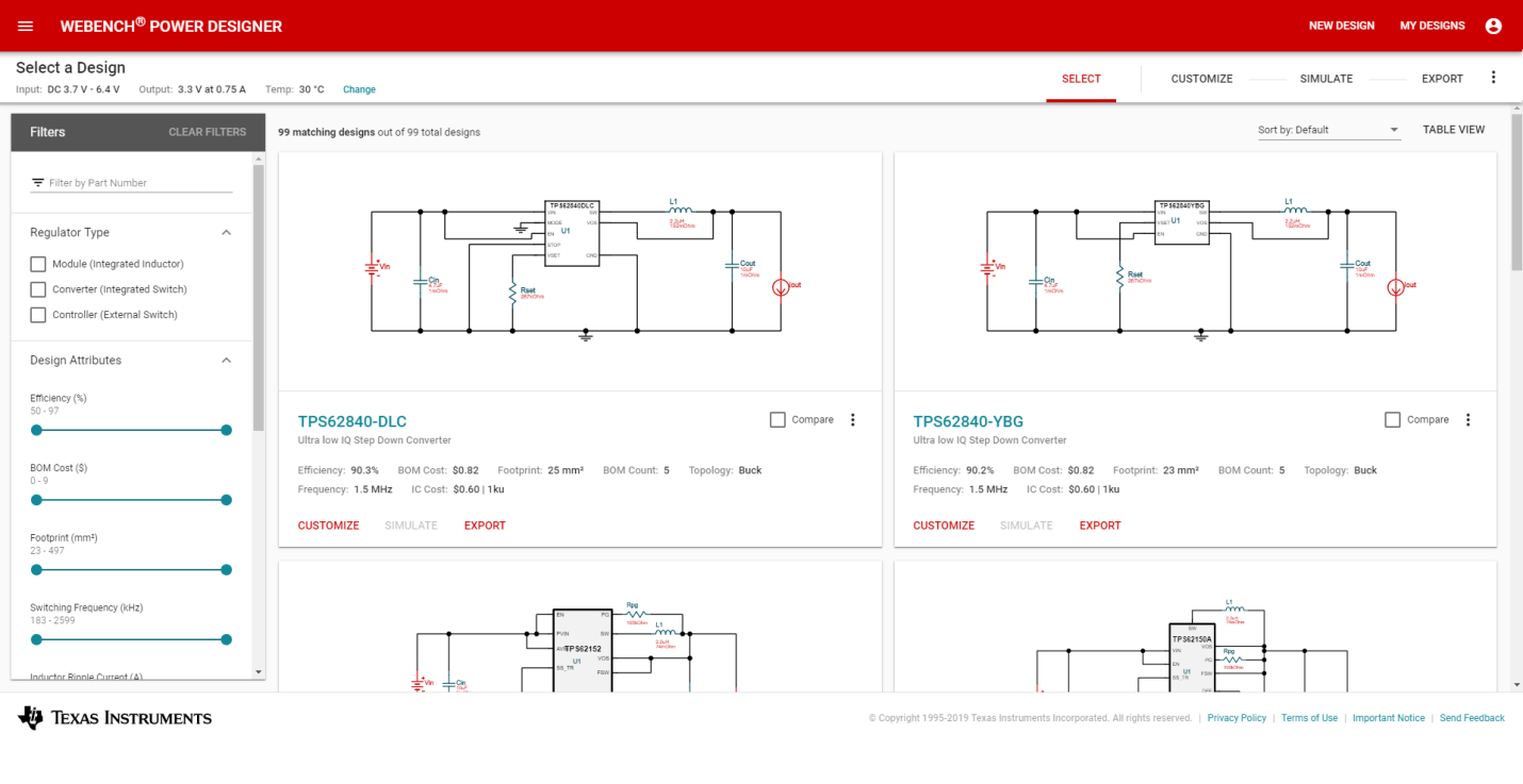
  • VIN from 3.7 V to 6.4 V, IOUT_MAX = 0.75 A and VOUT = 3.3 V on the WEBENCH Power Designer Select a Design screen (Figure 5).

The TPS62840 displayed in WEBENCH Power Designer

Figure 5: The TPS62840 displayed in WEBENCH Power Designer

The final example displays the TPS62840 since the design passed both checks.

Tips to use WEBENCH Power Designer more effectively when close to 100% duty-cycle:

  • Add a sufficient delta between the input voltage and the output voltage to reduce the duty cycle.
  • Reduce the output current to reduce losses and reduce the duty cycle.

Either of these solutions enable WEBENCH Power Designer to design with the TPS62840. In an actual application, operating in 100% mode is normal and generally acceptable in order to fully discharge the battery. In 100% mode, the output voltage of a step-down converter decreases as the battery voltage decreases. This can still fit the system specifications of most loads.

Additional resources

Real-time control meets real-time industrial communications development – part 4

$
0
0
Part 1 of this blog series gave an overview of the market opportunities for EtherCAT slave stack support on C2000™ microcontrollers (MCUs) and an introduction to a three-phased solution to jump-start slave stack development. Part 2 detailed what’s...(read more)
Viewing all 4543 articles
Browse latest View live


<script src="https://jsc.adskeeper.com/r/s/rssing.com.1596347.js" async> </script>