Quantcast
Channel: TI E2E support forums
Viewing all 4543 articles
Browse latest View live

So, what's the deal with frequency response?

$
0
0

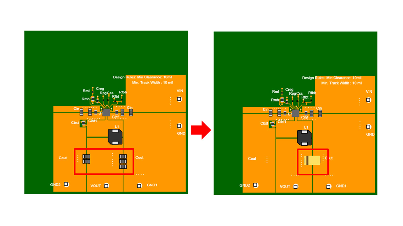
[[This article is the third installment of a series that explains how to use scattering parameters, also known as S-parameters, in the design of direct radio-frequency (RF) sampling architectures. The first installment is here.]]

Frequency response is the ratio of the reflected wave at the output port to the incident wave at the input port. The VNA can directly measure the incident wave, but it cannot measure the reflected wave since it is contained in the ADC’s digital output stream.

This can be solved by capturing the ADC samples and processing them to determine the reflected wave. Before combining to calculate frequency response we need to take care of a few calibration issues.

First, SOLT calibration only corrects for ratios required for S-parameter measurement (with the reference plane at the end of the test cables). The actual incident power must be known in absolute terms, since the ratio must be computed from two sources.

Secondly, port extension cannot be used since this is not a self-contained VNA measurement function.

Finally, we do not know the phase between the incident wave at the ADC inputs and the resulting capture event at the FPGA capture card.

Taking this step by step, Figure 6 shows the measurement setup. To obtain the frequency response, we calibrate the VNA using the SOLT standards, which places the reference plane at the end of the VNA cables. The impact of the connector and traces on the test fixture will be compensated for in post processing, which will be discussed shortly.

Figure 1: Frequency response measurement setup

Figure 1: Frequency response measurement setup

As we mentioned SOLT calibration only corrects for wave ratios. To measure absolute quantities, you need to perform power calibration which entails connecting a power meter to each test port at the end of the test cables. The VNA executes a routine to adjust the incident power at each test frequency to the desired value while compensating for the incident wave measurement bridge.

The zero length through (ZLT) structure is included on the test fixture to compensate for the interconnect between the connectors and DUT. The ZLT is equivalent to a pair of reflect structures connected back to back, which can be used to measure the loss between the test cables and the DUT terminals. To estimate this, we measure the insertion loss of the ZLT vs. frequency and then divide by 2 to find the loss from the connector to the DUT terminal.

Using the ZLT for this purpose is only valid if the return loss of the test fixture is sufficiently low enough that errors due to mismatch are negligible, which can be verified by measuring the ZLT’s return loss.


Designing for demanding requirements?

 Test and measurement iconMeet the requirements of tomorrow's test and measurement applications with the fastest-ever ADC. 

Measuring the frequency response

To take a frequency response measurement, the VNA is placed in constant wave mode so that the stimulus frequency can be manually swept while capturing the data with the FPGA capture card. The VNA and ADC clock source are synchronized to enable un-windowed fast Fourier transform (FFT) estimation of the amplitude.

We can then collect the incident wave amplitude (in dBm) and the FFT fundamental level (in dBFS) and form a ratio. To finish the measurement, we subtract half the ZLT insertion loss at each frequency and normalize to the amplitude at the starting frequency. Figure 2 shows the result.

Figure 2: ADC12DJ3200 frequency response measurement in dual-channel mode

Figure 2: ADC12DJ3200 frequency response measurement in dual-channel mode

Note that this is a scalar measurement, because there is no straightforward way to know the phase between the VNA and the FPGA capture card. We are currently investigating methods to measure the relative phase which could mitigate the standing wave issue.

 Putting everything together for an S-parameter model

S-parameter models are typically represented in the Touchstone text file format. Figure 3 shows this file format, which is organized into columns. The first line of the file indicates that this is an S-parameter measurement, with frequency units of hertz, magnitude/angle format and a port impedance of 100 Ω.

Figure 3: Touchstone model format

Figure 3: Touchstone model format

The first column gives the stimulus frequency, followed by two columns for each S-parameter (in this case magnitude and angle). The first two columns take data from the input impedance measurement; the next two columns are from the frequency response; and the final four columns are set to zero since port 2 is digital (that is, the reflection coefficient and isolation are perfect).

Figure 4 shows how the model is used in Keysight ADS. Port 1 is the ADC RF input and port 2 is the digital output. The RF input is represented as a single-ended port to simplify model creation. An ideal transformer is added to convert the input back to differential.

 Figure 4: Final S-parameter model simulation setup

Figure 4: Final S-parameter model simulation setup

Figure 5 shows the simulated model for the ADC12DJ3200. This ADC can operate in dual-channel mode at 3.2 GSPS or single-channel dual-edge sampling (DES) mode at 6.4 GSPS.

Figure 5: Final S-parameter model simulation results

Figure 5: Final S-parameter model simulation results

 Conclusion

The approach we’ve described in this article makes it possible to construct very useful models of high speed ADCs for system-level or PCB designs. In the next installment of this series, we’ll show how to put the model to work in the design of a receiver front-end PCB design.


How using bi-directional DC/DC converters for an elevator automatic rescue device improves efficiency and reduces cost

$
0
0
Because elevators transport millions of people every day, operational safety is of prime importance. Have you ever thought about what happens when the mains supply to the elevator shuts down? Will the elevator drop down the hoist way, or get stuck somewhere...(read more)

Overcoming design challenges for low quiescent current in small, battery-powered devices

$
0
0

Thanks to advances in miniaturization, Bluetooth® communication and embedded processing, modern hearing aids have more features than ever, from streaming music to being able to adjust hearing amplification from an app on your smartphone.

These increased capabilities come at a price, however: modern features require more power. Increased power consumption is a challenge for engineers designing hearing aids, primarily because older versions use disposable zinc air batteries. These batteries typically last about two weeks. But when you add more features to hearing aids, such as giving them the ability to play music, the battery life could drop down to hours. Thus, engineers are using rechargeable lithium batteries in their next-generation hearing aid designs.

Rechargeable lithium batteries increase the power system complexity in a variety of ways, the most important being how to safely and accurately charge the battery. There are also extra design considerations when using two hearing aids. Because the left and right earpieces have no physical connection, it is not possible to charge both of them through a single cable simultaneously. So almost all new hearing aids are now equipped with a case that has both charging and storage functions.

This case is designed with specific sockets for each earpiece to ensure proper charging. The charging for the earpieces must be precise, since rechargeable hearing aids are typically 25 mAh-75 mAh and the charging case ranges from 300 mAh-70 0mAh. This translates to about 24 hours of usage for the earpieces and about 10 recharge cycles from the case, before the case itself needs to be re-charged.

With a charging case, hearing aid designers now have three different lithium batteries to consider: one for the case and two for the earpieces. The choice of battery chargers plays a significant role in the design.

It is also critical to note that charging a battery from a battery (i.e. charging the earpiece battery from the charging case battery) is not as simple as charging from the wall, since the voltage difference between the two batteries will not be very large. There has to be internal circuitry to boost the voltage difference between the charging case and the earpieces to enable full charging. As the battery discharges, its voltage is slowly dropping. Looking at the discharge curve shown in Figure 1, at around 50% of battery capacity, the charging case voltage would be at around 3.6 V. But that means that without a boost, the charging case can only charge the earpieces up to 3.6 V, even when the energy stored in the case is sufficient to charge them fully.

Figure 1: A sample battery discharge curve for a lithium-ion battery; the typical mean point voltage is 3.6 V and the end-of-discharge voltage is 3 V (Source: “Characteristics of Rechargeable Batteries”)

In such a scenario, most engineers would think to use a discreet boost. While a discreet boost does work, it typically increases solution size and inefficiencies by adding an additional boost and inductor component to the power architecture.

To overcome these challenges, consider on-the-go charging supported by quiescent currents. For example, TI’s BQ25619 battery charger and BQ25155 linear charger support charging without an external boost. In the hearing aid application, you could place the BQ25619 in the charging case and the BQ25155 within each earpiece.

Then, instead of always boosting the charging case output to 5 V, you would instead boost to the minimum voltage necessary to allow sufficient headroom between the charging case and earpiece batteries using the BQ25619’s boost functionality. This reduces the power loss of unnecessary boosting and also increases earpiece charging efficiency, since the voltage differences are reduced.

The BQ25155 is a good fit for the earpieces, since its 3.4-V input voltage minimum allows longer charging without the boost, and its 43-µA quiescent current increases battery run time. Meanwhile, the BQ25619’s 7-µA quiescent current in ship mode maximizes charging case shelf life. The BQ25619’s 20-mA charge termination current enables it to charge small-sized batteries with 7% more capacity.

The good news is that these benefits are not limited to hearing aids: all two-battery device systems, including earbuds and wearable patches, can benefit from these innovations. TI will continue to implement two-charger configuration in future designs with features like:

  • Higher efficiency charging for both the earpieces and charging case while providing battery monitoring and protection, and reducing the total bill of materials with an integrated boost.
  • Pin reduction for earpieces and charging cases by requiring only one line of communication.

With the BQ25619 and the BQ25155, you can improve the amount of charge cycles that are extractable from a charging case without increasing cost or solution size.

Additional resources

Leveraging MSP430™ FRAM MCUs with integrated configurable analog in modern-day factories

$
0
0

Most revolutionary changes in factories can be traced back to some groundbreaking innovation. Whether harnessing the power of steam in the mid-18th century or developing the assembly-line production model in the early 20th century, every innovation has led to radical efficiency and productivity improvements.

We are in an era where the innovation of industrial robotics, intelligent sensors and automated assembly lines are fundamentally changing the way factories are run. The process of manufacturing a product has become more and more automated, with machines learning how to do work typically done by hand. Sensors continuously monitor these machines, measuring parameters such as vibration and temperature, in order to ensure that they are operating properly and not overheating. These sensors then transmit their information to a central hub that oversees all of the machines in its assembly line. It is essential that such complex networks of systems communicate with each other in a way that keeps everything running smoothly.

This need for efficient communication is where the standardization of factory automation communication protocols really starts to shine. Three of the most common wired communication protocols used by field transmitters in modernized factories – IO-Link, 4-20 mA and Highway Addressable Remote Transducer (HART) – can all be implemented using MSP430™ ultra-low-power microcontrollers (MCUs) with integrated configurable analog signal-chain peripherals. One of these configurable analog signal-chain peripherals is the Smart Analog Combo whose block diagram is shown below.

Figure 1: Smart Analog Combo featured in the MSP430FR235x device family

Paving the way for what is known as Industry 4.0, IO-Link is gradually becoming one of the most widely adopted communication protocols in factory automation. It is based on point-to-point communication and enables bidirectional communication between sensor nodes and their IO-Link master. One of the most compelling arguments for IO-Link is having the ability to reprogram a sensor node or update configuration parameters on the fly. An IO-Link firmware update of a typical device with flash memory can take up to 1 minute due to slower write speeds and the need for a “busy” message to be sent to the master. MSP430 ferroelectric random access memory (FRAM)-based MCUs make updating firmware a piece of cake, with write speeds up to 100 times faster than flash, in addition to lower power and advantages in reliability and security. You can write data to FRAM right out of the IO-Link channel with no buffering required, thus making it superior to flash for firmware updates.

The IO-Link Firmware Update Reference Design Leveraging MSP430 FRAM Technology, based on the MSP430FR5969 MCU, showcases the benefits of using an MSP430 FRAM-based MCU for IO-Link firmware updates. The IO-Link software stack used by this reference design, depicted below, is provided by a third-party company and is compliant with IO-Link specifications v1.1 and v1.0.

Figure 2: IO-Link Firmware Update Reference Design Leveraging MSP430 FRAM Technology

Although IO-Link is building momentum, 4-20 mA is still one of the most dominant standards in the industry. The 4- to 20-mA current loop enables a sensor to transmit information to a host receiver that can be located up to thousands of meters away. The low-power requirements of current-loop transmitters make MSP430 ultra-low-power MCUs a perfect fit for loop-powered sensor applications. The 4- to 20-mA Loop-Powered RTD Temperature Transmitter Reference Design with MSP430 Smart Analog Combo, shown in Figure 3, showcases the benefits of using the MSP430FR2355 for a current-loop transmitter. Rather than taking up space on a board for a custom analog front end to drive the current loop, it is driven by the configurable operational amplifier block inside of the MSP430FR2355 MCU, which also features a built-in digital-to-analog converter and programmable gain stage. MSP430FR235x MCUs include four Smart Analog Combo blocks that when used independently or together enable a wide variety of signal-conditioning and signal-amplifying functionalities.

Figure 3: 4- to 20-mA Loop-Powered RTD Temperature Transmitter Reference Design with MSP430 Smart Analog Combo

The last protocol widely used in factory automation is the HART protocol, which is heavily based on the legacy of 4- to 20-mA analog current loops. HART is considered to be a “smarter” version of the current loop because in addition to providing information over the standard current loop, it also overlays low-frequency ones (1200 Hz) and zeros (2200 Hz) on top of the analog current signal, providing additional information to the master hub. This enables sensors to communicate more intelligently. The Highly-Accurate, Loop-Powered, 4-mA to 20-mA Field Transmitter with HART Modem Reference Design showcases the MSP430FR5969 in a field transmitter application where the data link layer and application layer of the HART protocol are both implemented on the MSP430 MCU by leveraging a HART software stack written and provided by a third party company.

Figure 4: Highly-Accurate, Loop-Powered, 4-mA to 20-mA Field Transmitter with HART Modem Reference Design

By using the communication protocols discussed in this article, industrial remote transmitters can operate seamlessly, allowing factories to become even smarter and more efficient.

Additional resources

How connected vehicles leverage data: 3 common questions

$
0
0

Connected driving, even though it exists today, still has a long way to go. In the future, vehicles will communicate with the driver, other cars, the road and surrounding infrastructure, pedestrians, and the cloud, all while giving passengers a constant connection.

Thanks to these increasing levels of connectivity, vehicles will be able to receive, interpret and transmit data – both within the vehicle as well as with the world around it – to inform driving decisions, increase passenger convenience and enable increasing levels of autonomy.

Let’s tackle three common questions about the future of connected vehicles.

Q: What is V2X, and how does it relate to the connected car?
A: Vehicle-to-everything (V2X) is a multipoint network that allows information to pass between a vehicle and the world around it, including pedestrians, the surrounding infrastructure (such as light posts, traffic signals and parking lots), other vehicles and the cloud/network. Figure 1 shows this ecosystem.

Figure 1: V2X includes vehicle-to-cloud (V2C), vehicle-to-infrastructure (V2I), vehicle-to-pedestrian (V2P) and vehicle-to-vehicle (V2V) connectivity

Central to the V2X network is the telematics control unit (TCU), the brain of the telematics system, which serves as the central hub for nearly anything and everything that talks wirelessly to the car from the outside world.

Q: What’s the difference between DSRC and C-V2X?
A: Dedicated short range communication (DSRC) and cellular V2X (C-V2X) are two types of radio technologies that are competing to become the standard for V2X connectivity. Table 1 outlines some of the trade-offs of each technology.

DSRC C-V2X
Communication technology using the Wi-Fi IEEE Institute of Electrical and Electronics Engineers 802.11p standardCellular LTE standard driven by the 5G Automotive Association

Advantages:

  • Permits low latency (2-ms) communication for basic V2I and V2V safety messages.
  • Widely used, tested and reliable (~20 years).
  • Complements LIDAR and radar in advanced driver assistance systems (ADAS) well.
  • Interoperability with V2I and V2V systems.

Advantages:

  • Lower latency and two times the range of DSRC (can exceed 1 mile), even without a network connection.
  • Able to use all features in the existing LTE network.
  • Able to connect to anything (V2I, V2V, V2P and more).
  • Better suited to systems around the globe.

Disadvantages:

  • DSRC is an older technology that doesn’t have latency as low as C-V2X.
  • Some opponents say there is no room for evolution.

Disadvantages:

  • Doesn’t yet have government regulatory backing.
  • Could have interoperability issues.

Table 1: Trade-offs between DSRC and C-V2X for automotive applications
(Data sources: 5G Automotive Association and Electronic Design)

Q: What are some of the key domains that manage data within the vehicle?
A: Once the vehicle receives data from the outside world, there are several domains called gateways that are responsible for safely and securely transferring data within a vehicle. There is the potential for several gateways within the vehicle: a centralized gateway and multiple domain gateways. These gateways may include:

  • An automotive gateway– a central gateway module that manages and routes data to various network domains within the vehicle.
  • A smart telematics gateway– this gateway represents the next evolution of highly integrated TCUs—the infotainment gateway module within the digital cockpit that manages communications between the central gateway and the outside world, including emergency calling (eCall), vehicle tracking, electronic tolls, diagnostics and over-the-air updates.
  • An ADAS domain controller– an ADAS gateway module that manages communications between the central gateway and powertrain systems to enable different levels of autonomous driving.

The race is on to design a connected vehicle that delivers a driving experience like none we have experienced before. I look forward to the day when this additional connectivity adds a predictive quality to the reactiveness of autonomous driving – making the road safer for drivers and pedestrians.


Additional resources

Non-contact and private stance detection with TI mmWave sensors

$
0
0
This article was co-written by Keegan Garcia According to Forbes , by 2050, the global population of people over the age of 60 is expected to hit 2 billion. To put this into perspective, this will represent over a fifth of the world’s population...(read more)

VIDEO: Wi-Fi security challenges and FIPS Validation

$
0
0

What does it take to meet the Federal Information Processing Standards (FIPS)?  What does FIPS Validated mean? Do you need it?  Andrew joins Nick and me in this Connect episode to dig deeper into Wi-Fi security challenges and wireless MCUs. The SimpleLink™Wi-Fi CC3135 and CC3235 devices are the first FIPS validated wireless SoCs available today. 

(Please visit the site to view this video)

Understanding the difference between capacitors, capacitance and capacitive drop power supplies

$
0
0

Knowing the difference between a capacitor’s rated value and its actual capacitance is key to ensuring a reliable design. This is especially true when considering high-voltage capacitors used in capacitive drop power supplies for equipment like electricity meters, since losing too much actual capacitance may result in insufficient power to support the application.

With a capacitive drop power supply, the high-voltage capacitor is typically the largest (and one of the more expensive) components in the circuit. When sizing capacitors, it is essential that the actual capacitance can support the load current that the design requires.

Figure 1 shows the existing capacitance values of capacitors available from a capacitor manufacturer, Vishay. Let’s assume that your design calculations show that your design requires a 1-µF capacitor (90 VAC_RMS at 60 Hz and 5 VOUT @ 25 mA). Considering the available capacitors, you might choose a 1.2-µF capacitor to accommodate the manufacturer’s tolerance of 20%. However, taking into consideration the capacitor’s tolerance and aging effects, you may see a 50% reduction in the actual capacitance of your capacitor over time. In other words, in the worst-case scenario, the 1.2-µF capacitor you chose may only have 0.6 µF of capacitance at its end of life. 

 Figure 1: Sample range of high-voltage capacitors available from manufacturer Vishay

Wait, aging is an issue? If the application is expected to work for 10-plus years, it is not unreasonable to assume that film capacitors may lose ~25% of their capacitance over the lifetime of the product, due to operating temperature, load current and humidity. Table 1 shows a prediction of the total capacitance after considering worst-case tolerance and aging.

Table 1: Tolerance and aging effects on actual capacitance

Considering the effects of the tolerances, the best choice to support a 25-mA load at 5 VOUT in a traditional capacitive drop architecture, is a 2.2-µF capacitor, which comes with serious size implications. Is there a better way?

One way to mitigate the effects of capacitance loss due to aging is to simply use a lower-value capacitor. For example, if you used a step-down converter to reduce a DC-rectified 20 V down to 5 V, with perfect efficiency you could maintain 25 mA at the 5-V output, but you would only need to size the high-voltage capacitor to support 6.25 mA. To clarify – in the above example, if a linear power solution required 1 µF, a four-time reduction in voltage will yield a four-time increase in load current capability. In this example, 1 µF reduces to 0.25 µF.

Looking at the same derating for tolerance, you would calculate the need for a 0.3-µF capacitor, yet the next available capacitor has a value is 0.33 µF. Add to that the aging effects, and the next available capacitor you should consider is actually 0.47 µF.

The only problem with using a DC/DC step down converter in applications like electricity meters is that they tend to require a very high level of tamper immunity. This means preventing external magnetic fields from impacting the design’s additional circuitry like Hall-Effect sensors or a tamper-proof enclosure is required, which will add additional cost.

One way to resolve the issue of the oversized capacitor and still support tamper immunity is to use a nonmagnetic step-down converter. TI’s TPS7A78 voltage regulator requires no transformers or inductors to produce a nonisolated low-voltage output. The TPS7A78 reduces a 2.2-µF capacitor to 0.470 mF, guaranteeing 25 mA of load current over the life of the product. Figure 2 compares the area and volume of the two capacitors.

Figure 2: Area and volume comparison of two high-voltage capacitors

So why do smaller capacitors matter? The obvious answer is the overall solution size. But the less obvious benefits are standby power and efficiency. Reducing the amount of capacitance required by four times reduces standby power from ~300 mW down to ~77 mW. Adding the intelligent clamp circuit behind the TPS7A78 supporting a 25-mA load cuts down the total standby power to ~15 mW.

Knowing how to minimize the capacitor to ensure enough capacitance saves cost for both the manufacturer and the consumer when using capacitive drop power supplies.

Additional resources


Getting the most out of your power stage at the full temperature range – part 2

$
0
0
In part 1 of this series, I described a situation in which you are designing a power stage for motor control with high efficiency. To ensure that the power stage is only used under recommended temperatures, a temperature sensor monitors the temperature...(read more)

Driving industrial innovation with TI small-size sensors

$
0
0

Note: Will Cooper and Robert Ferguson co-authored this technical article.

Trends in small consumer electronics have disrupted the industrial world, spiking a demand for smart but compact devices that enhance manufacturing (like proximity sensors in factory settings) and daily life (like temperature or magnetic sensors in consumer applications like refrigerators or vacuum robots). To achieve the smaller designs these applications require, design engineers must choose more compact chip sensors that deliver high accuracy in tiny form factors without sacrificing efficiency.

In this article, we will review advancements in industrial applications made possible by the smallest sensors on the market today – in this case temperature, Hall-effect and millimeter-wave (mmWave) sensors.

Designing with small-size temperature sensors

Many industrial applications depend on reliable and consistent system hardware. Some of the biggest challenges design engineers must account for include changes in temperature that could degrade batteries or damage critical components in extreme temperature environments. Therefore, preemptive actions like warming or cooling a system must occur before the processor powers up.

With configurable temperature thresholds and built-in hysteresis, you can directly connect temperature switches to the enable pins of a power supply or general-purpose input/output interrupt of a microcontroller (MCU) in order to take immediate and autonomous action to protect a system. This implementation can reduce or eliminate the dependence on software, providing both reliability and a shortened development cycle.

The TMP390 temperature switch, shown in Figure 1, offers fully integrated dual-channel threshold monitoring and built-in trip test. This solution enables over 60% area savings compared to an equivalent discrete implementation using negative temperature coefficients (NTCs), while significantly decreasing component count. Integration also brings the advantage of guaranteed temperature monitoring accuracy, with a variation of only ±1.5°C from 0°C to 70°C and ±3°C from -55°C to 130°C. Such high accuracy means that you can protect systems without sacrificing performance due to extensive temperature guard-banding in case of measurement uncertainty.

Figure 1: Schematic and layout of a discrete dual-threshold detection circuit and the integrated TMP390 temperature switch

Designing with small-size Hall-effect sensors

Industrial innovation often calls for better performance, higher efficiency and longer battery life; yet more often than not, squeezing these improvements into smaller form factors remains challenging. Brushless DC (BLDC) motors used in medical or dental care products, for example, do a good job of translating high-functioning requirements into tiny motors with diameters less than 10 mm.

For motor commutation in small motor designs, the built-in electronics – such as Hall-effect latch sensors – must be small. To address this requirement, TI has introduced the DRV5011 Hall-effect latch (see Figure 2).

Figure 2: The tiny DRV5011 wafer chip-scale package compared to coins for reference

The low-profile DRV5011 supports the use of smaller magnets and offers more design flexibility. For example, it becomes possible to manufacture rotary dials used to adjust volume or electronic settings within a specific application with a smaller magnet to detect speed, direction and position, or the dial can be placed further away due to the DRV5011’s high sensitivity.

Table 1 lists additional end products that can take advantage of the small size of the DRV5011.

End product

DRV5011 benefits

Handheld drills

Enables the necessary placement of three Hall-effect latches on a board to monitor the speed, direction and location for the commutation of a small BLDC motor.

Vacuum robots

Two DRV5011 sensors can easily measure the speed and direction of the wheels. Their small size supports flexibility in board placement.

Table 1: Common products that benefit from small-size Hall-effect sensors

Designing with small-size TI mmWave sensors 

As more industrial applications move toward autonomous functioning, it’s becoming increasingly important to design devices with highly accurate sensors that can generate and process a variety of data at speed to make real-time decisions. In a factory setting, for example, it’s important that industrial robots sense and respond to nearby human activity.

Antenna configuration with TI mmWave sensors determines the maximum object range, maximum field of view and the resolution to cover a wide area for simultaneous object detection. As shown in Figure 3, our small-size antenna-on-package (AoP) sensors enable designs in form factors that were never possible before for industrial sensing. TI mmWave AoP sensors offer all of the benefits of a complete radar sensor while simplifying the manufacturing and testing process with an easy-to-use MCU-like FR4 board.

Figure 3: TI’s mmWave AoP evaluation module reduces board space while adding temperature sensing with the TMP112A (right)

In addition to simplifying design, manufacturing and testing, AoP design also reduces overall antenna size by integrating the antenna onto the device, saving board space previously allocated for the antenna.

Regardless of the end device or real-world application, a wide variety of sensing technologies can support highly accurate, high-speed readings in the smallest of sizes. With so many options, design engineers shouldn’t have to sacrifice one benefit over another. Our portfolio of small-size sensors helps engineers get real-time information, autonomous protection, and improved system productivity and performance.

Additional resources

From concept to cosmos: How Jack Kilby's integrated circuit transformed the electronics industry

$
0
0


In 1958, as one of the few employees working through summer vacation at our company, electrical engineer Jack Kilby had the lab to himself. And it was during those two solitary weeks that he hit upon an insight that would transform the electronics industry.

Since 1948, transistors had begun to replace large, power-hungry vacuum tubes in electronics manufacturing, but hand-soldering thousands of these individual components onto a chip was expensive, time-consuming and unreliable.

Jack’s insight was that the same semiconductor materials used to make transistors could be tweaked to produce resistors and capacitors, too. This meant an entire circuit could be produced from a single slice of semiconductor material.

Later that year, on Sept. 12, Kilby presented his invention: An electronic oscillator formed from a small slice of the semiconductor material germanium. The first integrated circuit was born, bringing with it the exponential growth of the electronics industry and the spread of electronic devices throughout every aspect of our lives.


 Learn how Jack Kilby’s integrated circuit and our people helped land man on the moon 50 years ago.


Unleashing creativity in electronics

Our company needed a showcase device, something that could prove the integrated circuit's potential to take large, unwieldy and expensive technology out of specialized computing labs and into the wider public's offices, homes and pockets. They settled on a hand-held calculator.

Jack KilbyAt the time, a calculator was a large desktop machine that required a constant AC power supply. When our prototype was unveiled in 1967, it used just four integrated circuits to perform addition, subtraction, multiplication and division. It weighed 45 ounces and could fit in the palm of your hand.

Chip complexity began to grow exponentially, now that the creative energy of electronics engineers was finally unleashed from the constraints of wiring together individual transistors. The most significant result was the creation of the first microprocessor, which packed the workings of an entire central processing unit into less than a square inch – and supported the development of the first portable computers.

Circuits in space

The miniaturization of electronics came in handy for coordination of the first moon mission, since the idea of launching the car-sized mainframes used by NASA's ground control up on a rocket itself was both physically and economically impossible.


Instead, the space agency created the world's first integrated circuit-based spaceflight control system, the Apollo Guidance Computer. In July 1969, running around 145,000 lines of code with 12,300 transistors, this 70-pound computer successfully coordinated both Neil Armstrong and Buzz Aldrin's arrival on the moon – and their safe return to Earth eight days later.

Ubiquitous Computation

Chips many thousands of times more powerful than those used in the Apollo Guidance system can now be found everywhere from factory robots to car dashboards, cell phones, computers, smart watches and smart speakers. They can even be found inside the ears of millions of people around the world in the form of hearing aids.


Forty-two years after that pivotal couple of weeks in 1958, Jack accepted half of the Nobel Prize in physics for his invention. In his acceptance speech, he reflected on the host of electronics innovations that have been developed since – far beyond what he’d imagined possible at the time: "It's like the beaver told the rabbit as they stared at the Hoover Dam. 'No, I didn't build it myself, but it's based on an idea of mine.'"

Options for reducing the MLCC count for DC/DC switching regulators

$
0
0

Multilayer ceramic capacitors (MLCCs) are popular in electronic circuits, particularly for decoupling power supplies, but have become harder to procure due to a severe market shortage of MLCCs in larger case sizes, which began in 2018. Market indicators show that nothing will change until at least 2020. Consequently, designers are now seeking ways to reduce the number of MLCCs in DC/DC switching regulators.

One option to minimize the MLCC count for DC/DC switching regulators is to select a device capable of operating with fewer external capacitors. Another option is to choose a DC/DC switching regulator with TI’s D-CAP+™ control mode. Increasing the switching frequency will also help reduce capacitor count. For example, increasing the switching frequency of the TPS563201 from 580 kHz to 1.4 MHz led to the design of the TPS563249, which has one less capacitor.

The option for reducing the MLCC count for DC/DC regulators studied in this article considers the use of a replacement technology. The most common types of replacement technologies are film, aluminum (liquid and polymer), and tantalum (solid and polymer). There are pros and cons of each technology, including their capacitance, voltage range, equivalent series resistance (ESR), size, and current rating. When selecting capacitors for DC/DC switching regulators, ESR is usually the biggest differentiating factor because the higher it is the more output-voltage ripple, heating, and input noise occur, which is why MLCCs are popular for DC/DC switching regulators since they most often have the lowest ESR. Aluminum polymer capacitors share several characteristics with MLCCs and have a low enough ESR to be a replacement for MLCCs amongst designers. As you can see in Figure 1, aluminum polymer capacitors are the type of capacitors that have the closest ESR values to MLCCs.


Figure 1: ESR of various capacitor technologies (source: Why low ESR matters in capacitor design)

One downside of aluminum polymer capacitors is that they are bigger than MLCCs. When using the WEBENCH® Power Designer tool, which provides printed circuit board (PCB) layout information, you can see in Figure 2 that if you replace the five output MLLCs of the TPS568215 synchronous buck converter with one aluminum polymer capacitor, both solutions occupy similar surface areas.

Figure 2: Replacing MLCCs with an aluminum polymer capacitor for the TPS568215 in the WEBENCH Power Designer tool

The question now comes down to performance. How do aluminum polymer capacitors compare to MLCCs, and can they truly replace MLCCs without forcing designers to make too many compromises?

To get a rough idea, I used the WEBENCH Power Designer tool to simulate some load transient responses. As shown in Figure 3, using an aluminum polymer capacitor at the output instead of the MLCCs increases the output voltage ripple tenfold. Thus, replacing MLCCs with only aluminum polymer capacitors is not a feasible option if you need decent performance.

Figure 3: Load transient simulations run on the WEBENCH Power Designer tool for the TPS568215 with output MLCCs (a); and aluminum polymer capacitors (b)

What about combining MLCCs and aluminum polymer capacitors to help reduce the voltage ripple while minimizing the ceramic count on DC/DC switching regulators? To determine that, I performed some real PCB testing with the TPS568215 evaluation module (EVM). The strategy was first to run some tests on the initial configuration of the EVM to validate the test setup by comparing the input voltage ripple, output voltage ripple, load transient response, start up response, and shut down response with the ones from the datasheet. Then, I tried out different capacitor configurations both at the input and output of the EVM.

The two setups that showed the closest results to the initial configuration were using a mix of aluminum polymer capacitors and MLCCs, as shown in Figure 4, where the setup in Figure 4a tested the output voltage ripple and the setup in Figure 4b tested the input voltage ripple.

Figure 4: TPS518215EVM setup with one aluminum polymer capacitor in parallel with one MLCC at the output (a); one aluminum polymer capacitor in parallel with three MLCCs at the input (b)

The tests were performed with a 12-V input and an 8-A load. It was not surprising to see an increase in voltage ripple for both the input and output, but a smaller one than when using only aluminum polymer capacitors. The output voltage ripple went from 8 mV to 14 mV, as you can see in Figure 5, while the input voltage ripple went from 13 mV to 24 mV, as you can see in Figure 6.

Looking at the ESR values of the original capacitor configuration versus the hybrid configuration explains why this occurred. For the input setup, the total ESR when using four MLCCs in parallel is 0.57 mΩ, while it is 1.08 mΩ when using two MLCCs in parallel with one aluminum polymer capacitor. For the output setup, the total ESR when using four MLCCs in parallel is 1.05 mΩ, while it is 1.57 mΩ when using one MLCC in parallel with one aluminum polymer capacitor.

Figure 5: Output voltage ripple of the TPS518215EVM with four MLCCs in parallel (a); one aluminum polymer capacitor in parallel with one MLCC (b)


Figure 6: Input voltage ripple of the TPS518215EVM with six MLCCs in parallel (a); one aluminum polymer capacitor in parallel with three MLCCs (b)

As I’ve shown in this article, one way to reduce the count of MLCCs for DC/DC switching regulators is to replace some of them with aluminum polymer capacitors. Needless to say, you will need further tests to check that the performance of this hybrid capacitor configuration still fits within your design requirements. Every capacitor has its own characteristics and every design has its own requirements, but this alternative is definitely something to keep in mind while MLCCs are in short supply.

Additional Resources:

TI Burr-Brown™ technology: always on the edge of audio innovation

$
0
0

In 1982, Burr-Brown demonstrated a 16-bit monolithic digital-to-analog converter (DAC) that transformed the playback and distribution of music forever. Music became not only portable but could also be reproduced with the same fidelity as a recording studio at a fraction of the cost. Since then, Burr-Brown technology has been synonymous with premium audio.

Since its acquisition by Texas Instruments in 2000, TI Burr-Brown™ Audio has continued to develop devices for professional audio, smart home and automotive applications.

Company history

Burr-Brown’s roots extend back to the inception of high-fidelity audio. The company was founded in 1956 by engineers Robert Page Burr and Thomas R. Brown Jr. to explore potential applications of an exciting new technology: the transistor.

Working out of Brown's 400-square-foot garage in Tucson, Arizona, the company developed and marketed high-quality transistor-based instruments mounted inside wooden boxes. The firm’s first audio milestone occurred in 1957. The Model 130 was the world’s first solid-state operational amplifier (op amp), a technology that still lies at the heart of every modern, premium audio system. Today, Burr-Brown offers an extensive line of op amps.


Learn about the most important trends in today’s rapidly evolving audio market.

Read the white paper here


Although Burr-Brown began its journey during the analog era, by the mid-1970s the company recognized that digital technology was about to revolutionize the audio industry. The CD player would soon reveal an opportunity to bring Burr-Brown technology and innovation into the world of digital audio. In 1975, the company released the ADC80 and DAC80, which became the industry standard for 12-bit data converters.

In early 1982, Burr-Brown demonstrated a 16-bit monolithic DAC. This device helped drop the price of CD players, helping lead the transition from analog phonograph records to digital CDs and digital audio media. In 1989, Burr-Brown introduced the OPA627, now considered an audio technology classic, as the industry’s first junction field-effect transistor input op amp to deliver the very low noise and distortion performances audio applications demand.

A new era with TI

By the late 1990s, Burr-Brown was producing more than 1,500 microelectronic components and had more than 25,000 buyers worldwide. With TI’s acquisition of Burr-Brown, Burr-Brown brought its precision signal-chain technological expertise to TI, while TI contributed its semiconductor manufacturing expertise to Burr-Brown.

Audio system manufacturers turn to Burr-Brown technology for innovation in areas ranging from mobile devices to vehicle infotainment systems to home theaters to virtual assistants. The commercial applications of Burr-Brown technologies include numerous products designed to help theater, video production and recording studio audio system developers solve technological challenges.

A next-generation audiophile

Until relatively recently, building a great personal sound system was a major and expensive undertaking. Few possessed an understanding of how premium audio technology worked, not to mention having the money, time and space needed to assemble and configure a high-end system.

Today, largely due to technology breakthroughs made possible by Burr-Brown, audiophiles from casual to professional can have it all: exceptional sound experiences at surprisingly affordable costs. Distortion-free amplifiers drive an array of innovative speakers, soundbars, headphones and earbuds, making access to premium audio practically ubiquitous.

Looking to the future

Today, Burr-Brown continues to advance the industry by delivering high-fidelity audio devices, including high-performance Class-D amplifiers, data converters and, of course, op amps.

Beyond breakthroughs in digital-to-analog and analog-to-digital conversion and audio processing, Burr-Brown’s SmartAmp technology uses advanced digital modeling and smart amplifiers to squeeze deep, rich sound out of smaller speakers (such as those in vehicles and smartphones) while still maintaining high audio quality.

TI Burr-Brown continues to innovate both with device architecture and design, and the technology used to manufacture those devices. New advances in process technology improve the linearity of components, which enable even lower-distortion, high-fidelity signal processing. These advances alo integrate digital technology with high-performance, high-voltage analog audio to allow devices to perform both simple and complex sound functions.

TI Burr-Brown remains dedicated to building on its historic foundation of best-in-class sound quality and industry firsts.

Additional resources

Using TI mmWave technology for car interior sensing

$
0
0

In my previous article, I introduced the use of TI’s 77-GHz millimeter wave (mmWave) sensors for interior sensing applications like child presence detection, passenger detection and intruder detection.

The need for child presence detection has found its place on the EURO NCAP roadmap, driving car manufacturers to offer this feature. Adding child presence detection functionality improves a car’s overall safety rating, by helping solve the problem of identifying children left in cars and alerting drivers. Car manufacturers can use TI mmWave technology to design child presence detection systems and additional capabilities such as detecting occupant vital signs to monitor driver health, deploy airbags in the event of a vehicle crash, alert passengers to use seat belts and more – all while maintaining occupant privacy by not relying on cameras for presence detection.

Our portfolio of mmWave devices can help address these applications at a low-cost price point while offering high performance. For applications that require higher resolution, such as detecting the posture of a passenger or driver, imaging radar using mmWave sensors provides high-resolution occupant detection.

These test scenarios demonstrate how car interior sensing works using an mmWave sensor.

Using TI mmWave sensors for heart-rate monitoring

In the first setup, shown in Figure 1, the tester mounted the AWR1642 single-chip sensor on the dashboard of a car. The sensor simultaneously estimates the heart and breathing rates of both the driver and passenger while the car is moving. The sensor’s range enables the extension of this capability to all passengers in the car.

Figure 1: Detecting driver and passenger vital signs using the TI AWR1642 sensor in a moving car (Image Source: AV Design Systems)

In the second example, illustrated in Figure 2, we again used the AWR1642 sensor to demonstrate occupancy detection and vital-sign monitoring of each of the occupants. The sensor is mounted above the rearview mirror and has two transmitters and four receivers. The AWR1843 device, which has three transmitters, four receivers and more memory, enables additional features beyond occupant detection, like basic classification of occupants as an adult or child.


Figure 2: Occupant detection and vital-sign monitoring of four occupants inside a car using the AWR1642 single chip sensor mounted above the rearview mirror (Image Source: AV Design Systems)

Distinguishing occupants using radar

The AWR1843 single-chip sensor is mounted on the roof of the car to accurately detect an occupant and determine whether it is an adult or a child. The classifier software outputs the most probable occupant per seat with high accuracy. Figures 3 and 4 illustrates this classification. 


Figure 3: Detecting and distinguishing between an adult and child occupant using the AWR1843 sensor mounted on the ceiling (Image Source: Azcom Technology)


Figure 4: The output of the AWR1843 single chip sensor classifier as an adult or a child based on a probability percentage which is more than 98% accurate from initial tests (Image Source: AV Design Systems

In-cabin sensing using imaging radar

To demonstrate in-cabin sensing with imaging radar, we estimated a person’s posture using an evaluation module from one of our partners. The imaging radar module comprises four cascaded mmWave sensors and a TDAx processor, which conducts all processing. An external computer displays the results. Our demonstration is shown in Figure 5.

Figure 5: An imaging radar test setup, with a person standing in front of the imaging radar module (a); and a point-cloud representation of this person, with various colors used to indicate height (b) (Image Source: Smart Radar Systems)

Figures 6 and 7 demonstrate passenger occupancy detection in an SUV-like setup with seven seats. The imaging radar evaluation module is facing downwards, similar to a ceiling position. The radar sensor detects all six passengers in the vehicle accurately. The imaging radar also clearly identifies the empty seat between the other two seats in the back row.


Figure 6: Lab demonstration showing the detection of all passengers in a car-like setup using TI imaging radar. (Image Source: Smart Radar Systems)


Figure 7: Lab demonstration output where the red boxes indicate an occupied seat, while a black box indicates an empty seat. (Image Source: Smart Radar Systems)

The benefits of interior sensing solutions with TI mmWave sensors

TI mmWave sensors provide a reliable and robust option for interior cabin sensing.

When the sensor is installed inside a car, the temperature of the sensor can quickly rise on a hot day. According to automotive standards, the sensor must to be able to operate even at these high junction temperatures. TI mmWave sensors work across a wide temperature range.

In addition, sensor reliability is extremely important for occupant detection. TI mmWave sensors are Automotive Electronics Council-Q100 qualified and TI mmWave sensors help automotive designers achieve Automotive Safety Integrity Level (ASIL)-B requirements for interior sensing systems.

A final, important aspect of a TI mmWave sensor design process is our software, which makes the design scalable and easier at the same time. The mmWave-SDK contains the same drivers and API’s for all of our single chip sensors and imaging radar. We also provide several reference designs and examples to start your design.

Additional resources


TI Burr-Brown™ technology: always on the edge of audio innovation

$
0
0

In 1982, Burr-Brown demonstrated a 16-bit monolithic digital-to-analog converter (DAC) that transformed the playback and distribution of music forever. Music became not only portable but could also be reproduced with the same fidelity as a recording studio at a fraction of the cost. Since then, Burr-Brown technology has been synonymous with premium audio.

Since acquiring Burr-Brown in 2000, Texas Instruments has continued to develop Burr-Brown™ Audio devices for professional audio, smart home and automotive applications.

Company history

Burr-Brown’s roots extend back to the inception of high-fidelity audio. The company was founded in 1956 by engineers Robert Page Burr and Thomas R. Brown Jr. to explore potential applications of an exciting new technology: the transistor.

Working out of Brown's 400-square-foot garage in Tucson, Arizona, the company developed and marketed high-quality transistor-based instruments mounted inside wooden boxes. The firm’s first audio milestone occurred in 1957. The Model 130 was the world’s first solid-state operational amplifier (op amp), a technology that still lies at the heart of every modern, premium audio system. Today, TI Burr-Brown products include an extensive line of op amps.


Learn about the most important trends in today’s rapidly evolving audio market.

Read the white paper here


Although Burr-Brown began its journey during the analog era, by the mid-1970s the company recognized that digital technology was about to revolutionize the audio industry. The CD player would soon reveal an opportunity to bring Burr-Brown technology and innovation into the world of digital audio. In 1975, the company released the ADC80 and DAC80, which became the industry standard for 12-bit data converters.

In early 1982, Burr-Brown demonstrated a 16-bit monolithic DAC. This device helped drop the price of CD players, helping lead the transition from analog phonograph records to digital CDs and digital audio media. In 1989, Burr-Brown introduced the OPA627, now considered an audio technology classic, as the industry’s first junction field-effect transistor input op amp to deliver the very low noise and distortion performances audio applications demand.

A new era with TI

By the late 1990s, Burr-Brown was producing more than 1,500 microelectronic components and had more than 25,000 buyers worldwide. TI’s acquisition of Burr-Brown combined Burr-Brown's precision signal-chain technological expertise with TI's advanced semiconductor process technologies and manufacturing expertise.

Today, audio system manufacturers turn to TI Burr-Brown technology for innovation in areas ranging from mobile devices to vehicle infotainment systems to home theaters to virtual assistants. The commercial applications of Burr-Brown Audio technologies include numerous products designed to help theater, video production and recording studio audio system developers solve technological challenges.

A next-generation audiophile

Until relatively recently, building a great personal sound system was a major and expensive undertaking. Few possessed an understanding of how premium audio technology worked, not to mention having the money, time and space needed to assemble and configure a high-end system.

Today, largely due to technology breakthroughs made possible by Burr-Brown technology, audiophiles from casual to professional can have it all: exceptional sound experiences at surprisingly affordable costs. Distortion-free amplifiers drive an array of innovative speakers, soundbars, headphones and earbuds, making access to premium audio practically ubiquitous.

Looking to the future

Today, TI continues to advance the industry by delivering high-fidelity Burr-Brown Audio devices, including high-performance Class-D amplifiers, data converters and, of course, op amps.

Beyond breakthroughs in digital-to-analog and analog-to-digital conversion and audio processing, Burr-Brown Audio SmartAmp technology uses advanced digital modeling and smart amplifiers to squeeze deep, rich sound out of smaller speakers (such as those in vehicles and smartphones) while still maintaining high audio quality.

TI continues to innovate both with device architecture and design, and the technology used to manufacture those devices. New advances in process technology improve the linearity of components, which enable even lower-distortion, high-fidelity signal processing. These advances also integrate digital technology with high-performance, high-voltage analog audio to allow devices to perform both simple and complex sound functions.

TI remains dedicated to building on its historic Burr-Brown foundation of best-in-class sound quality and industry firsts.

Additional resources


Tips for making your embedded system’s power rail design smaller

$
0
0

Achieving a small power rail solution size is one of the highest priorities for embedded system engineers, especially for those designing industrial and communications equipment such as drones or routers. Compared to models released a few years ago, currently available drones are much lighter and have smaller fuselages, while routers are now more portable and compact with a built-in power adapter. As equipment size shrinks, engineers are looking for ways to shrink the power supply solution. In this technical article, I’ll provide a few tips to help you make your power rail design smaller, while demonstrating how to resolve the resulting thermal performance challenges.

Shrinking the package

One obvious way to reduce your solution size is to choose an integrated circuit (IC) in a smaller package. Small-outline (SO)-8 and small-outline transistor (SOT)-23-6 packages are common for 12-V voltage rail DC/DC converters. They are typically very reliable. However, if you work in an industry where every millimeter counts – such as the drone market – you may be looking for an even smaller DC/DC converter. The SOT-563 package is almost 260% smaller than the SOT-23-6, and 700% smaller than the SO-8 package. Figure 1 compares the size of the mechanical outline of all three packages.

Figure 1: Mechanical outline sizes of three converter packages

Apart from choosing a smaller package, another approach to reducing your solution size is to reduce the output inductor and capacitor. Equations 1 and 2 calculate the output inductance (LOUT) and output capacitance (COUT)


where ris defined as the ratio of current ripple of inductor, VRIPPLE is the maximum allowed peak-to-peak ripple voltage and fsw is the switching frequency of the converter. Because LOUT and COUT are both inversely proportional to fsw, the larger the switching frequency, the smaller the LOUT and COUT.  Smaller inductance or capacitance means engineers can select an inductor or a capacitor of a smaller size. Converters with a higher fsw can work with these smaller inductors and capacitors.

Addressing thermal performance

A smaller system faces more significant thermal performance issues, given the limited path for heat dissipation. To effectively solve any possible thermal issues and achieve higher efficiency, you can apply converter switches with a lower RDS(on). Equation 3 calculates the temperature rise on a DC/DC converter:

where PLOSS is the total power loss of the converter and RΘJA is the junction-to-ambient thermal resistance.Consider a 2-A load converter with an average RDS(on) change from 100 mΩ to 50 mΩ. The power loss of this device will result in a 200-mW decrease, which will bring a 16°C cooldown on a typical SOT-563 board with a thermal resistance of 80°C/W. Therefore converters with a lower RDS(on) offer better working conditions at a lower temperature.

Turning theory to practice

A real-world embedded system often applies multiple step-down DC/DC rails. Figure 2 shows a block diagram of a home router power-stage architecture that needs four lower voltage rails. Let’s take three typical devices applied in this type of system to demonstrate how package size and switching frequency affect power rail solution size.

Figure 2: Power-stage architecture of an embedded system
 
The TPS54228 has a 700-kHz frequency in an SO-8 package. The TPS562201 has a 580-kHz frequency in an SOT-23-6 package, and the TPS562231 has a 850-kHz frequency in an SOT-563 package. The TPS562231 has the highest frequency and the smallest IC package size. This solution size is about 142% smaller than the TPS562201, and 227% smaller than the TPS54228, as illustrated in Figure 3.

 
Figure 3: Solution sizes of converters with different packages
 
The RDS(on) of the integrated metal-oxide semiconductor field-effect transistor (MOSFET) in the TPS562231 is 95 mΩ (high side) and 55 mΩ (low side). Figure 4 is a thermal image of the full load temperature rise of a 12-V input on the TPS562231 evaluation board.

 
Figure 4: Thermal image of the TPS562231 with a 12-V input voltage
  
In general, the TPS562231 works in an 850-kHz switching frequency sealed in a small SOT-563 package, which can help reduce the overall solution size. Its low on-resistance also allows for good thermal performance. It’s suitable for routers, drones, set-top boxes or any other embedded designs that require small solution sizes.
 
Additional resources


Updated robotics kit brings technology to life for university students

$
0
0

 A summer intern at our company with her TI-RSLK MAX.

The summer internship was nearing its end and the robotics competition was approaching fast. That’s when Aaron Barrera realized that the closet doors in his apartment – off their hinges and leaning against a wall – would make a great practice maze to prepare for the competition.

So Aaron and three electrical engineering classmates from the University of Florida – all summer interns at our company – laid the doors on the floor, rolled some strips of black electrical tape into a maze, assembled the TI-RSLK MAX in less than 15 minutes and began pushing the robotics system to its limits.


Aaron Barrera (center) and other members of the team programmed their TI-RSLK MAX before the intern competition this summer.

They wanted bragging rights from doing well in the competition, of course, but also understood how the robot could help them become better engineers as they looked ahead to graduation.

“You can propel yourself as an engineer, learn something in the process, and set yourself apart as somebody who likes to solve problems and innovate,” said Sebastian Betancur, a member of the team.

Bringing technology to life

The TI Robotics System Learning Kit family – with the TI-RSLK MAX being its newest addition – is a low-cost robotics kit and curriculum for the university classroom that is simple to build, code and test with solderless assembly. The system can solve a maze, follow lines and avoid obstacles. Students can use the curriculum to learn how to integrate hardware and software knowledge to build and test a system.

 Learn more about the TI-RSLK MAX

The system uses our SimpleLink™ MSP432P401R microcontroller (MCU) LaunchPad™ Development Kit, easy-to-use sensors and a chassis board that transforms the robot into a learning experience. Students can use wireless communication and Internet of Things (IoT) capabilities to control the robot remotely or enable robots to communicate with each other.

“From an academic standpoint, the topics are rich – from circuits and software to interfacing and systems and the Internet of Things,” said Jon Valvano, the University of Texas at Austin electrical and computer engineering professor who collaborated with our team to develop the TI-RSLK family. “And it’s done in a way that is fun and understandable by students. The TI-RSLK is educationally powerful.”

And its benefits extend beyond the classroom.

“In the future, students will have to self-learn and adapt,” said Ayesha Mayhugh, a university product manager at our company. “We don’t know how our jobs are going to change in the future. Having the ability to bring these complex concepts to life and be a self-learner, beyond what is taught in classrooms, will be critical for success.”

 
Jon Valvano, a University of Texas at Austin professor, collaborated with our team to develop the TI-RSLK family of educational robots.

Learning platform

An intern navigates her TI-RSLK MAX through the maze during the competition.The University of Florida team spent some long, pizza-fueled weekends in Aaron’s Dallas apartment – interrupted with occasional video games – to program their robot and prepare for the intern competition in late July. Competitors were judged on the speed their robots navigated the maze, the amount of power they used and innovation. The team from Florida didn’t win, but they did appreciate the new robot and the support behind it.

“It’s a really good learning platform,” said Daniel Bermudez, also a member of the team from the University of Florida. “People who work with this can see how an embedded processor can be used for fun and learning.”

“It is very well made,” team member Colin Adema said. “The documentation, the code and other support helped a lot. We could have been metaphorically and literally spinning our wheels without that support, but being able to just start it up and start implementing our own code and algorithms pushed us to keep working.”


Evolution of 48V starter-generator systems

$
0
0

Starter-generator systems are at the heart of 48-V mild hybrid (MHEV) vehicle architectures, and therefore are at the heart of the second automotive revolution. The high-energy recuperation potential of these new systems, coupled with advances in 48-V lithium-ion battery technology, reduces carbon dioxide emissions from combustion engines. Adoption of 48-V systems also increases the power-supply capacity of the vehicle and enables new vehicle features that are compact, lighter and lower cost.

Starter-generator systems:

  • Provide high starting torque in combustion engines.
  • Regenerate energy during cruising and braking of the vehicle (generator mode).
  • Provide torque assistance to the internal combustion engine or act as the prime mover for the vehicle at low speeds (motor mode).

The first generation of starter-generator systems focused on scaling up existing 12V alternator systems. The most common of these is the P0 configuration, which involves a belt-driven starter-generator system capable of peak power levels <15 kW and peak starting torques in the range of 150 Nm at the motor. Besides scaling up the voltage and power levels of existing 12-V systems, the transfer of power occurs through a belt connection versus a pinon-gear-based system. The choice of motors for P0 systems was also influenced by decades of experience and proven field reliability of synchronous claw-pole motors and asynchronous induction motors from 12-V architectures.

A claw-pole motor is essentially a three-phase brushed motor: the stator comprises windings that are electrically excited with three-phase AC current and the rotor is excited with DC current to create its magnetizing poles. Slip rings or brushes transfer power to the rotor. The electronics for these systems involve a three-phase half-bridge inverter for creating the AC current for the stator windings and a standard full H-bridge for driving the DC excitation for the rotor winding. A dual output driver like TI’s UCC20225-Q1 gate driver is an excellent fit for these topologies, with their robust high voltage and drive capability. Five UCC20225-Q1 gate drivers efficiently drive the three stator coils and two rotor excitation coils in this kind of system (see Figure 1).

Figure 1: Five-phase claw-pole motor driven with five UCC20225-Q1 gate drivers in a half-bridge configuration

While P0 systems offer the best cost and ease of integration into existing drivetrains, the carbon dioxide reduction is limited to <10% due to limitations on power transfer across the belt and losses due to drivetrain friction. The next level involves integrated starter generators or P2/P3/P4 architectures, which involve tighter mechanical integration into the drivetrain and elimination of the belt. These efforts push the limits of carbon dioxide reduction to about 15% by increasing power levels to the 20-KW range.

Mechanical integration into the drivetrain changes the demands on the motor. The motor now has to be flatter for crankshaft integration between the engine and the transmission. The motors must also have higher power density and torque as well as the ability to operate under dynamic load, temperature and environmental conditions when mounted inside or close to the transmission. Claw-pole and AC induction motors do not lend themselves well to these configurations, and the industry is fast moving toward brushless permanent magnet (PMSM) motors. PMSM motors offer high power densities and tighter packaging. The elimination of brushes also enables them to be cooled by transmission oil when integrated in the transmission.

The electronics for brushless PMSM motors are similar to the stator electronics for a claw-pole or AC induction motor. The use of permanent magnets eliminates the need for DC excitation drivers and the system can operate with a three-phase inverter, as shown in Figure 2.

Figure 2: Three-phase PMSM motor driven with three UCC20225-Q1 gate drivers in a half-bridge configuration

The adoption of PMSM motors creates a unique challenge to designers of these systems, however. When in generator mode, all motors (DC-excited or PM) are capable of creating high voltages in the inverter bridge. While this is the intended functionality in generator mode, it is an undesirable effect during system failure. Since the generator will continue to rotate at high rpms in spite of this failure, the voltage can rise to extremely high levels. Lithium-ion batteries have the safety goal of preventing battery operation outside voltage and temperature safety limits. The system is expected to meet the ISO26262-2:20118 standard, Automotive Safety Integrity Level-D capability for this goal.

For DC-excited motors, one solution is to de-energize and demagnetize the rotor by cutting power to the excitation full bridge. In some cases this may be sufficient, if the demagnetization is fast enough and the energy can be suppressed. In PMSM motors, however, demagnetization is not an option. The industry is actively exploring alternate methodologies to suppress this effect.

As electric vehicle/hybrid electric vehicle innovation continues, safety goals for 48-V motor-generator systems will continue to evolve around three core themes:

  • The prevention of overvoltage of the DC link (48-V).
  • Unintended motor assistance of the drivetrain.
  • Loss of motor assistance to the drivetrain.

In my next article of this series, I will discuss how novel applications of advanced mixed-signal semiconductor technology combining efficient inverter drivers with smart digital circuits can be a powerful solution for 48-V systems.

Additional resources

VIDEO: TI Bulk Acoustic Wave (BAW) resonator technology with Bluetooth 5

$
0
0

Danielle, from the SimpleLink R&D team, shows us the advantages of TI BAW (Bulk Acoustic Wave) resonator technology with a demo using the industry first crystal-less MCU: SimpleLink  CC2652RB, taking advantage of the full featured Bluetooth 5 capabilities.

(Please visit the site to view this video)

Using low-Iq voltage supervisors to extend battery life in handheld electronics

$
0
0

As electronics become more portable, the need for high-accuracy integrated circuits with a small footprint and low quiescent current (IQ) increases. To monitor key voltage rails in handheld electronics such as electric toothbrushes and personal shavers, design engineers typically choose a simple voltage supervisor and look for devices that enable a small solution size and low IQ to improve battery life. However, in the past, optimizing a system often involved a trade-off between space, low IQ and accuracy.

The generic electric toothbrush diagram shown in Figure 1 highlights the internal complexity of a simple handheld product and how the subsystems connect together in such a compact device. Similarly, personal shavers share subsystems that call for the same design needs including low IQ, high-accuracy, and compact size.

Figure 1: Electric toothbrush block diagram

Benefits of low IQ and small size for battery operated devices

In personal electronics such as electric toothbrushes and personal shavers, devices with low IQ could save hours of total battery life. In addition, accurate sensing of the voltage ensures battery is used to its full capacity. Since battery-operated devices are often hand held, this puts space constraints on the electronic components.

A simple voltage supervisor to monitor a single voltage such as a battery needs only three pins – sensed voltage, ground and output, which indicates if the sensed voltage is above or below a chosen threshold. Such simple voltage supervisors are often offered in industry-common three pin small outline transistor (SOT)-23 packages. One example is the TPS3836 - a voltage supervisor (reset IC) with a low IQ of 220 nA available in a SOT-23 package.

However, at 2.9 mm x 1.5 mm, the size of a typical SOT-23 package is often too big for a small battery-operated device. A possible solution is to use an even smaller package such as the extra small outline no-lead (X2SON) package, which measures only 1.0 mm by 1.0 mm and is a quarter of the size of the three-pin SOT-23 package. Engineers looking for a package that’s easy to mount and inspect might prefer one with visible pins, such as a three-pin SC-70 package that measures 2.0 mm by 1.25 mm and is a third smaller than the three-pin SOT-23 package.

The TLV809E comes in a SC-70 package, which allows engineers to considerably shrink the size of their solution when compared with similar devices such as LM809 or TLV809. This small, yet easy to mount package with visible pins can serve a wide breadth of handheld electronics applications.

Another important characteristic for device startup: VPOR

The power-on-reset voltage (VPOR) represents the minimum input voltage (VDD) required for a controlled output state. To maximize the battery capacity and still have reliable device operation, the VPOR voltage should be as low as possible. The TLV803E and TLV809E can achieve a VPOR of 700 mV, which minimizes the range of undefined output and ensures operation to the maximum possible battery capacity.

As engineers design personal devices that are more compact but require more features and increased performance, it is important to think about ways to improve battery life, obtain low IQ and maintain high-accuracy voltage supervision. The TLV803E and TLV809E voltage supervisors provide flexible and powerful monitoring solutions for compact battery-powered devices such as electric toothbrushes and personal shavers.

Additional resources


Viewing all 4543 articles
Browse latest View live


<script src="https://jsc.adskeeper.com/r/s/rssing.com.1596347.js" async> </script>