Quantcast
Channel: TI E2E support forums
Viewing all 4543 articles
Browse latest View live

Is there a universal tool for DC/DC voltage conversion?

$
0
0

Most applications or subcircuits require a constant voltage supply within a certain voltage tolerance window in order to operate properly. Battery-driven applications such as wireless sensors and personal handheld devices need voltage conversion to generate the required output voltages while the battery discharges and reduces its voltage. Applications supplied by a fixed rail such as optical modules, wired sensors, or active cables or dongles might also need voltage conversion if the available rails do not fit the required input voltage, or if the voltage variation exceeds the required tolerance window.

In this article, I will show how a buck-boost converter might be a good solution for voltage conversion, and whether it might even be a universal tool for any type of DC/DC voltage conversion.

When to use a buck-boost converter

Typically, if the available supply voltage for a circuit or subcircuit is lower than the required voltage, a boost (step-up) converter efficiently converts DC voltages to a higher voltage level. If the available supply voltage is higher than the required voltage, a buck (step-down) converter performs the voltage conversion.

To be able to accept supply voltage ranges that are both higher and lower than the required output voltage, you need a buck-boost converter. A buck-boost converter is a hybrid of a buck and a boost converter, which becomes clearer when looking at its block diagram, shown in Figure 1.

Figure 1: Buck-boost converter block diagram

By merging the architecture of a buck converter (shown in green in Figure 1) with the architecture of a boost converter (shown in orange in Figure 1), a buck-boost converter can both step up and step down the output voltage. Depending on the actual input voltage and programmed output voltage, the control loop determines whether the device needs to operate in buck or boost mode.

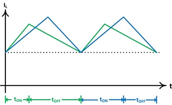
As an example, let’s assume that you needed to get 3.3 V out of a lithium-ion battery with a typical voltage range of 4.2 V to 2.8 V. If you used a buck converter, the battery cut-off voltage would need to be greater than 3.3 V, with the drawback of leaving energy stored in the battery unused. However, a buck-boost converter can help squeeze all of the energy out of the battery because it can also drain the energy stored when the input voltage is equal to or lower than 3.3 V, as visualized in Figure 2.

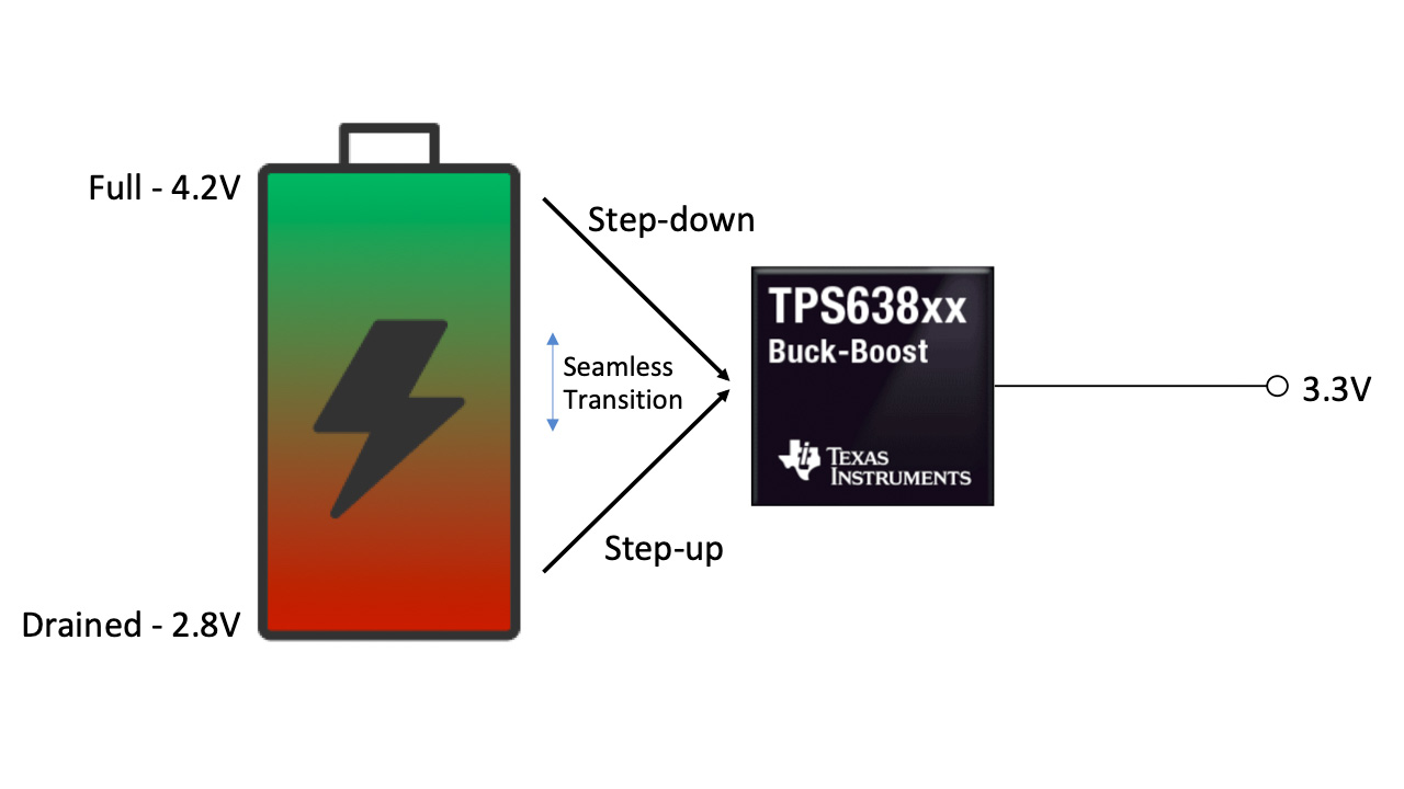
Figure 2: A buck-boost converter drains the battery completely


Using buck-boost converters as voltage stabilizers

A second common use for a buck-boost converter is as a voltage stabilizer. You’ll need a voltage-stabilizing buck-boost converter if a supply rail has variations (such as 3.3 V with ±10% variation) while the load requires a more precisely regulated voltage (such as 3.3 V with ±5% tolerance). A more tightly regulated voltage could be required if components are sensitive to the supply voltage (such as transimpedance amplifiers in optical modules); if other DC/DC pre-regulators are not regulating tightly enough in industrial applications; or if other components such as e-fuses, load switches or long cables in the power path add voltage variation as a function of the current. A boost or buck converter alone could not solve this problem – a buck-boost converter, however, would be able to regulate the varying input voltage to the required, tighter limits. Figure 3 shows the TPS63802 responding to a fast ±0.5 V/10 µs line transient with significantly less than ±0.1V output voltage under-/overshoot.

Figure 3: Line Transient Response for the TPS63802 at VI = VO = 3.3V, ΔVI = ±0.5V

Additional applications for buck-boost converters

There are additional reasons to choose a buck-boost converter over a buck or boost converter alone. One of those reasons includes power ORing. Imagine a device such as a baby monitor powered by a 5-V USB wall adapter or two AA primary cells ranging from 3 V (when new) down to 1.6 V (when the batteries are drained). Only a buck-boost converter can accept a wide input voltage range from 5 V (wall adapter) down to 1.6 V (depleted battery while the wall adapter is not connected) and still generate a 3.3-V rail for the system. Apart from the buck-boost converter, you would only need two external diodes to avoid cross-currents from the wall adapter to the battery and to switch seamlessly to the battery if the wall adapter gets unplugged.

Buck-boost converter limitations

When the input voltage is close to the output voltage, the internal control loops of the buck-boost converter are often designed to toggle constantly between buck and boost mode. This works acceptably, but has drawbacks: mode toggling might show a varying switching frequency, a higher output voltage ripple and more electromagnetic interference (EMI). As a secondary effect, efficiency could dip slightly at this point.

To avoid the effects of mode toggling, look for devices with a dedicated buck-boost mode that keeps the output voltage ripple low. One example is TI’s new TPS638xx family of buck-boost converters, where a dedicated buck-boost mode and hysteresis avoid toggling with an easy-to-filter noise spectrum and lower EMI.

Can a buck-boost device handle all types of voltage conversion?

Since a buck-boost converter “contains” a buck and a boost converter, you could use it for any DC/DC voltage conversion – so from that perspective, the answer is yes. But there are more details to consider. Table 1 provides an overview of given input voltage ranges vs. the required output voltage, and if a buck-, boost- or buck-boost converter is a good solution.


 Input/output voltage

 Boost converter

 Buck converter

 Buck-boost converter

 VIN always higher than VOUT

 Does not work

 Ideal topology

 Works, but possible drawbacks in efficiency (one additional integrated transistor with on-resistance present in the conducting path), solution size (more silicon area needed) and quiescent current consumption

 VIN always lower than VOUT

 Ideal topology, but needs a specific setup for disconnecting the battery from the load when disabled

 Does not work

 VIN higher or lower than VOUT

 Does not work

 Does not work

 Ideal topology

 Boost and buck converter in series: works, but drawbacks in efficiency,   solution size, passive component size and costs

Table 1: DC/DC conversion topology overview

Let’s return to the original question serving as the title of this article: Is there a universal tool for DC/DC voltage conversion? Not exactly. Analog designers working on high-volume products will prefer the performance optimization of a dedicated boost or buck converter when a buck-boost converter is not required. However, designers working on small-volume products may consider that some trade-offs are worth the convenience.

Using a buck-boost universally (to buck-boost, boost and buck) could provide these benefits:

  • Scaling across projects, to save time and mitigate design risks.
  • Reducing the number of different DC/DC converters to a narrow list of easy-to-use buck-boost converters.
  • Streamlining procurement, with a less complex inventory, larger volumes for price leveraging and supply stability.
  • Benefitting from the fact that a buck-boost disconnects the load from the supply during shutdown, while other topologies might need an additional load switch.

Additional resources


When to use rechargeable batteries in small battery applications

$
0
0

From starting a car to powering a television remote, batteries provide the power that makes everyday objects possible. Yet not all batteries are made equal. Some are rated for lower temperatures, while others can provide higher peak-current discharge rates. Choosing the right battery can reduce an end product’s size, prolong its useful life and make it more robust.

When developing a new blood glucose monitor battery specification, your most critical decision will be whether the battery chemistry is disposable or rechargeable. Primary cells are typically cheaper, more energy dense and simpler to use – but also bulkier, wasteful and prone to leakage. As seen in Figure 1 below, rechargeable cells are more customizable in their performance, have longer lifetimes, and enable a sleeker and more compact design.

Figure 1: Typical rechargeable battery

Rechargeable batteries are also typically more expensive and complex to implement because of the additional components required for their operation. To many designers, these drawbacks mean that primary cells are the only choice for applications like blood glucose monitors. But rechargeable solutions add more value than just environmental benefits, even for simple and inexpensive devices.

To start, since it’s not possible to recharge primary-cell batteries, any device like a handheld monitor that uses them as a power source must factor in how much power is drained per hour of usage in order to determine the capacity needed for useful device run times. Consumers don’t like replacing the batteries on their devices daily or even weekly, so the capacity requirement must be many times the daily consumption.

To illustrate this fact, imagine that you’re designing a patch for monitoring posture at work. The device uses 50 mAh every eight hours at 4.2 V and has an intended 100 hours of use before replacement. To meet these performance targets with a primary cell, the capacity of the battery would have to be at least 625 mAh to provide enough power to the device. This unused capacity adds weight and size to a design that you could use elsewhere.

Meanwhile, a rechargeable battery would not need to last 100 hours; it only needs to power the worst case of use between charge cycles. If the device had 20 hours of use between rest periods, then you could design your system with a 125-mAh battery instead of the 625-mAh battery. Even though a primary-cell battery is three times as dense as its rechargeable alternative, this reduced capacity requirement more than compensates for the shortfall.

Another factor to consider with a primary-cell battery is battery content leakage, especially for alkaline-style batteries. As a battery is used, a chemical reaction occurs that can lead to an excess buildup of pressure within the cell. To cut costs, some primary-cell batteries are not made with the best venting or materials available. This leads to a structurally weak cell that over time can leak its contents onto sensitive electrodes, possibly damaging the affected device permanently. As a designer, why add another vector in which your device might fail?

Outside of the potential harm to the device, a primary-cell battery must be replaced semi-regularly. We have all had to change the battery in a remote after weeks of less-than-stellar signal strength. Once depleted, some primary cells require special disposal practices; all generate waste at higher rates than their rechargeable counterparts. As the world becomes more and more eco-conscious, you would be right to be concerned about the waste generated by millions of people replacing a battery every 100 hours vs. 2,000 hours of use, all because of your design choice.

Primary cells are at a steep disadvantage when dealing with growing energy consumption. Consumers like to be able to track their activity and other data through online applications. As things like Bluetooth® Low Energy and other communication standards are integrated into our everyday lives, energy demands increase and size decreases. Devices no longer sit idle when not in use but instead provide regular reports. This functionality expends energy, increasing the average energy per hour of use. Consumers will always want their devices to do more; rechargeable batteries enable that desire.

Chargers like the BQ25155 and the BQ25125 are small, simple to implement and powerful. With integrated low-dropout regulators, analog-to-digital and DC/DC converters, it is possible for these devices to be comprehensive battery-management units.

TI has a broad breadth of resources to guide you through the process of integrating a power-management system into your future designs, whether you’re an absolute novice or a power expert. From designs using 60-mAh batteries in your blood glucose monitors to the 5-Ah battery in your favorite power tool, we have a solution and support for any scenario.

Additional resources

Three ways to drive multiple displays in an integrated digital cockpit with FPD-Link III

$
0
0

One of the ways automakers are differentiating themselves is by providing more advanced infotainment systems, with some luxury models featuring as many as 10 to 15 display panels and more complex processing and functionality. At the other end of the spectrum, entry-level models are migrating toward a minimalist digital infotainment system that gives drivers a basic central information display (CID) and a digital cluster. There has also been an increased push to provide a fully functional infotainment system in entry-level vehicles that can still use a complex digital processor to drive multiple displays in a cost and space-efficient manner.

Central processing vs. distributed processing

A CID might display several types of video content: a feed from the backup camera when the car is in reverse, or content from an audio player or GPS/maps for navigation when the car is in drive.

The same CID console may be used as a primary human machine interface touch screen to tune an AM/FM radio, make a phone call or show diagnostic information related to the car. Data aggregated from sensor modules, telematics control units or diagnostic modules must be processed and displayed on the CID in a format that drivers can easily understand and read. The easiest way to process disparate information and display the data would be to use multiple processors driving multiple displays. While using multiple processors seems logical, it brings up two major issues:

  • An increase in complexity to develop software for two processors while ensuring that the information output from multiple processors is context-synchronized, allowing information displays to adjust based on the surrounding environment (such as time of day or the presence of road signs).
  • A significant increase in cost and space: multiple processors supporting larger head units means a corresponding increase in heat from the increased power dissipation.

These drawbacks are causing automakers to adopt more centralized processing architectures, using a single processor that can take in data from various modules and output data from multiple inputs and multiple interfaces, thus driving multiple displays. A single processor in a central processing application has the added benefit of being able to create augmented video images, like a synthesized image of the top view of the car based on an aggregation of images from various sensors placed around a vehicle.

Driving multiple displays from a single processor in a head unit

What does it take to drive multiple displays from a single processor? The vehicle processing unit is physically separated from the display panels with which the unit is interfacing. Adding to this complexity, the electrical interface going into a display panel could be completely different from the electrical output interface coming out of the processor.

This is where our FPD-Link interface devices come into play. These serializers and deserializers (SerDes) bridge processor output interfaces to display input interfaces in order to provide seamless connections. In addition to bridging, these devices enable the aggregation of data from various protocols coming out of a processor into a single or dual pair of wires and also provide a backchannel for simultaneous data transfer, like touch control data from display panels back to the vehicle processing unit.

The DS90UB941AS-Q1 is an FPD-Link III serializer that can interface to a processor using a single/dual Display Serial Interface (DSI). When used in combination with an FPD-Link III deserializer, this device can bridge between DSI and a display interface like OpenLDI or an RGB interface.

Using this FPD-Link III product family, I’ll show you how to use a single processor to drive multiple displays in three different ways.

Using the multiple DSIs

In this method, the processor uses two separate DSI ports to drive two different video streams into two displays. The DS90UB941AS-Q1 supports two independent DSI ports, so using one of these devices; a processor can drive two different 720p video streams into two displays, like a CID and a cluster. The device can support two independent DSI streams and act like two independent serializers in this mode, as shown in Figure 1.


Figure 1: Using two independent DSIs to drive two displays

Using the virtual channel feature

In this method, the processor uses a single DSI port connected to the DS90UB941AS-Q1, but uses its Mobile Industry Processor Interface DSI virtual-channel-based splitting feature. This device can split images based on the DSI virtual-channel ID. In this mode, a single DSI input can include two different video streams delineated by the virtual-channel ID, as shown in Figure 2.


Figure 2: DSI virtual-channel-based video splitting to drive two displays

Using the superframe support feature

In this method, the processor uses a single DSI port to drive two different video streams into two displays. This method harnesses two powerful features of the DS90UB941AS-Q1: super-frame support and symmetrical/asymmetrical splitting.

A superframe, as the name implies, is made of two or more video streams that are combined in a specific way. Figure 3 is an example of an asymmetrical superframe.

Figure 3: Superframe-based asymmetrical video splitting to drive two displays

A superframe generated from a combination of multiple video streams by the external processor system-on-chip can then pass into the DS90UB941AS-Q1 as a single video stream. This device can process this combined video stream, asymmetrically split the video streams and ship each video stream to two different displays.

Knowing how to interface to multiple display panels using a single processor will help you reduce cost and complexity in your next-generation automotive infotainment system. For more information on superframes and symmetrical/asymmetrical splitting, check out the application report, “Splitter Mode Operations with the DS90UB941AS-Q1.”

Designing smarter remote terminal units for microgrids

$
0
0
Microgrids are becoming a popular solution for increasing the availability of power and optimizing energy costs. In remote areas, microgrids take the place of traditional power grids by using renewable energy, like solar or wind power. In areas with a...(read more)

Designing a building security system with the Sub-1 GHz Linux Gateway Software Development Kit

$
0
0

Building security systems come in many system topologies, ranging from a simple alarm system to a complicated network of sensors that all report to a main security panel acting as a hub. These systems are either wired or wireless based on their deployment, and when wireless leverage many different types of connectivity to achieve their specific application. Some applications (like security cameras) use Wi-Fi® for a native connection to the cloud, while some smart applications (like door locks) use Bluetooth® low energy in order to connect to phones and tablets. Security systems based on sensor networks, such as smoke detectors, motion detectors, door/window sensors, temp / humidity sensors, and glass-break detectors, can benefit from using Sub-1 GHz networks.

Sub-1 GHz technology offers many advantages when designing a building security system, including achieving much longer range and better wall penetration than 2.4 GHz technology. This enables whole building coverage without the need for repeaters and without having to use a complicated mesh network topology. Sub-1 GHz is also very low power, enabling remote sensors to operate for 10 years on a coin-cell battery. This benefit offers system design flexibility, eliminating the need to route wires inside ceilings and walls.

One essential point when designing building security systems is that the communication must be reliable. Sub-1 GHz systems offer high robustness by taking advantage of the Sub-1 GHz frequency band, which is less crowded than the 2.4 GHZ band.

While it is clear that Sub-1 GHz has many key advantages for building security design, often security systems and sensors must have a cloud connection or a smart device interface requiring Wi-Fi and Bluetooth low energy. However, it is very complicated to design a system that sends and receives sensor data over a Sub-1 GHz star network, connects to the cloud, and provides a smart device interface. Thanks to the dual-band capabilities and flexible radio features of the CC1352P wireless microcontroller (MCU) and the Sub-1 GHz Linux Gateway solution, you can easily develop products that seamlessly connect to both smart devices and the cloud while still leveraging the benefits of Sub-1 GHz technology with an integrated, low power 20dBm PA for longer range.

The Sub-1 GHz Linux Gateway SDKscales to many different applications. For instance, imagine designing a building security system including smoke detectorsmotion detectorsdoor & window sensors, and glass-break detectors covering a whole building, and all communicating with a centralized security panel. The system design requires that consumers view sensor data on the web or a smart device. The solution can help achieve this use case, while supporting a fast time to market and being flexible enough to enable various solution architectures.

Figure 1: Home security system example

As Figure 1 shows, the peripheral sensors (smoke detector, motion detector, door/window sensors and glass-break detectors) all talk to the central security panel over a Sub-1 GHz star network. The security system leverages the long range and wall penetration of Sub-1 GHz to cover the whole building. Additionally, you can place sensors that don’t have access to AC power, like the door and window sensors, remotely; they can run for 10 years on a coin-cell battery. Using the CC13152P dual-band MCU, the smoke detector can connect over Bluetooth low energy to a phone or tablet and send users alerts on their smart device.

These alerts can report battery life or any danger detected, while the smoke detectors communicate to the main security panel over the Sub-1 GHz network. The security panel can collect data from all of the sensors and, using Wi-Fi, connect to the cloud to report to the security company or enable visualization of the data on the web. Users can also update the system firmware by connecting to the panel with Bluetooth low energy or receiving the updates from the cloud. The panel can then push those updates out to the peripherals and update the firmware of each node over the Sub-1 GHz network.

This building security system example is just one use case enabled by TI’s Sub-1 GHz gateway solution. The gateway architecture is flexible, enabling interfaces to multiple cloud providers andthe design is based on proven hardware and software from the SimpleLink MCU platform, which will shorten development time and enable quick time to market. Take advantage of the solution and start your design today.

Additional resources

Space Enhanced Plastic gives designers a new solution for emerging low-Earth orbit commercial applications

$
0
0
One of the more exciting aspects of the emerging new space market is the launch of high-volume low-Earth-orbit (LEO) satellites that are small and economically feasible, but also radiation-tolerant and reliable. These satellites enable expanded communication...(read more)

Ethernet-based control and monitoring of Vienna rectifiers using the latest addition to the C2000 MCU family

$
0
0
Chen Jiang co-authored this technical article. Automakers are starting to invest heavily in electric vehicles (EVs), with the market expected to grow from around 3 million units in 2019 to 27 million units by 2030; that’s a 21.1% compound annual...(read more)

Powering infotainment systems of the future

$
0
0

Everywhere you turn, you hear about “cars of the future.” As the automotive industry continues to make leaps with autonomous vehicles, what will the driving experience be like when people no longer have to actively drive the car?

That is no longer a hypothetical question. As our attention will no longer be directed at operating the vehicle, in-vehicle entertainment will become far more important. Ever-more-impressive infotainment systems already allow the drivers as well as the passengers to gather important information about their car and journey, while also being entertained, and this trend will only continue to accelerate.

Judging from concept cars showcased at auto shows around the world, these infotainment systems will no longer be contained to solely the center console but will instead stretch across the entire dashboard (see Figure 1) while also including screens on the steering wheel, the backs of front-seat headrests, and even on the windshield with head-up displays, which allow drivers to see directions and other crucial information without taking their eyes off the road.

Figure 1: Example of a future Infotainment system (Digital Cockpit) that spans much of the dashboard

These ever-more-complex systems will provide drivers and passengers with an incredible assortment of benefits in the Head Unit or Integrated Cockpit such as navigation, car diagnostic information, wireless and Bluetooth® connectivity, music selection, and video entertainment. All of these functions will require significant data processing. Additionally, the screens used to display this information will not only increase in number and size, but also in resolution, thus requiring more power.

Today, infotainment systems that run off of a car battery typically use 3 A to 4 A to supply power to the processor and displays. This is sufficient for powering only one display; this power level can also sufficiently support the processor. But larger, more numerous displays increase the power requirements accordingly, with many systems requiring 6 A of current off the battery and some elaborate systems requiring 8 A to 10 A.

As a result, engineers need to look for DC/DC buck converter and controller products that offer the power, electromagnetic interference (EMI) performance and efficiency that these types of applications require. With infotainment systems operating off of car batteries, it will become increasingly important to use high-efficiency power solutions to minimize the amount of heat put out by the system, while also ensuring that the battery doesn’t dissipate heat excessively when the car is off.

The LM5143-Q1 is one example of a device that addresses these issues. This low quiescent current two-phase controller can easily support the 8- to 10-A output currents seen in the newest infotainment systems. Given the thermal challenges that arise at these higher output currents, the LM5143-Q1 and its external field-effect transistors offer an appealing solution due to their additional flexibility. Alternatively, the LM61460-Q1 offers a peak efficiency of over 93% at common-load currents (see Figure 2) minimizing thermal dissipation and allowing you to focus on other aspects of your design. The device’s good EMI performance, a key priority for infotainment systems, helps minimize the amount of noise present near the FM radio (leading to audible noise), as well as near other systems where EMI can affect proper operation.

Figure 2: Efficiency for the LM61460-Q1

The future is very exciting for the infotainment market, with boundless potential. That being said, high-powered infotainment systems also present unique challenges such as thermal dissipation and the need for a reduced total solution size. The LM5143-Q1 and LM61460-Q1 DC/DC solutions can help with these challenges and address the increasing need for higher-current buck converters.

Additional resources


Concerned about transitioning from Class-AB to a Class-D? Well, you shouldn’t be.

$
0
0

Have you ever dreamed of doing something awesome but psyched yourself out, thinking that it was going to be too hard to complete? Then, after you finally got the courage to go for it, you looked back in astonishment – it was really fairly easy.

This is the scenario I’m witnessing lately when speaking with automotive audio design engineers about switching their car radio solution from a traditional Class-AB amplifier to a Class-D amplifier. So let’s talk about the two primary concerns that I hear about most often: the impact on printed circuit board (PCB) size and potential electromagnetic interference (EMI) concerns.

Concern No. 1: Class-D amplifiers are going to enlarge your PCB footprint

Typical Class-D audio amplifiers switch the amplifier on and off at ~400 kHz and require the use of 8.2-µH or 10-µH inductors for proper audio performance.

TI’s TPA6304-Q1 Class-D amplifier switches at a 2.1-MHz switching frequency. It’s reduced ripple current means that it can take advantage of much smaller and lighter-weight 3.3-µH inductors, as shown in Figure 1.

Figure 1: Comparison of inductor size vs. switching frequency

The TPA6304-Q1 is designed with TI’s latest mixed-signal manufacturing technology, which when coupled with the use of 3.3-µH Inductors shrinks the overall size of the complete four-channel amplifier solution (including all required passive components) to 272 mm2, as shown in Figure 2.

Figure 2: The TPA6304-Q1 four-channel Class-D amplifier

To put this into perspective, Figure 3 shows that the complete TPA6304-Q1 solution is smaller than a traditional Class-AB amplifier by itself.

Figure 3: TPA6304-Q1 Class-D amplifier solution size compared to a Class-AB amplifier

Concern No. 2: Class-D amplifiers introduce EMC issues

By nature, a Class-D audio amplifier switches its output on and off during each cycle of the clock, whereas a Class-AB amplifier does not switch. This does not imply, however, that a Class-D amplifier will introduce unmanageable electromagnetic compatibility (EMC) issues.

I’d like to specifically review several ways that the TPA6304-Q1’s amplifier design helps alleviate EMC concerns:

  • The TPA6304-Q1 device design is highly optimized to manage overall EMC behavior. Also, the 3.3-µH inductors discussed previously are part of the inductor-capacitor (LC) filter, which helps minimize EMC from the high-speed switching transients on the output stages of Class-D amplifiers.
  • Traditional Class-D amplifiers that switch in the 400-kHz range create harmonics that lay directly within the AM band, as shown in Figure 4. These harmonics create interfering signals that reduce AM receiver sensitivity, thereby hindering AM radio station reception. Therefore, some type of EMI avoidance scheme must be implemented on these 400-kHz Class-D amplifier designs to mitigate the effects of these AM band harmonics.

Figure 4: Typical 400-kHz Class-D amplifier harmonics

  • By operating at a much higher 2.1-MHz switching frequency, the TPA6304-Q1 eliminates the need to implement an EMI avoidance scheme for the AM band because the TPA6304-Q1 amplifier provides significant margin above the AM band. This design is also free of any lower-frequency spikes that would interfere in the AM band, as shown in Figure 5.

Figure 5: The TPA6304-Q1’s high switching frequency above the AM band

In case some PCB layout designs introduce EMI challenges, the TPA6304-Q1 has implemented a Kilby Labs-developed, proprietary spread-spectrum technique. Figure 6 illustrates how this feature helps spread out a narrowband energy source across a much larger frequency band, thereby reducing the peak energy.

Figure 6: Spread-spectrum technology background

Conclusion

The TPA6304-Q1 2.1-MHz higher-switching-frequency automotive Class-D audio amplifier fulfills industry demands for next-generation car radios and external amplifiers. In addition to reducing the thermal load in systems, the amplifier’s design addresses concerns about PCB size and EMC when transitioning from Class-AB amplifiers to Class-D amplifiers.

Additional resources

How to enable thermal safety for automotive infotainment and cluster systems

$
0
0

Next-generation cars now come equipped with ever-more-complex infotainment and cluster systems. But the increased electronic content in modern vehicles consumes more energy, which generates more heat. Car dashboards are already exposed to solar loading and high temperatures as a result of cabin heating.

Due to the increased heat throughout infotainment and cluster systems, automakers must now overcome new thermal-management challenges. They need to offer a feature-rich and comfortable driving experience that appeals to customers while ensuring safe and reliable operation of the crucial functions these systems provide – all within a limited budget.

Figure 1 identifies various infotainment and cluster applications, each with their respective thermal problems.

Figure 1: Infotainment and cluster systems where thermal issues are a key concern

Securing overloaded microprocessors in automotive head units

Automotive head units have become the main control panel for infotainment systems, aggregating many different functions that were formerly dispersed throughout the car, serviced with various buttons. Such centralization makes this head unit the brain of the infotainment system, featuring important processing power via application processors that tend to heat up fast as the processing load increases.

The majority of heat generation and risk comes from the core of these microprocessors. To get the most reliable temperature measurement, it’s common to sense remotely via a P-N junction whether it’s a substrate thermal transistor or diode in the die of the processor.

TI designed the TMP451-Q1 for these remote sensing cases, with a ±1°C typical accuracy from -40°C to 125°C, for either the remote channel (the processor core) or locally (where the temperature sensor is placed), providing two temperature readings to the system. To limit the power consumption and thus self-heating that impacts temperature accuracy, the TMP451-Q1 operates with a low 1.7-V to 3.6-V power supply, consuming only 27 µA of operating current while making 0.0625 conversions per second.

The TMP451-Q1 is also well-suited to space-constrained head-unit PCB boards, thanks to its 8-pin, 2-mm-by-2-mm very very thin small outline no-lead package. There is a 2.5-mm-by-2.5-mm wettable flank version of this package as well that complies with the automatic optical inspection (AOI) process found in the automotive industry for fast solder verification on the electronic board.

The device has alert functions that serve as interrupts to modify system behavior when the temperature rises above a specific threshold. Two alert functions, THERM and ALERT/THERM2, provide more control of system thermal management.

As shown in Figure 2, setting a first interrupt (THERM2) to 85°C as a warning can trigger a fan, a cooling system or decrease the performance of the microprocessor to reduce the risk of overheating. The second interrupt (THERM), at 110°C, would actually shut down the system to save it from being damaged. For example, it could order the power supply to shut down and start a system reset until the temperature goes below the THERM hysteresis level.

Figure 2: The THERM and THERM2 interrupt operations in the TMP451-Q1

Measuring system temperature accurately in reconfigurable clusters

Automotive instrument clusters provide crucial information such as speed, RPMs, fuel levels and oil temperature gauges – information that will affect a driver’s decision-making.

But today, similar to the digitalization of head units, instrument clusters are being upgraded to reconfigurable clusters. These reconfigurable clusters provide a personalized display with navigation, media, contacts and more. This can be very demanding on the microprocessor, which automatically heats up with increasing processing needs, especially since ventilation is usually nonexistent given the very limited space behind the steering wheel.

To obtain relevant temperature measurements, it is possible to place very small temperature sensors close to the microprocessor, which will help with reading accuracy. With a highly accurate reading, you can push the performance of the system closer to its thermal design limits or reduce system costs by choosing a microprocessor with lower specifications.

Indeed, while most processors have built-in temperature sensors, because of variations across wafers and other various lots, accuracy is only consistent at ±4°C. With such variance in the reading accuracy, you must account for a broader safety margin than one with a reading of ±1°C accuracy. In this case, the microprocessor would have 3°C of extra performance room without coming too close to the thermal design limit (see Figure 3).

Figure 3: Enhancing system performance through high-accuracy thermal monitoring

The TMP235-Q1 boasts ±0.5°C accuracy from -40°C to 150°C (Grade 0). The device has a very small footprint (2.00 mm by 1.25 mm – see Figure 4) and low power consumption.


Figure 4: The TMP235-Q1 analog temperature sensor

Protecting systems and USB chargers from thermal damage

New USB chargers not only support USB Type A, but now USB Type-C™, which often includes power delivery capabilities from 60 W to 100 W. If you have multiple ports this wattage is multiplied, heating up dangerously and can potentially be hazardous. USB controller integrated circuits (ICs) typically have programmable cable droop compensation to help portable devices charge at an optimal current and voltage under heavy loads. Implementing a thermistor for intelligent thermal management can give an indication of the temperature to USB controllers and make them change their output current limit to lower levels in order to decrease the temperature.

The TMP61-Q1, for example, is a thermistor with a positive thermal coefficient, providing a linear output in a very small package: 1 mm by 0.5 mm.

Temperature switches can also protect systems against overtemperatures by sending an alert to the USB controller IC when the temperature crosses a certain threshold set by resistors, voltage or factory-programmed. This alert can bypass the microcontroller (MCU) to take a quicker, more direct decision. Depending on the temperature threshold, the MCU could also fail at lower temperatures than the temperature sensor. So there needs to be a protective system that can shut down this noncritical functionality of the car for passenger safety and to avoid thermal runaway. Furthermore, using a temperature switch is cost-competitive in comparison to a discrete implementation (Figure 5) because there’s no need to have extra circuitry like comparators and voltage references to detect the threshold.


Figure 5: Discrete implementation of a temperature switch

The TMP390-Q1 resistor programmable temperature switch covers the -40°C to +125°C temperature range with a ±3.0°C maximum accuracy. It has two channels that enable independent overtemperature (hot) and undertemperature (cold) detection simultaneously (see Figure 6). The TMP390-Q1 is also a low-power-consumption alternative to the thermistor, as it can be supplied with power from 1.62 to 5.5 V and consumes 0.5 µA at 25°C. The device offers the simplest thermal protection implementation and is also the most integrated as it includes a protection from both cold and heat in one chip.


Figure 6: Undertemperature and Overtemperature protection with the TMP390-Q1

There are various ways to deal with temperature monitoring and protection in infotainment systems, and many other aspects to consider. With the increasing number of features and displays in cars that are increasing the processing demands, ensuring thermal safety is critical in order to avoid accidents.

Additional resources

Making a connection with smart meters

$
0
0

Grid infrastructure often plays a pivotal role in the success or failure of any modern economy, since electricity, water and gas resources are essential in powering commerce and industry. So that utility companies and municipalities can get the most from their infrastructure investment, they use smart metering technologies to enhance grid resource efficiency and facilitate more accurate billing, fault monitoring and faster provisioning of services. In addition, for deregulated markets, smart meters allow utilities to offer unique services and promotions, leading to healthy competition among vendors.

Smart meters can incorporate many different capabilities, but their ability to wirelessly send and receive information is arguably the most important. Wireless connectivity enables smart meters to not only send metering data to utility companies but to respond to commands from utility companies, turning a group of individual meters into a dynamic network.

Given the importance of connectivity, the implementation of a wireless connectivity function within a smart meter is often a concern. Today, many smart meter designs use special communication modules designed for specific communication standards such as 2G-General Packet Radio Service, 3G, 4G-Long-Term Evolution and low-power wide-area, as well as shorter-range standards such as Wi-Fi® and Bluetooth®. Figure 1 shows an example of a modern smart electric meter.

Figure 1: Reference diagram for a smart electric meter

One challenge that designers face when incorporating communication modules into their design is interfacing the module with the meter’s existing processor control and data input/output (I/O). Often, the components incorporated into the module are designed in different silicon process technologies, thus requiring the modules to operate on voltage nodes different than the nodes used by mainstream microcontrollers and processors.

In order to overcome the challenges posed by I/O voltage-level mismatches between a meter’s main processor and a communications module, you can use simple building-block devices like voltage-level translators. Voltage-level translators enable you to quickly and cost-effectively level shift the control and data interfaces between the module and the processor so that the two devices can interoperate.

Level translators are available in wide variety of configurations, covering channel counts from one to 32 channels with support for voltage levels from 0.65 V to 5.5 V. Level-translator devices can be used to level shift interface standards such as Serial Peripheral Interface (SPI), I2C and Universal Asynchronous Receiver Transmitter (UART), as well as general-purpose I/O (GPIO) for more custom implementations. Let’s take a look at a few examples of level shifting for some of these interface types.

If the interface between a communications module and the meter’s processor is SPI, a device like the SN74AXC4T774 level translator can provide an efficient and easy way to implement a level-translation solution, as shown in Figure 2. This device’s per-channel direction control capability makes it a good fit for SPI, where not all of the channels of the interface are operating in the same direction.

Figure 2: SPI level-translation example using the SN74AXC4T774

Another common control interface between a communication module and a smart meter’s microcontroller is I2C. I2C control buses are popular open-drain control buses implemented in many systems. Often, the controller will operate on a common voltage node such as 3.3 V with a 3.3-V I2C control bus, while the communications module will operate at a lower voltage such as 1.8 V with a 1.8-V or lower-voltage I/O. In this case, an auto-directional level translator such as the LSF0102 can level shift between the 1.8-V I2C I/O of the communications module and the 3.3-V I2C control bus, as shown in Figure 3.

Figure 3: I2C control bus level-translation example using the LSF0102

Similarly, you can level shift GPIO, as shown in Figure 4. The SN74AXC2T45 is a direction controlled level shifter which provides flexibility needed for GPIO implementations.

Figure 4: GPIO level-translation example using the SN74AXC2T45

As smart metering technology evolves, level-translation solutions from TI can enable smart meter designers to implement critical connectivity between subsystems within their designs.

Additional resources

Taking the family-first approach to op amp design

$
0
0

The first time I visited a Texas barbecue restaurant, I was astounded by all the different types of meat on the menu and couldn’t decide what I wanted. Luckily, the restaurant offered a three-meat plate so that I could try a sample of the options.

As a design engineer looking for an operational amplifier (op amp), you also have a plethora of options. Plus, with the aggressive timelines of today’s production cycles, you need to make a decision fast. Choosing the wrong op amp for the job can cost time and money.

TI’s versatile op amp portfolio comprises 48 unique amplifiers, including the new TLV9001, TLV9052, TLV9064, offered across 16 different packages, including the industry’s smallest single- and quad-channel packages. In this technical article, you’ll learn how this new op amp family fits a variety of project needs, enabling reduced printed circuit board (PCB) space and offering versatile bandwidth options to provide more gain for your signal chain.

With the largest op amp portfolio on the market, you can choose the exact channel count, speed and size your system needs.

Design versatility through performance

Figure 1 outlines the full device family, with similarities highlighted at the top. The three subfamilies are interchangeable because they use the same supply voltage, input and output voltage range, and offset voltage. Additionally, their similar low, resistive output impedances minimize stability issues.

Figure 1: Amplifier family comparison

Each subfamily provides unique performance benefits, however. For example, if you initially used the TLV9002 in a single-supply low-side, unidirectional current-sensing solution with output swing to GND circuit for motor current sensing, but later determined that a higher gain and a faster slew rate were required in order to handle large motor-current transients, you could easily switch to the higher-bandwidth, pin-to-pin-compatible TLV9052 without a major redesign effort. This is possible because each subfamily is offered in the same 16 package options, covering all three channel configurations.

Package flexibility

Figure 2 lists the details of each package option. The Industry Standard column determines whether the package is available from other suppliers for second-sourcing options. The Shutdown column highlights which packages feature shutdown functionality, which helps reduce overall power consumption.

While the majority of the small package options are quad flat no-lead (QFN) packages, I want to highlight one that is not. The dual-channel, small-outline transistor (SOT)-23-THIN package uses the body of a single-channel SOT-23 package but has eight pins instead of the traditional five or six pins. This can be a great alternative to the much larger leaded packages such as small-outline integrated circuit (SOIC), thin-shrink small-outline package (TSSOP), or very-thin-shrink small-outline package (VSSOP). It’s also possible to use a dual-layout technique in order to multi-source an eight-pin SOT-23 and a traditional leaded package. The Analog Design Journal article, “Second-sourcing options for small-package amplifiers,” provides additional details. However, I recommend reviewing the QFN options if you are trying to minimize PCB space.

Figure 2: Amplifier family package options

Size breakthroughs

These three amplifier sub-families feature the industry’s smallest single-and quad-channel packages. Compared to competing small-size devices, TI’s single-channel 0.8-mm-by-0.8-mm extra-small-outline no-lead (X2SON) package is 13% smaller, while its 2.0-mm-by-2.0mm extra-small QFN (X2QFN) package is 7% smaller. These packages along with the dual-channel 1.0-mm-by-1.5mm X2QFN package, give you multiple options to help reduce PCB area. You can see all three packages along the right side of Figure 3.

Figure 3: The road to smaller packages

Because manufacturing technologies can limit the use of ultra-small QFN packaging due to a small pin pitch, TI also offers multiple small package options, with varying pin pitch. The application report, “Designing and Manufacturing with TI’s X2SON Packages” provides layout and routing guidance when it comes to these packages.

Wrapping up

Some say that too many options can lead to choice paralysis. I say that, whether you’re in Texas trying to decide what barbecue you want or a design engineer trying to choose an amp, the more options the better. The next time you’re starting a design, plan choose an op amp family that that lets you pick from three different performance levels and, one of 16 unique package options, and save PCB area when you need it with the industry’s smallest single-and quad-channel packages.

Additional resources

  1. Evaluate eight of the small package options by ordering the small amplifier dual inline package evaluation module.
  2. See a detailed comparison between the TLV9002, TLV9052, and TLV9062 specifications.
  3. Simulate designs using the TLV9002, TLV9052 and TLV9062 TINA-TI™ software Spice models.
  4. Explore the world’s largest amplifier portfolio.

Build smarter factories with TI’s ultrasonic sensors

$
0
0

A key driver of efficiency within a factory is automation; more and more factories are starting to adopt a factory environment that is fully autonomous, known as “lights-out manufacturing.” Sensors are a key component of the intelligence required to achieve this level of automation.

TI has created an animated video that showcases six examples of ultrasonic sensing to kick-start the world of automation:

(Please visit the site to view this video)

The six examples are:

  • Drone collision avoidance sensors. Already popular in the consumer and medical spaces, drones are finding uses in the industrial space for aerial photography. Industrial companies are also looking at drones to deliver packages from facilities to homes or from one spot in a large factory to another. Ultrasonic sensors in such applications sense for any obstacles so that the drone can steer its course. A benefit of using ultrasonic technology is its ability to work in any ambient lighting conditions and to detect clear surfaces like windows and water.
  • Automated door and gate sensors. Found nearly everywhere – supermarkets, offices, parking garages and large warehouses – automated doors and gates offer a hands-free method to enter buildings. It is important to be able to detect humans or vehicles approaching a door but ignore smaller objects like debris or small animals. Ultrasonic sensors work even in the presence of rain and fog and are more reliable than infrared-based solutions.
  • Occupancy detection sensors. Buildings and factories use occupancy sensors to lower energy consumption and improve security. Energy control is driven by the increasing integration of electronics and network capabilities, along with power-consumption limits adopted in some countries. Occupancy sensors can detect people in conference rooms, detect whether people are present in a “caution” zone in large open spaces, or wake appliances up from sleep mode when a user approaches. While passive-infrared (PIR) sensors are the cheapest sensors, they can be unreliable and lead to false positive readings. Ultrasonic sensors, used either in addition to PIR or stand-alone, can provide more confident sensor readings.
  • Industrial robot sensors. Robotic arms are found all around manufacturing and assembly lines in factories to fabricate material or look for defects. Sensors integrated in industrial robots need to be flexible and adjustable in case there is a change in the manufacturing process or end product. For example, in a soda factory, sensors mounted at the head of the liquid dispenser ensure that the soda bottle is face up and aligned to prevent liquids from spilling. Ultrasonic transducers come in many frequencies (enabling flexibilities in resolution and range), and the technology itself can detect clear objects, which proves advantageous in industrial robotic applications.
  • Logistic robot sensors. Some warehouse robots transport packages from one end of a factory to another. Sensors mounted on robots help them maneuver through factory floors without colliding into walls, objects or humans. Ultrasonic sensors can detect up to 10 m, with a resolution of 1 cm or lower.
  • Level transmitters. In the food and drug industry, contactless level transmitters avoid product contamination. Ultrasonic is one of the most reliable contactless sensing technologies for use inside containers and storage tanks compared to technologies like optical or infrared, due to the ability to detect clear liquids. Ultrasonic sensors can be mounted above, inside or underneath tanks to detect fluid levels and control the inflow and outflow of contents.

Ultrasonic sensors are a reliable choice for proximity-, position- and level-sensing applications due to their ability to reliably detect clear surfaces such as water and glass and to operate in adverse environments such as smoke, fog or rain.

Additional resources

Enabling smart meter wireless connectivity with level translation

$
0
0
Grid infrastructure often plays a pivotal role in the success or failure of any modern economy, since electricity, water and gas resources are essential in powering commerce and industry. So that utility companies and municipalities can get the most from...(read more)

How semiconductor technologies are changing automotive lighting roadmaps

$
0
0

Adaptive headlight systems | Animated rear lights | Personalized interior lighting | Brighter, customized puddle lights

 Automotive lighting from front to rear

Automotive lighting continues to evolve at breakneck speeds. While LED light sources have enabled efficiency improvements and unique vehicle styles, original equipment manufacturers (OEMs) are now implementing novel and beneficial lighting use cases. In this technical article, I’d like to highlight several semiconductor technologies that are impacting headlight, rear light and interior light system roadmaps.

Adaptive headlight systems

Adaptive front light systems and adaptive driving beam headlight systems adjust the shape of low and high beams, respectively. Although adaptive headlights are available on cars in Europe, automobile manufacturers in the U.S. cannot use these advanced lights, but this may change soon. These adaptive systems use high-powered LEDs as a light source, which requires high-powered LED drivers to regulate current and achieve the required brightness. Switching LED drivers must be used to achieve high efficiency and implemented as dual-stage power-processing topologies for thermal management.

The first stage is a boost voltage regulator, which manages the widely varying automotive input voltage and creates a stable intermediate rail. The second stage is a buck current regulator, which can be implemented with a low output capacitance suitable for dynamic LED loads. But because the LED drivers are implemented as switching regulators, you will have to address electromagnetic compatibility (EMC) challenges.

LED driver and matrix manager functionality and options

Given how quickly headlight systems are advancing, design flexibility is key. In adaptive systems, you can use the new TPS92682-Q1 dual-channel, dual-phase LED controller as a constant voltage boost regulator for the headlight’s first stage. If static headlights are on your roadmap, you can configure this device as a constant-current buck-boost/boost/single-ended primary-inductor converter (SEPIC) LED driver. The TPS92682-Q1 also has programmable spread-spectrum modulation that helps meet EMC requirements easily.

For the buck current regulator second stage, another device, the TPS92520-Q1, offers high power density in a small solution size, enabled through a monolithic, dual synchronous buck constant-current LED driver with up to 2.2-MHz switching frequency and Serial Peripheral Interface. In addition to the high level of integration and power density offered by the TPS92520-Q1, its control architecture provides true average current regulation, along with dynamic and matrix load compatibility.

While the TPS92682-Q1 and TPS92520-Q1 can be the driving forces of a headlight’s electronic control unit (ECU), found in any headlight system, it is the matrix-manager integrated circuits that are responsible for adjusting the headlight’s beam shape. Matrix managers are found in the headlight’s pixel board, where they precisely control the intensity of each pixel to generate different beam patterns and illuminate the entire field of view while avoiding glare from oncoming traffic.

Because LED pixel boards are typically cabled through a wire harness to the ECU, robust communication and reduced harness size are challenges. The TPS9266X-Q1 provides a robust yet lightweight communications interface as well as a full suite of diagnostics to detect and report pixel-level LED faults directly to the ECU.


Headlight ECU reference design 

 See how our two new LED drivers enable a complete 120-W matrix-compatible ECU for adaptive headlights.

DLP® technology functionality and options

TI DLP technology-based headlights not only enable high-resolution adjustment of headlight beam shapes; they also enable symbol projection to assist drivers. Symbols can communicate to both drivers as well as others on the road. For example, lane marking, which uses headlights to draw the planned path of the car on the road, can help drivers as they navigate hazardous driving conditions, and also help communicate to others where the vehicle will be traveling. The DLP5531-Q1 chipset is automotive-qualified, optimized for headlight applications and on the road today. Check out the DLP auto headlight reference design.

Motor functionality and options

Another way to change the light beam is headlight leveling, in which the beam lights the road regardless of the road inclination or whether the driver accelerates or decelerates. Pointing the headlight to the road especially enhances visibility while driving in the night making driving safer. Bipolar stepper motors are typically used to control headlight leveling. The DRV8899-Q1 stepper motor driver not only has the power stage to drive the motor, but also has stall detection capability without the need for an additional sensor. 

With the continued expansion of communication-based light control modules, TI’s portfolio of Controller Area Network (CAN) transceivers such as the TCAN1044-Q1, Local Interconnect Network (LIN) transceivers such as the TLIN1029-Q1, and system-basis chips such as the TCAN4550-Q1 and TLIN14415-Q1 are good options for automotive lighting applications.

Animated rear lights

LED light sources are becoming popular for rear light signal functionality such as brake lights and turn indicators, and can now even include animation and/or personalized lighting messages.

Static lighting

The Automotive Dual Stage (SEPIC + Linear) Static LED Driver Module Reference Design for Rear Lights shows a dual-stage LED driver with the first-stage voltage regulator implemented using the LM5155-Q1 configured in a SEPIC topology. This buck-boost topology enables operation of the lights at low battery voltages and regulates the voltage down at high battery voltages in order to optimize the second-stage LED drivers from a thermal management perspective.

Animated lighting

TI’s new 12-channel high-side LED driver, the TPS929120-Q1, was created for animated lighting applications. This device uses FlexWire, an interface unique to TI, to enable individual pixel control. FlexWire is a Universal Asynchronous Receiver Transmitter-based (UART) interface with automatic baud rate detection so that high-LED-count systems can dim independently. Full diagnostics and a fail-safe mode ensure reliability for full LED lamps.

The TPS929120-Q1 includes 12-bit pulse-width modulation (PWM) dimming and offers off-board support – suitable for rear lighting implementations that may span across the entire length of the vehicle, as shown in Figure 1. The TPS929120-Q1 can interface with CAN or LIN communication transceivers, as shown in the digital interface LED driving module reference design, for improved communication robustness.

Rear lighting that spans across the length of a vehicle

Figure 1: Rear lighting that spans across the length of a vehicle

Additional rear lighting trends

Rear lights are implementing new ways of signaling that combine styling and personalization. One example is the swiping turn, where the turn indicator LEDs light up in sequence instead of all at once, making it appear as if the turn indicator is swiping. Another trend is to use the rear light to display welcome messages for drivers or to even display message alerts for drivers behind the car.

Personalized interior lighting

Lighting inside the cabin is also changing. One such change is the adoption of a large array of LEDs in order to either display personal messages such as welcome messages or to adapt the light beam to shine at a specific location, such as on the front passenger seat as it moves.

The TLC6C5724-Q1 is a 24-channel red-green-blue LED driver that independently controls each channel, which is critical for zoning applications. This LED driver, along with a front-end buck converter such as the LMR33630-Q1 or LMR36015, are a good combination for personalized interior lighting such as zoned dome lights or RGB lighting. The LMR33630-Q1 is a 36-V input voltage/3-A output current device, while the LMR36015 is a 60-V input voltage/1.5-A output current device with a maximum junction temperature of 150°C. A front-end buck regulator improves thermal performance of the solution, as illustrated in the EMC-tested Automotive Pixelated Dome Light Reference Design for Interior Lighting.

Brighter, customized puddle lights

The original intention of ground projection, sometimes called “puddle lights” or “light carpets,” was to shine light near vehicles to help drivers navigate entering. The next generation of puddle lights will enable dynamic ground projection using DLP technology, which can not only dynamically change where light is projected but dynamically change what is projected. This feature can communicate information to drivers before they enter their cars, alert those around the car or provide a branding opportunity for automakers. Cars with static puddle lights that project a static symbol such as a logo are now available.

Transparent window display

As ride-sharing continues to expand, there is a need to develop systems to display sharing-related messages to customers. Additionally, the trend toward autonomous vehicles demands methods for cars to communicate with other vehicles and pedestrians.

One space that can display such messages is a car window. DLP technology can project information on windows when the car is stopped and keep the windows clear when the car is being driven. This type of DLP projector, combined with specialized screen technology, can also display billboard advertisements on the window, which is an attractive prospect for car OEMs.

There are multiple types of screen technologies that enable a transparent window display, and for many of them, DLP projectors are a natural fit to illuminate the screen. One such technology is an emissive phosphor film embedded inside car windows that is excited by a 405-nm light inside a DLP projector. TI offers the DLP3034-Q1 and DLP5534-Q1 that support 405-nm-based illumination sources.

Conclusion

Lighting systems throughout vehicles are implementing new and exciting functions. TI’s semiconductor products are enabling the easy design of these features, along with reference designs to give you a better starting point for your designs and reduce time to market.


Designing a headlight ECU with a high-power-density constant-on-time DC/DC buck LED driver

$
0
0

Advanced automotive headlights require dynamic lighting functionality to achieve road-safety-enhancing features like adaptive driving beam and adaptive front lighting systems. These features use LED matrix managers (LMMs) to perform dynamic brightness changes on individual LED pixels. The LED current of a headlight with normal brightness ranges from 350 mA to above 1 A. For such kind of current level, the board size built with traditional devices tend to be big. The trend of headlight is moving for more channels of dynamic lighting functions, there is a need to have a high-power-density DC/DC buck LED driver that supports dynamic load operations for further miniaturization of headlight driver systems.

Let’s review the electronic control unit (ECU) requirements for dynamic headlights implemented with LMMs. Because the LED stack or total string voltage changes dynamically with different road environments, it’s best if the current-providing LED drivers use the smallest possible capacitors. From [1], a boost-into-hysteretic buck architecture is the most optimal choice for ECUs. A buck converter provides a continuous output current to the LED in order to minimize the output capacitances, as shown in Figure 1.

Figure 1: Output current of a buck LED driver

A hysteretic control method best supports the dynamic brightness changes of LEDs, as shown in Figure 2.

Figure 2: Hysteretic operation of a DC/DC LED driver

The nature of hysteretic operation is that the switching frequency will change according to the ratio of the output voltage and input voltage, as shown in Figures 3 and 4, respectively.

Figure 3: Switching frequency vs. output voltage with a fixed input voltage (hysteretic operation)

Figure 4: Switching frequency vs. input voltage with a fixed output voltage (hysteretic operation)

Constant on-time control vs. hysteretic control – pseudo-fixed-frequency operation

For a hysteretic-controlled buck LED driver, the switching frequency changes according to the relationship between the input voltage and the output voltage. A changing switching frequency is sometimes not desirable, especially when trying to minimize electromagnetic interference (EMI). Most designs require a fixed switching frequency so that passive components can tackle the EMI generated around that switching frequency.

Constant on-time control is a hysteretic-based control scheme that provides pseudo-fixed-frequency operation. The duty cycle of the switching frequency is the ratio of the output voltage to the input voltage. If you can control the on time of the switching metal-oxide semiconductor field-effect transistor (MOSFET) such that it is proportional to the ratio of the output voltage to input voltage, then in theory, the switching frequency of the LED driver would stay the same.

Figures 5 and 6 are conceptual block diagrams of a constant on-time-controlled LED driver and the inductor current waveform.

Figure 5: Conceptual block diagram of a constant on-time-controlled buck LED driver

Figure 6: Inductor current ripple at different VIN-VOUT ratios

Since the on time is controlled according to the VIN and VOUT ratio, the duty cycle changes with a defined valley current limit. Therefore, the switching frequency is kept nearly constant, as shown in Figure 6.

Modern ECU requirements

A typical headlight ECU has an average of six to eight channels of output for different light uses: high beam, low beam, daytime running lights, position lights, turn indicators, fog lamps and so on. Figure 7 is a typical block diagram of an ECU. The total output power for such an ECU ranges from 60 W to 120 W. These specifications necessitate a small-sized yet efficient ECU solution – one that can fit in a tight spot within the car body without generating too much heat.

Figure 7: Typical ECU block diagram

The power-density advantage of the TPS92520-Q1

The TPS92520-Q1 monolithic synchronous dual-channel constant on-time DC/DC buck LED driver helps reduce ECU solution size and provides high power-conversion efficiency. It has a programmable switching frequency with up to 2.2-MHz operation. It accepts Serial Peripheral Interface commands from a microcontroller, thus minimizing the number of passive components around the device for parametric setup.

Integrating all four N-channel MOSFETs in the device not only saves space, but also improves power-conversion efficiency because MOSFETs provide a lower turn-on drain-to-source resistance (RDSON). More importantly, the device operates at above 1.8 MHz and reduces the physical size of the inductors. With two buck channels in one package, the number of devices to implement the ECU is half the number of channels; for example, three devices for six channels and four devices for eight channels.

In conclusion, a modern headlight ECU which supports dynamic lighting function requires buck LED drivers. With more and more channels having dynamic lighting functions, high-power-density LED drivers are required. High-power-density LED drivers (such as TPS92520-Q1) help implementing small-size, high performance headlight ECUs.

Additional resources

  1. Read this whitepaper on An ECU Architecture for Adaptive Headlights
  2. Check out the 120 W Dual-Stage Matrix-Compatible Automotive Headlight Reference Design
  3. TPS92520-Q1 buck converter for automotive headlamp ECU evaluation module

Automating smart home systems with motor drivers

$
0
0

Over the past decade, automation has taken the leap from factories and assembly lines to our very own homes and office buildings, making the places we work and live in smarter and more modern to adapt to our ever-changing lifestyles. These smart home systems have experienced significant growth primarily due to the convenience and safety they bring to residents, along with increased efficiency and cost-savings.

Smart home automation requires actuation, and whether that is moving a camera’s night vision filter, electronic lock closure, relay closure or opening or other forms of movement, a motor drive solution can help shrink size, enhance reliability and reduce cost in these systems.

Since there is much to discuss, we will split this into a two part series. Part one will cover video doorbells, night vision filters and electronic smart locks, while part two will cover smart thermostats and motorized window blinds. These smart home systems have many of the same design challenges as their industrial counterparts, but also have the added struggle of fitting into smaller solution sizes. Motor drivers can help solve this problem of added functionality in a small footprint. 

Part one: safety and convenience

Video Doorbells

Video doorbells add a level of security so residents can monitor activities without having to open the door. Depending on the video doorbell type, when the doorbell is pressed or when an object comes into the field of vision, a video feed appears on a connected smart phone, and the resident can clearly view or record the event, even when away from home. Figure 1 illustrates the complexities of video doorbell design.


Figure 1: Battery-powered video doorbell system reference design

Design challenges:

Night vision:

One important consideration while designing video doorbells is maintaining a clear picture during low-light and night time conditions. This means the camera needs to be able to have some form of night vision. The most common way for video surveillance systems to achieve this is by utilizing an IR Cut Filter method. An infrared filter is applied to the camera sensor during day time and normal light conditions, to reduce noise and provide a clear picture.

When light conditions go below a set threshold for visibility, the camera will turn on IR LEDs to flood the field of view with infrared light. Then the IR filter is removed from the sensor, allowing more visible and IR light to be captured which results in an illuminated video feed even during low light condition (Figure 2). The easiest and least expensive way to control this filter's application and removal is with a Brushed-DC motor.


Figure 2: Video surveillance camera with IR LEDs and an IR cut filter for night vision

The IR cut filter is lightweight, so not much current or torque is required to move it and typically less than 650mA of current is adequate to move the filter. Video doorbells are commonly battery powered so reducing power consumption when not actively driving the filter is important to extend battery life. Having a typical sleep current of 35nA, a low-power brushed-DC motor driver like the DRV8837C is a good solution for this application. It supports 1.8V-11V so it can accommodate multiple battery setups, like alkaline or lithium ion. With its small 2x2mm QFN package, low power consumption and protection, the DRV8837C is a robust device for these video doorbell systems.

Electronic smart locks:

Smart locks are not a new concept in building security systems, and are already in widespread use in businesses and hotels. However, proliferation of smart locks in residential units is recent and partially owes its growth to the rise of connectivity features to allow control the lock remotely with a smart phone. The basic motor function in the smart lock is to control the position of the deadbolt or latch. In most systems, a brushed-DC motor is used for this application due to its low necessary component and ease of design.

Design Challenges:

System reliability and power savings:

When the door is locked, the motor moves the bolt or latch from open position to closed, and vice-versa when the door is being unlocked. As seen in Figure 3 it is common in smart locks to use position sensing methods like Hall-effect, encoder, or accelerometer to detect when the bolt reaches the end of closure so the motor is turned off.


Figure 3: Sections of an electric smart lock

Turning the motor off at the point of closure avoids over-driving the motor and reduces mechanical strain on the motor, which helps maximize battery life and extends the lifetime of the brushed-DC motor.

The same benefits can be achieved by sensing current in the motor windings and implementing stall detection with motor driver and microcontroller. The basis of this approach is that during motor stall events, such as when an object meets a mechanical stop or end of travel, current in the motor windings is much higher than when operating under normal driving conditions as seen in Figure 4.


Figure 4: Typical motor current profile during startup (inrush) current, continuous current and stall event current 

There are several ways this can be achieved. The first method uses low-side current sensing with a shunt resistor placed across the low-side MOSFET in the H-bridge and ground. A current sensing operational amplifier measures the voltage drop across the resistor and outputs a scaled-down voltage, based on measured current in low-side MOSFET, to a microcontroller’s ADC, as illustrated in Figure 5.


Figure 5: Low-side current sensing approach to stall detection

A threshold can be set in the microcontroller’s software to recognize stall events based on the motor’s known current during fully open or fully closed conditions. When the sensed current in the motor is above the set threshold a stall condition is flagged, notifying the microcontroller of the dead bolt’s end of travel. At this point, the motor driver can shut-down operation. Devices like the DRV8832, DRV8800 and DRV8870 have dedicated current sensing pins to accommodate the sense resistor.

The second method is a similar premise, but this approach saves board space and BOM (bill of materials) cost by incorporating the current sense function into the motor driver itself. In this method, current sensing is integrated in the motor driver IC using a current mirror and set reference current using a small biasing resistor. In the DRV8876 and pin-to-pin DRV8874, this sensed current is then down-scaled and output from an IPROPI pin to the microcontroller’s ADC (Figure 6).


Figure 6: DRV887x, brushed-DC motor driver with integrated current sensing and feedback for stall detection

From there, the implementation of stall events and end of travel detection is the same as the first method. The second method makes board space smaller, requires fewer passive components and ICs, and saves battery power by not needing dissipating power across a large sense resistor.

Extending battery life:

Because video doorbells and smart locks are often battery powered, extending the battery life is critical to ensure consistent monitoring and access. Our DRV8837, DRV8837C and DRV8838 have a low power sleep mode that the device can be put into when it is not driving the motor. In this state, the motor driver typically pulls 35nA keeping the overall current draw in the system to a minimum, extending battery life. Check out this smart lock reference design that explains how to achieve five or more years of life with four AA batteries.

Regardless of your smart home design need, motor drivers can help deliver automation by shrinking application size, enhance reliability and reduce the components and cost of high-tech systems. Review our additional resources below for more tips on how to design with motor drivers in smart home applications and look for part two of this blog where we will discuss efficiency gains and cost savings with motor-driven smart home applications.

Additional resources

New LED drivers enhance your automotive lighting solutions

$
0
0

Automotive rear lighting systems have evolved from a signal that simply indicates a braking automobile to a symbol of an automotive brand.

Automotive rear lighting systems need to accommodate custom designs from automakers while still remaining useful for signaling. In this article, I’ll look further into automotive rear lighting system trends, new challenges that these trends bring and solutions that address these challenges.

The first trend is unique animation in automotive rear lamps to symbolize a brand identity. Increased demand for complex animation in automotive lighting requires independent control of LEDs, but the first design challenge is that you cannot use enough analog LED drivers to drive the number of LEDs required to independently control a lighting application. Only LED drivers with a digital interface can effectively drive pixel-controlled lighting applications. Figure 1 shows the architectures for pixel control of a traditional rear lamp and a new rear lamp.

Figure 1: Traditional and new rear lamp architectures for pixel control

The second market trend of automotive rear lighting systems is that the shape of an automotive rear lamp is getting longer – sometimes, as shown in Figure 2, the rear lamp extends across the entire rear end of the car body.

Figure 2: Long automotive rear lamp

Automotive rear lamps that extend across the back of an automobile mean long wires across the entire printed circuit board. This presents a significant design issue, because the LED drivers must connect directly to a microcontroller (MCU), with wires in traditional single-ended interfaces for long-distance off-board communication. It is difficult for such a complex architecture to meet strict electromagnetic compatibility (EMC) requirements. Therefore, using an external physical layer transceiver is essential to effectively implement long distance off-board communication for automotive lighting, as shown in Figure 3.

 Figure 3: Typical application diagram for long-distance off-board communication

A third market trend is increasing the importance of robustness. The robustness of automotive rear lamps is directly connected to road safety, so drivers need to check the rear lamps of their automobiles regularly. Even a tiny mistake can lead to an accident. That’s why it’s essential to have automotive rear lighting systems capable of conducting self-diagnostics.

TI’s TPS929120-Q1 helps designers resolve the design challenges arising from automotive market trends. The TPS929120-Q1 is an automotive 12-channel LED driver with FlexWire interface that address the increasing need to individually control each LED.

By using an industry-standard CAN physical layer, the Universal Asychronous Receiver Transmitter-based FlexWire interface of the TPS929120-Q1 easily accomplishes long-distance off-board communication without impacting EMC.

Furthermore, the TPS929120-Q1 meets multiple regulation requirements with open-circuit, short-to-ground and single LED short-circuit diagnostics. A configurable watchdog automatically sets fail-safe states when the MCU connection is lost, and with programmable electrically eraseable programmable read-only memory, you can set the TPS929120-Q1 for different application scenarios.

The TPS929120-Q1 enables unique automotive lighting designs with improved performance as well.

Additional resource:

Optocouplers and silicon-based galvanic isolation technology – how do they work?

$
0
0

Galvanic isolation is a necessary form of protection for all electronics that interface with humans or other circuits against possible high-voltage events ranging from tens of volts to kilovolts. Isolation as a form of protection requires that communication between two circuits occurs through an insulation or isolation barrier, which prevents current from directly flowing between the circuits.

Over the past several decades, the technology used to isolate circuits has moved from optical-based to silicon-based – but how are these technologies really different?

How does an optocoupler work?

An optocoupler, as shown in Figure 1, consists of an input LED, a receiving photodetector and an output driver. The driver circuit and LED circuits are typically built using complementary metal-oxide semiconductor (CMOS) technology, with the insulation or isolation barrier usually consisting of molding compound. Both the input and output of an optocoupler isolator require separate voltage supplies connected through the anode and collector pins, and separate grounds typically connected at the cathode and emitter pins, in order to maintain signal isolation between the input and output.


Figure 1: Optocoupler with pinout diagram

Communication within an optocoupler occurs when an applied CMOS logic input generates an input-side current, which then creates a proportional LED output for transmission through the molding compound barrier to the receiving photodetector and output.

The isolation performance of an optocoupler is determined by a combination of the LED, the molding compound used between the input and output, and the distance through the molding compound. Because the molding compound is a key contributor to isolation barrier strength, its quality plays a significant role in optocoupler lifetime, reliability and performance.

Standards bodies including Underwriters Laboratories (UL) and Verband der Elektrotechnik (VDE) determine optocoupler ratings, and those ratings specifically define the “distance through insulation” to accommodate molding compound variations during manufacture, along with partial discharge tests to identify molding compound defects that could compromise isolation performance under stress. Optocoupler standards have not historically included lifetime reliability performance data or high-voltage stress testing for sustained applied high voltages, and thus their sustained long-term performance and reliability can vary significantly.

How does a silicon-based isolator work?

Silicon-based isolation technology is based on CMOS technology, and consists of two separate integrated circuit (IC) chips – an input circuit and an output circuit – connected through bond-wires to enable data transfer, as shown in Figure 2.

Figure 2: Cross section of digital isolator construction 

Both the input and output sides of the digital isolator, as shown in Figure 3, require separate voltage supplies (VCC1, VCC2) and separate grounds (GND1, GND2) to maintain signal isolation between the input and output.

Communication within a digital isolator occurs when applying a transistor-transistor logic or CMOS logic input to the digital input. The input signal is digitally translated into the frequency domain and then passed through a high-voltage capacitive barrier and across the connecting bond-wire to the receiving-side IC.

Figure 3: Digital isolator with pinout diagram 

The insulator of a digital isolator circuit can be either a single or double silicon dioxide (SiO2) capacitive barrier, which can withstand extremely high voltages by design. Because the insulation barrier is constructed of high dielectric strength material (see Table 1) and is manufactured in a closely controlled wafer fab instead of an assembly line, part-to-part variation is unlikely, and the key contributors to isolation performance are the isolation technology and design. The white paper, "Enabling high voltage signal isolation quality and reliability," explores how this manufacturing process provides reliability, shock protection and reinforced isolation equivalent to two levels of basic isolation in a single package.

Insulator Materials

Dielectric Strength

Air

~1 Vrms/μm

Epoxies

~20 Vrms/μm

Silica-filled mold compounds

~100 Vrms/μm

Polyimide

~300Vrms/μm

SiO2

~500 Vrms/μm

Table 1: Comparison of dielectrics

The isolation ratings of silicon-based digital isolators are determined by a series of high-voltage tests defined through industry standards bodies such as UL, the International Electrotechnical Commission and VDE. The tests are the same as those for determining optocoupler ratings, as shown in Table 2, with additional high-voltage testing and material rating requirements. Because of the additional test conditions for high-voltage robustness and reliability, it is possible to publish lifetime reliability data.


Topic

VDE 0884-11 Capacitive & Magnetic Digital Isolators

IEC 60747-5-5 Optocouplers


Basic isolation

Reinforced isolation

Reinforced isolation only

1

Max surge isolation voltage VIOSM

Test voltage = VIOSM x 1.3

Test voltage VIOSM x 1.6

Min 10 kV

Min. 10 kV

2

Partial discharge test voltage, VPD(M)

1.5 x VIORM

1.875 x VIORM

1.875 x VIORM

3

Working voltage, VIORM

Based on TDDB analysis

Based on TDDB analysis

Based on PD test

4

Min. rated lifetime

20 years x 1.3 (security factor)

20 years x 1.875 (security factor

Not defined

5

Failure rate over lifetime

1000 ppm

1 ppm

Not defined

6

Allowed isolation materials

SiO2 and thin film polymer

SiO2 and thin film polymer

Not limited

Table 2: Comparison of optocoupler test conditions/digital isolator tests

You should now have some insight into differences between optical isolation and silicon-based isolation performance, and the role of materials, manufacturing and even standards testing. While both optocoupler and silicon-based isolators are proven means of circuit protection, the real challenge in identifying the best isolation solution for your design will depend on your design objectives: reliability, lifetime and performance of the isolator all play a role in the right technology choice.

Additional resources:

Selecting the right power MOSFET/power block package for your application

$
0
0

When starting a new design, engineers are often overwhelmed by the number of package options for power metal-oxide semiconductor field-effect transistors (MOSFETs) and power blocks. For example, TI offers single N-channel MOSFETs in 12 unique packages. Given this myriad of options, how do you know which package to select for your application?

There are many considerations when choosing a component package, including through-hole vs. surface mount, size, cost, lead spacing and thermal capability. In this technical article, I’d like to focus on package thermal capability and provide some rules of thumb for power dissipation in TI MOSFET and power block packages. I hope that you’ll find these rules helpful, because power dissipation determines the smallest package possible in a given application.

Start by looking at the data sheet

All power MOSFET and power block data sheets include thermal impedance specifications in the thermal information table. Figure 1 shows an example of thermal impedance specifications for the CSD17581Q5A.

Figure 1: Device absolute maximum ratings for the CSD17581Q5A

As detailed in an earlier technical article, the thermal impedance in the data sheet is determined using standard test procedures and printed circuit board (PCB) layout. Figure 2 depicts the standard test boards used to measure the thermal impedance of a 5-mm-by-6-mm small outline no-lead (SON) package. TI has developed similar standardized test boards for other TI MOSFET packages.

Usually, real-world applications use a PCB with two or more layers, thermal vias and a pad area somewhere in between those shown in Figure 2. These efforts result in low thermal impedance, allowing the heat to spread into the internal PCB layers for a space-optimized solution using the smallest board area.

Figure 2: 5-mm-by-6-mm SON junction-to-ambient thermal resistance (RθJA) measurements as they appear in the CSD17581Q5A data sheet 

The maximum power dissipation is specified in the absolute maximum ratings table (Table 1) of a power MOSFET/power block data sheet. Maximum power dissipation is a calculated value, as shown in this technical article, and in reality, it is not very useful because the standard PCB used for this type of testing does not correlate to actual, real-world applications. Start with the absolute maximum ratings but keep in mind that the thermal capability of a particular package may be better or worse in your application, with your PCB design and ambient conditions.

TA = 25°C (unless otherwise stated)

THERMAL METRIC

MIN TYP MAX

       UNIT

RθJC Junction-to-case thermal resistance(1)

1.5

        °C

RθJA Junction-to-ambient thermal resistance(1)(2)

50

(1) RθJC is determined with the device mounted on a 1-in2 (6.45-cm2), 2-oz (0.071-mm) thick Cu pad on a 1.5-in × 1.5-in (3.81-cm × 3.81-cm), 0.06-in (1.52-mm) thick FR4 PCB. RθJC is specified by design, whereas RθJA is determined by the user’s board design.

(2) Device mounted on FR4 material with 1-in2 (6.45-cm2), 2-oz (0.071-mm) thick Cu.

Table 1: CSD17581Q5A thermal impedance specifications

Consider design experience and empirical data

Fortunately, there are existing designs using MOSFET packages that can give you an idea of the thermal capabilities of each package in real-world conditions. Combined with empirical data collected during testing, you should have some guidance for the amount of power that can be dissipated in a particular power MOSFET package. Tables 1 through 5 summarize the estimated maximum power dissipation by product category and package type.

Keep in mind that the power dissipation numbers in the tables below are only estimates. Because the effective junction-to-ambient thermal impedance is very dependent upon the PCB design, your actual performance may vary; in other words, your particular design may be able to dissipate more or less power than what is presented here. Use these guidelines to help narrow down what packages to consider for your design.

How to read the tables

Let’s consider the 5-mm-by-6-mm plastic SON package. TI uses a few versions of this SON package for its power MOSFETs and power blocks. Most vendors have a similar package for their power devices, and a lot of data exists about how much power it can dissipate. TI has tested power blocks in this package on a PCB design with dimensions of 4 inches wide by 3.5 inches long by 0.062 inches high and six copper layers of 1-oz copper thickness. Based on the test results, a good rule of thumb is that the 5-mm-by-6mm SON package can dissipate about 3 watts in a typical application with a good layout.

Product category = single N-channel MOSFET

Package description

Package type (drawing)

Dimensions (mm)

Typical RθJA (°C/W)

Estimated PDISS (W)

FemtoFET™

PicoStar™ package (YJM)

0.73 by 0.64

255

0.5

FemtoFET™

PicoStar package (YJC, YJJ)

1.0 by 0.6

245

0.5

FemtoFET™

PicoStar package (YJK)

1.53 by 0.77

245

0.5

Wafer-level package (W, W10)

DSBGA (YZB)

1.0 by 1.0

275

0.4

Wafer-level package (W1015)

DSBGA (YZC)

1.0 by 1.5

230

0.5

2-mm-by-2-mm SON (Q2)

WSON (DQK)

2.0 by 2.0

55

2.2

Wirebond 3-mm-by-3mm SON (Q3A)

VSONP (DNH)

3.3 by 3.3

48

2.5

Clip 3-mm-by-3mm SON (Q3)

VSON-CLIP (DQG)

3.3 by 3.3

48

2.5

Wirebond 5-mm-by-6-mm SON (Q5A)

VSONP (DQJ)

5.0 by 6.0

40

3.0

Clip 5-mm-by-6-mm SON (Q5B)

VSON-CLIP (DNK)

5.0 by 6.0

40

3.0

Clip 5-mm-by-6-mm SON (Q5)

VSON-CLIP (DQH)

5.0 by 6.0

40

3.0

TO-220 (KCS)

TO-220

N/A

24

5.0

D2PAK (KTT)

DDPAK/TO-263

N/A

30

4.0

Table 2: Single N-channel MOSFET estimated power dissipation by package


Product category = dual N-channel MOSFET

Package description

Package type (drawing)

Dimensions (mm)

Typical RθJA (°C/W)

Estimated PDISS (W)

LGA (L)

PicoStar package (YME)

1.35 by 1.35

175

0.7

LGA (L)

PicoStar package (YJE)

2.2 by 1.15

150

0.8

LGA (L)

PicoStar package (YJG)

3.37 by 1.47

92.5

1.3

Wafer-level package (W1723)

DSBGA (YZG)

1.7 by 2.3

140

0.9

2-mm-by-2-mm SON (Q2)

WSON (DQK)

2.0 by 2.0

55

2.2

3-mm-by-3-mm SON (Q3E)

VSON (DPA)

3.3 by 3.3

50

2.4

S0-8 (ND)

SOIC (D)

5.0 by 6.0

60

2.0

Table 3: Dual N-channel MOSFET estimated power dissipation by package

Product category = single P-channel MOSFET

Package description

Package type (drawing)

Dimensions (mm)

Typical RθJA (°C/W)

Estimated PDISS (W)

FemtoFET™

PicoStar package (YJM, YJN)

0.73 by 0.64

255

0.5

FemtoFET™

PicoStar package (YJC, YJJ)

1.0 by 0.6

245

0.5

FemtoFET™

PicoStar package (YJK)

1.53 by 0.77

245

0.5

LGA (L)

PicoStar package (YMG)

1.2 by 1.2

225

0.5

Wafer-level package (W10)

DSBGA (YZB)

1.0 by 1.0

275

0.4

Wafer-level package (W, W1015)

DSBGA (YZC)

1.0 by 1.5

230

0.5

Wafer-level package (W, W15)

DSBGA (YZF)

1.5 by 1.5

220

0.5

2-mm-by-2-mm SON (Q2)

WSON (DQK)

2.0 by 2.0

55

2.2

Wirebond 3-mm-by-3-mm SON (Q3A)

VSONP (DNH)

3.3 by 3.3

48

2.5

Clip 3-mm-by-3-mm SON (Q3)

VSON-CLIP (DQG)

3.3 by 3.3

48

2.5

Table 4: Single P-channel MOSFET estimated power dissipation by package


Product category = dual P-channel MOSFET

Package description

Package type (drawing)

Dimensions (mm)

Typical RθJA (°C/W)

Estimated PDISS (W)

Wafer-level package (W1015)

DSBGA (YZC)

1.0 by 1.5

230

0.5

Wafer-level package (W15)

DSBGA (YZF)

1.5 by 1.5

220

0.5

Table 5: Dual P-channel MOSFET estimated power dissipation by package

Product category = N-channel power block

Package description

Package type (drawing)

Dimensions (mm)

Typical
RθJA (°C/W)

Estimated PDISS (W)

LGA (P)

PTAB (MPC)

3.0 by 2.5

67

1.8

LGA (N)

PTAB (MPA)

2.5 by 5.0

56

2.1

LGA (M)

PTAB (MPB)

5.0 by 3.5

50

2.4

Clip 3-mm-by-3mm SON (Q3D)

LSON-CLIP (DQZ)

3.3 by 3.3

58

2.1

Clip 5-mm-by-6-mm SON (Q5D)

LSON-CLIP (DQY)

5.0 by 6.0

40

3.0

DualCool™ 5-mm-by-6-mm SON (Q5DC) packaging

VSON-CLIP (DMM)

5.0 by 6.0

40

3.0


Table 6: N-channel power block estimated power dissipation by package

Conclusion

You can use the information presented in this technical article to guide your package selection for power MOSFETs and power blocks. Always check that the MOSFET power loss in your application does not exceed the package capability. These are not absolute limits and the performance in your application will depend on the operating and environmental conditions, as well as the PCB layout and stackup.

Of course, power dissipation is not the only consideration when selecting a power device for a design. You’ll also have to consider other parameters such as voltage and current ratings, on-resistance, package size, and lead spacing.

Additional resources


Viewing all 4543 articles
Browse latest View live


<script src="https://jsc.adskeeper.com/r/s/rssing.com.1596347.js" async> </script>