Quantcast
Channel: TI E2E support forums
Viewing all 4543 articles
Browse latest View live

How smart, adaptive headlights will make your drive safer

$
0
0


Cruising downhill on a nighttime motorcycle ride in Los Angeles’ downtown arts district, Robert Sabel came within seconds of losing his life.

“I was cruising through the green light well below the speed limit when a truck coming toward me turned on his high beams and blinded me," said Robert, who owns and operates a company that designs and remanufactures customized motorcycles. “I could tell I was veering close to the sidewalk."

Even worse, the oncoming truck decided at the last moment to make a left turn across Robert’s path. “I had to lay down the bike to avoid hitting the curb, sliding a good fifty feet," he said. “I was lucky to be alive."

There’s encouraging news for motorists like Robert: Smart headlights may soon brighten America’s roads and safety prospects. Using pixelated light sources, sensors, cameras and sophisticated software to direct a vehicle's high beams, the headlights provide the optimal light for every driving condition, while eliminating blinding glare.

“A new breed of automotive headlight systems featuring swiveling headlamps, high-end sensors and programmable controllers can do much more than cast bright light in front of a vehicle,” said Arun Vemuri, a general manager at our company who works with automotive body electronics and lighting. “The light is not only brighter and sharper – it’s smarter, too.”


 Learn more about trends driving automotive lighting design.

Seeing is believing

Adaptive driving beams are designed to take luck out of the driving safety equation. Although adaptive headlights are available on cars in Europe, Japan and other markets, automobile manufacturers in the United States are banned from using the advanced lights. That may change soon.

The National Highway Traffic Safety Administration wants to amend current safety rules to allow the headlights, extolling their “potential to reduce the risk of crashes by increasing visibility without increasing glare."

Had the technology been on the truck that blinded Robert, he may not have had as much trouble seeing ahead. “With adaptive driving beams, certain portions of the headlight turn off when oncoming traffic is perceived by the cameras and sensors, but the remainder of the lights stay on to illuminate the surroundings," Arun said. “The lights don't just dim -- they actually throw light down and alongside roads so the driver can see and respond safely to these conditions."

Displaying danger ahead

Our company’s technology enables the development of more efficient and cost-effective lighting sources than traditional halogen and xenon light bulbs, such as energy-efficient LED headlights. Even better, the lights are directed by software to project words or symbols onto the road ahead, alerting drivers about sharp curves, flooded roadways ahead or other conditions.

“Hundreds of thousands of tiny mirrors would turn on to project the image, powered by TI DLP® technology," Arun said. The unique headlights go into production in 2020.

Other breakthroughs include headlights that automatically adjust upward when a vehicle is going up a hill and downward when driving down a hill, illuminating more of the road ahead to better anticipate a hazard. Rear lights are due for an upgrade as well.

“As we migrate to LED lights, we can do things like have the pixels swipe to the right prior to a right turn and to the left before a left turn," he said. “The lights can also be programmed to automatically display messages, such as the speed limit or an alert about an object on the road ahead. This is all about increasing the efficiency and safety of cars."

Interior illumination is also getting redesigned with driver safety in mind. Our company is providing technology that allows our customers to create lighting systems inside cars that could automatically brighten or change color when it appears the driver is becoming drowsy or distracted.

Driving with X-ray vision

Lighting features could also be used on car windows to display information to pedestrians and other drivers. For example, your name and destination might be projected onto the side window of a rideshare vehicle you requested.

In the far future, projections on car windows could give nearby drivers the ability to see what’s in front of the car ahead of them. Rear windows would stream video to communicate with the cars behind them – about pedestrians, traffic slowdowns or construction, for example – and give drivers information about what to expect so they could be ready to react or adjust their routes. And with improved, high-resolution headlights, car cameras will do a better job of capturing what’s around them.

Best of all, these enhancements will occur without driver intervention. Similar to other autonomous driving features, the lighting systems will respond to signals to make trips more efficient, comfortable and safe. Even motorcycles may soon sport adaptive driving beams.

This possibility appealed to Robert, whose company's mission is to optimize yesterday's highly engineered machinery with today's technologies to improve safety and reliability. “The truth is that today's standard beams are pretty terrible, no matter how bright they are," he said. “Improvements are long overdue."
Tips for making your embedded system’s power rail design smaller

$
0
0

Achieving a small power rail solution size is one of the highest priorities for embedded system engineers, especially for those designing industrial and communications equipment such as drones or routers. Compared to models released a few years ago, currently available drones are much lighter and have smaller fuselages, while routers are now more portable and compact with a built-in power adapter. As equipment size shrinks, engineers are looking for ways to shrink the power supply solution. In this technical article, I’ll provide a few tips to help you make your power rail design smaller, while demonstrating how to resolve the resulting thermal performance challenges.

Shrinking the package

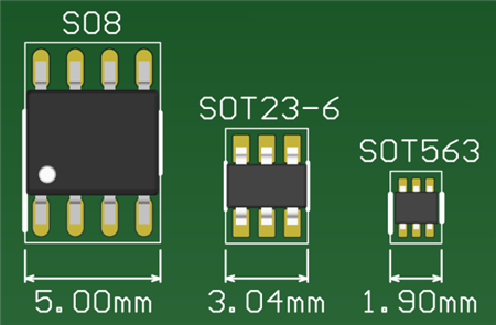
One obvious way to reduce your solution size is to choose an integrated circuit (IC) in a smaller package. Small-outline (SO)-8 and small-outline transistor (SOT)-23-6 packages are common for 12-V voltage rail DC/DC converters. They are typically very reliable. However, if you work in an industry where every millimeter counts – such as the drone market – you may be looking for an even smaller DC/DC converter. The SOT-563 package is almost 260% smaller than the SOT-23-6, and 700% smaller than the SO-8 package. Figure 1 compares the size of the mechanical outline of all three packages.

Figure 1: Mechanical outline sizes of three converter packages

Apart from choosing a smaller package, another approach to reducing your solution size is to reduce the output inductor and capacitor. Equations 1 and 2 calculate the output inductance (LOUT) and output capacitance (COUT)


where ris defined as the ratio of current ripple of inductor, VRIPPLE is the maximum allowed peak-to-peak ripple voltage and fsw is the switching frequency of the converter. Because LOUT and COUT are both inversely proportional to fsw, the larger the switching frequency, the smaller the LOUT and COUT.  Smaller inductance or capacitance means engineers can select an inductor or a capacitor of a smaller size. Converters with a higher fsw can work with these smaller inductors and capacitors.

Addressing thermal performance

A smaller system faces more significant thermal performance issues, given the limited path for heat dissipation. To effectively solve any possible thermal issues and achieve higher efficiency, you can apply converter switches with a lower RDS(on). Equation 3 calculates the temperature rise on a DC/DC converter:

where PLOSS is the total power loss of the converter and RΘJA is the junction-to-ambient thermal resistance.Consider a 2-A load converter with an average RDS(on) change from 100 mΩ to 50 mΩ. The power loss of this device will result in a 200-mW decrease, which will bring a 16°C cooldown on a typical SOT-563 board with a thermal resistance of 80°C/W. Therefore converters with a lower RDS(on) offer better working conditions at a lower temperature.

Turning theory to practice

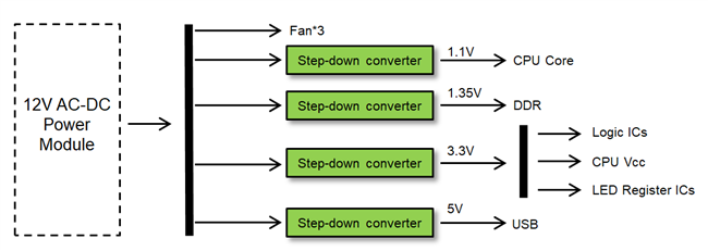
A real-world embedded system often applies multiple step-down DC/DC rails. Figure 2 shows a block diagram of a home router power-stage architecture that needs four lower voltage rails. Let’s take three typical devices applied in this type of system to demonstrate how package size and switching frequency affect power rail solution size.

Figure 2: Power-stage architecture of an embedded system
 
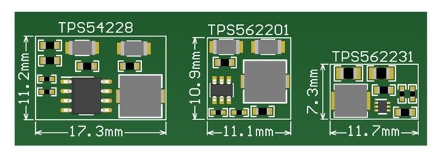
The TPS54228 has a 700-kHz frequency in an SO-8 package. The TPS562201 has a 580-kHz frequency in an SOT-23-6 package, and the TPS562231 has a 850-kHz frequency in an SOT-563 package. The TPS562231 has the highest frequency and the smallest IC package size. This solution size is about 142% smaller than the TPS562201, and 227% smaller than the TPS54228, as illustrated in Figure 3.

 
Figure 3: Solution sizes of converters with different packages
 
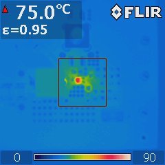
The RDS(on) of the integrated metal-oxide semiconductor field-effect transistor (MOSFET) in the TPS562231 is 95 mΩ (high side) and 55 mΩ (low side). Figure 4 is a thermal image of the full load temperature rise of a 12-V input on the TPS562231 evaluation board.

 
Figure 4: Thermal image of the TPS562231 with a 12-V input voltage
  
In general, the TPS562231 works in an 850-kHz switching frequency sealed in a small SOT-563 package, which can help reduce the overall solution size. Its low on-resistance also allows for good thermal performance. It’s suitable for routers, drones, set-top boxes or any other embedded designs that require small solution sizes.
 
Additional resources


How SysConfig jump-starts embedded system development

$
0
0

One of the significant challenges for embedded systems developers is how to efficiently and accurately configure their systems. Today’s advanced microcontrollers (MCUs) include a variety of processor cores, hardware accelerators, advanced radios, sophisticated peripherals and interfaces, and come in packages with elaborate pin multiplexing schemes.

Software examples from many semiconductor suppliers can provide a starting point for embedded designs, but developers typically have to make modifications to various parameters, events and variables in order to optimize the software for a specific application. These modifications often entail reviewing many pages of technical documentation to identify and update specific registers or lines of source code. Such manual modifications can be error-prone given the complexity of the code sequences and variety of naming conventions. The number of updates may grow exponentially as well, depending on the number of options a given software component supports and the number of options used by the desired application. Manual updates can also introduce resource conflicts that aren’t detected until much later in the build process, leading to frustration and potentially multiple wasted iterations.

To help simplify configuration challenges and accelerate software development, TI created SysConfig, a unified software configuration tool with an intuitive and comprehensive collection of graphical utilities for configuring pins, peripherals, radios, subsystems, and other components. SysConfig helps you manage, expose and resolve conflicts visually so that you have more time to create differentiated applications.

SysConfig displays all configurable parameters in a graphical user interface with configuration options in drop-down lists. As you interact with SysConfig, mouse overs, tool tips and visual cues guide you toward a valid configuration. Contextual documentation is embedded directly within the interface, and relevant documentation and definitions are exposed and linked within the tool, giving you the right information to help you configure your software when you need it. You no longer have to search through numerous documents and lines of source code trying to figure out how to update a parameter; instead, you can quickly create your initial configuration and spend more time innovating within your application, with TI LaunchPad™ development kits or your own custom hardware.

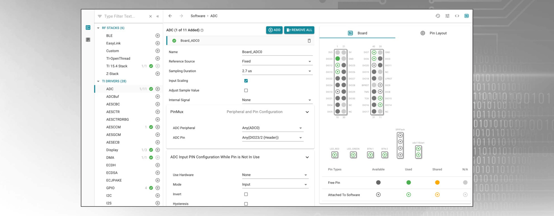
SysConfig is intelligent. Board views for LaunchPad development kits show the pins used on the board as well as the expansion headers shown in Figure 1. SysConfig understands what pins and resources the application is already using and can help auto-solve potential conflicts as you enable and configure additional components. For example, if you were to add in an analog-to-digital converter (ADC) instance to the project, SysConfig will find and assign the next available ADC peripheral and pin automatically. It is easy to add resources using the plus sign, with drop-down menus helping organize the available options. Color coding helps indicate conflicts, shared resources, and successful allocations.

Figure 1: An example LaunchPad development kit board view

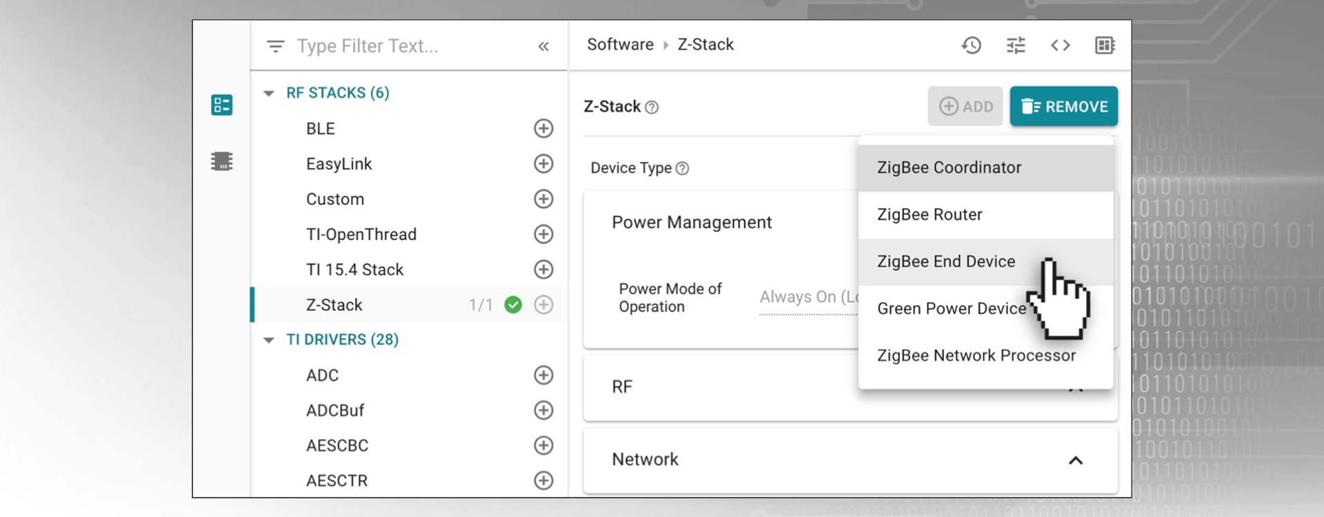
SysConfig’s device view is useful for custom hardware development with a similar level of information. Software views, such as the one shown in Figure 2 for Z-Stack configuration, provide a comprehensive view of configurable parameters. A list of options is displayed for each parameter (Zigbee device type in this example). The default setting is being changed from Zigbee Connector to Zigbee End Device with a simple mouse click. Hover over the “?” icon with a mouse and additional details on these parameters will be displayed while the newly updated software will be shown in the preview pane. With this initial release, SysConfig supports the configuration of pins and drivers for most SimpleLink™ MCUs, including the configuration of radio-frequency (RF) parameters and stacks for wired and wireless communication technologies like Wi-Fi®, Ethernet, Bluetooth®, Zigbee®, Thread, 15.4 and EasyLink. It also supports multiprotocol configuration. You can easily update the default settings to quickly find the optimal combination of RF and stack settings for your use case. You can also export the parameters to other TI tools, including TI’s Smart RF™ Studio, for further testing and tuning. 

Figure 2: An example stack configuration view

SysConfig is now available in TI’s Code Composer Studio™ integrated development environment (IDE) for both desktop and cloud. It is also available as a stand-alone tool for use with other IDEs, including IAR Embedded Workbench for Arm® processors.

SysConfig’s capabilities will continue to expand over time. The tool will follow the quarterly release cadence of the SimpleLink software development kit, introducing new features and capabilities to continue improving developer efficiency.

Additional resources

Watch our Connect video series on SysConfig:

Access the SysConfig tool folder

Address thermal performance in small applications with the power WCSP technology

$
0
0

When it comes to cost-effectively powering space-constrained, high-power-density applications, such as solid-state drive (SSD) or wearable equipment, wafer chip-scale package (WCSP) DC/DC converter solutions are widely used in the industry. The trend toward even tighter integration into system-in-package (SIP) modules poses an increasing challenge to established packaging techniques, forcing engineers to look for new ways of optimizing thermal performance in space-constrained applications.

Thermal performance and solution size, particularly maximum profile height, are very real challenges that every SIP designer experiences. As the designer of a low-form-factor SIP module for your next application, you may be searching for a power device that will fit in the tiny space you have and that will also stay cool while delivering the power you need for your system.

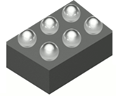
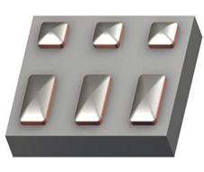
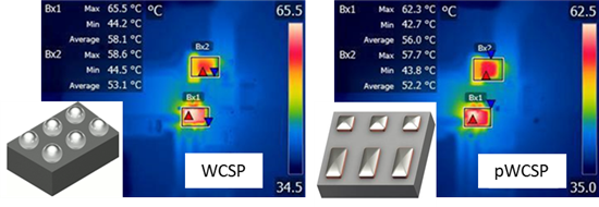
TI’s power chip-scale packaging (power WCSP) is a low-profile WCSP enhancement that focuses on thermal performance and current density optimization. Unlike a standard WCSP, which uses a fixed ball diameter (Figure 1a), power WCSP takes advantage of the flexibility of copper post sizes to increase the area of key interconnects like power pins, without having to increase the die size or infringe upon the spacing tolerance of surface-mount manufacturing technologies. The copper posts can be square or rectangular, with a total stack thickness as small as 85 µm (Figure 1b). The shape of the posts makes it possible to achieve a significant surface gain for critical pins, thereby increasing current-handling capacity as well as improving the heat transfer and thermal performance of the package. At the same time, the package height can be as low as 0.3 mm, enabling easy implementation into high-power-density and space-critical integrated solutions.

Figure 1: 6-pin standard WCSP package (a); 6-pin power WCSP package (b)

TI’s TPS62088 DC/DC converter demonstrates the thermal performance of power WCSP packaging. The TPS62088 is a 1.2-mm-by-0.8-mm, high-efficiency 2.4-V to 5.5-V input, 3-A DC/DC buck converter operating at a 4-MHz switching frequency. The device is available in two package options: either the standard WCSP (TPS62088YFP) or the new power WCSP (TPS62088YWC). Looking at the thermal properties of these otherwise identical devices in each package option allows us to make a clear comparison of the thermal performance of the two packaging technologies.

Figure 2a shows the thermal performance of the TPS62088YFP (WCSP) and Figure 2b shows the TPS62088YWC (power WCSP) operating at VIN = 5 V, VOUT = 1.8 V and IOUT = 3 A, taken at room temperature with an infrared camera. Due to very low junction-to-top characterization parameter values – ΨJT = 0.5-0.7°C/W for both packages – you can assume that the junction temperature is roughly equal to the case temperature. The results indicate that the temperature of the power WCSP device is reduced by as much as 3°C compared to the standard WCSP device, considering the device and printed circuit board (PCB) layout solution together.

The TPS62088YWC power WCSP version, while increasing power density by reducing profile height from 0.5 mm to 0.3 mm, enables you to optimize the thermal performance of your system by improving the heat transfer to the PCB through the larger bump structures. Of course, designing your application for optimal thermal performance implies paying attention to further aspects of the system as well. Proper PCB layout results in smaller junction-to-ambient and junction-to-board thermal resistance, thereby reducing the device junction temperature for a given dissipated power and board temperature. Wide power traces can also efficiently sink dissipated heat. Keep in mind that many system-dependent properties such as thermal coupling, airflow, added heat sinks and convection surfaces, and the presence of other heat-generating components, affect the power dissipation capabilities of a given device.


Figure 2: Thermal performance of the TPS62088 (measurement point: Bx1) operating at VIN = 5 V, VOUT = 1.8 V and IOUT = 3 A taken at room temperature: TPS62088YFP WCSP version (a); TPS62088YWC power WCSP version (b)

Many space-constrained applications like SIP modules, SSDs or wearable devices, require the total power solution, (not just the power IC), to fit in the thinnest spaces possible. The TPS62088YWC’s high switching frequency allows you to use tiny, low-form-factor 0.24-µH inductors to shrink the solution size to 15 mm2, and take full advantage of the 0.3-mm profile height for the whole power circuit.

Additional resources

How to choose the right proximity sensor for your design needs

$
0
0

This post was co-written with Rahland Gordon and Robert Ferguson.

As the world becomes increasingly automated, it’s imperative for the technology we interact with every day to detect and respond to ever-changing environmental factors. For example, vacuum robots must course-correct based on furniture placement, and automatic doors should open and close based on movement detection. These reactions need to occur for a range of distances and materials, regardless of their behavior, color or size.

The good news is that no matter what environment you need to monitor, there are a range of proximity sensors from which to choose, including ultrasonic, optical time-of-flight (ToF) and millimeter-wave (mmWave) sensors. Selecting the right option may not always be intuitive, so this article will offer guidelines for choosing the best proximity sensor to meet your design needs.

For quick comparison guide, see our proximity sensing technology infographic.

Ultrasonic sensors

Ultrasonic sensors are particularly powerful in sunny, transparent, liquid, and light or dark environments. Because ultrasonic sensing works regardless of ambient lighting conditions (as it uses sound waves rather than light waves), ultrasonic sensors are particularly advantageous in outdoor environments where other sensing technologies may fail due to bright, ambient lighting conditions.

TI’s PGA460, pictured in Figure 1, offers effective, low-cost proximity and obstruction detection for solid and transparent glass surfaces, in addition to smoky and gas-filled environments.

Figure 1: PGA460 functional diagram

Optical ToF sensors

Optical ToF sensors offer different advantages, such as excellent performance under high temperatures, humidity and air pressure. Unlike other forms of proximity sensing (such as capacitive or inductive sensing), optical ToF sensors can reach long distances, upwards of 20 m. In addition to its long-range capabilities, its field of view can be narrowed to focus on an exact target. This makes optical ToF sensors a good fit for applications like displacement transmitters and drone landing systems.

TI’s OPT3101, pictured in Figure 2, has the unique ability to support up to three separate emitters, allowing for multizone use. Multiple zone detections specify which zone the target is in, thus providing data on both the direction and distance of the target. With this information, design engineers can determine the behavior of the target, like whether a person is approaching a kiosk or simply walking by.


Figure 2: OPT3101 functional diagram

mmWave sensors

mmWave sensors enable systems with millimeter-level accuracy, detecting objects or people without infringing on personal privacy in any environmental conditions. What may be even more impressive about mmWave sensors is that they provide a very unique set of data for each object or person detected, including its range, velocity and angle. No other single sensor can provide such information. mmWave sensors deliver high accuracy in three key areas:

  • The ability to see in all conditions and know a person’s exact location in order to better integrate with optical solutions for facial recognition.
  • Collaborative robots working in near proximity to humans don’t have to stop when humans approach, but rather can continue working at a potentially slower rate.
  • Automatic doors and gates save power and energy by only opening only when someone approaches at the correct angle, not just passing by with no intention to enter.

TI mmWave sensors take all of these benefits a step further by integrating processing engines to enable application algorithms to run on the mmWave device itself, removing the need for additional processors in the system to save on cost, power and size.

From self-driving cars and smart buildings to the smallest of watches, systems are making decisions based on what they sense in real time. Our infographic and additional resources are meant to help in this data-rich selection process.

Additional resources

How to save space and BOM costs by sharing microphones across automotive subsystems

$
0
0

In the cost-driven automotive industry, reducing bill-of-materials (BOM) costs by sharing resources across multiple subsystems (when possible) can give manufacturers an edge. Traditional automotive end-equipments often use independent hardware to control specific functions of the car, and chances to combine functions may be overlooked.

Sharing microphones between different automotive audio subsystems not only saves automakers the cost of a microphone – it eliminates the cost associated with microphone plastic enclosures, wiring and installation. These costs likely outweigh the cost of a microphone or a codec. In this article, I’ll discuss an effective way to share hands-free voice command recognition and eCall microphones using TI’s automotive-grade TLV320AIC3109-Q1, TLV320AIC3104-Q1 and TLV320AIC3106-Q1 audio codecs.

A typical application of microphones in vehicles

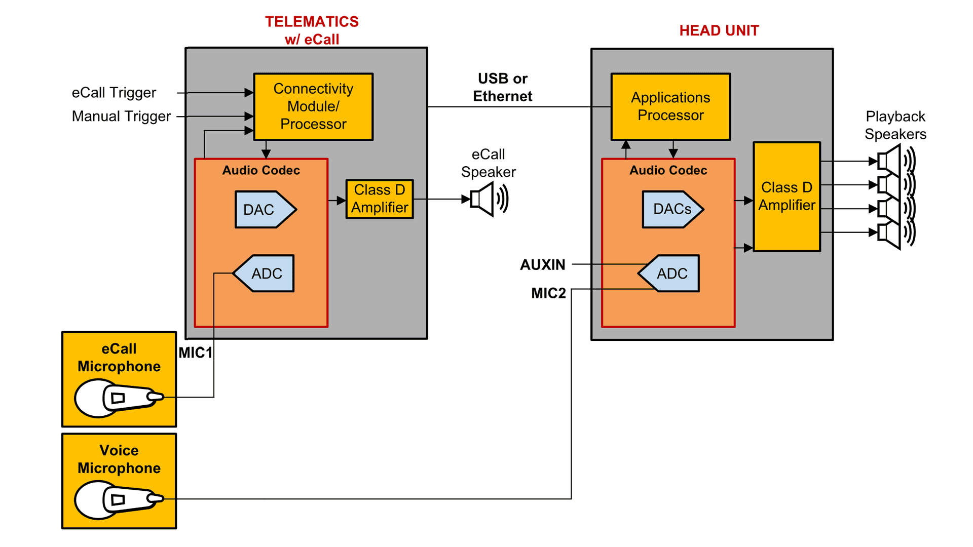
As shown in Figure 1, a typical telematicssystem with eCall has one dedicated microphone for direct audio communication between the car and local emergency services in an emergency. The microphone signal is digitized using an analog-to-digital converter (ADC) inside a codec, and is eventually transmitted to emergency operators through a connectivity module.

A typical head unit has two audio input sources: one line input to support playback from portable audio output devices such as smartphones and MP3 players, and a microphone input for voice command recognition and hands-free telecommunication.

Therefore, most vehicles use at least two dedicated microphones: one for eCall applications and another for voice command recognition and hands-free telecommunication applications.


Figure 1: A typical application using dedicated eCall and voice microphones


Sharing a microphone for eCall and voice command recognition

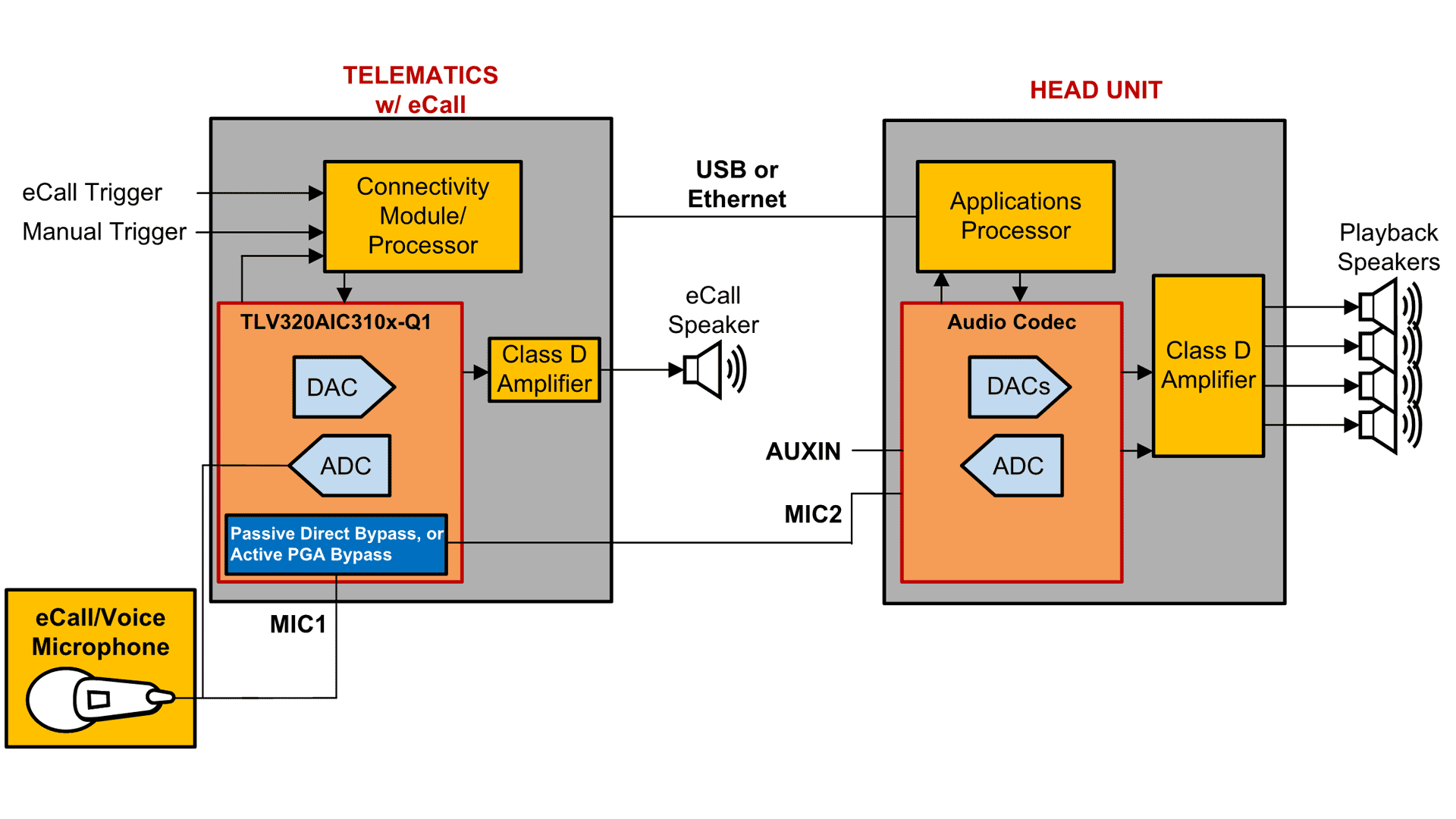
TI’s automotive-grade TLV320AIC3109-Q1, TLV320AIC3104-Q1 and TLV320AIC3106-Q1 audio codecs offer two special modesthat allowthe microphone signal to be routed to the ADC of the codec for eCall and also to the head unit for voice command recognition:

  • Passive direct bypass mode establishes a direct connection from microphone input to line output, in addition to the regular ADC path. This mode allows the microphone signal to be bypassed directly to the line output passively, without any amplification.
  • Active PGA bypass mode establishes a buffered connection from microphone input to analog output through a PGA and a mixer, in addition to the regular ADC path. This mode allows the amplification of the microphone signal (if necessary) before the signal is routed to the line or headphone output.

As shown in Figure 2, these modes enable you to eliminate one microphone from the system altogether, resulting in reduced cost and space associated with the second microphone, along with reduced cable routing and microphone installation costs.


Figure 2: Sharing eCall and voice microphones using TLV320AIC310x-Q1 devices 

The application note, “Different Configurations in TLV320AIC310x-Q1 Codec Family to Enable Sharing eCall and Hands-Free Voice Microphones in Vehicles,” explains the different possible configurations, along with example pseudo-code, in both passive direct bypass and active PGA bypass modes.

Additional resources

Solving lifetime and temperature challenges in AC motor drives with capacitive-based isolation

$
0
0
Every day, we see systems in motion all around us, driven by motors. AC motor drives are the most common type of motor drive. They’re used in a variety of industrial applications, such as air conditioning in commercial buildings and factory automation...(read more)

Current-sensing dynamics in automotive solenoids

$
0
0

During my first visit to the U.S., my brother and I drove from New York City to Columbus, Ohio. Although the 650-KM (400-mile) journey was long, our car’s automatic transmission and cruise control made the trip more comfortable. The effectiveness of an automatic transmission and cruise control relies on the precise control of proportional solenoids and motors, which is made possible with accurate current measurement.

Proportional solenoids convert electrical signals into a proportional mechanical force, which allows variance in armature position and force relative to the level of current. Proportional solenoids are used in automotive applications such as automatic transmissions, fuel injection systems, pistons and valves to accurately control position or flow. Controlling proportional solenoids precisely is highly dependent on the accuracy of the position estimation over the automotive temperature range. In general, measurement is used to provide position for proportional solenoids. 

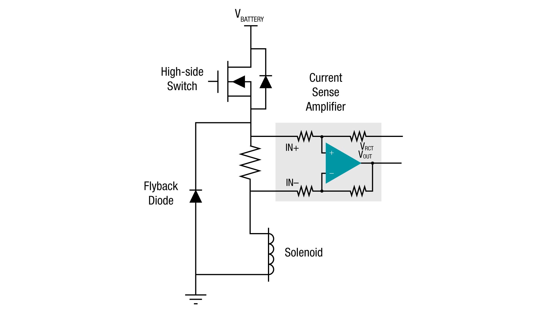
As shown in Figure 1, a shunt resistor is inserted in between the switch and the solenoid. The low-ohmic shunt is inserted in such a way to create a low resistance path as well as safely measure and accommodate recirculation current flows. An amplifier in a differential configuration or current sense amplifier is connected to the shunt to measure the current.

Figure 1: Solenoid current measurement

A pulse width modulation (PWM) signal operates the high-side switch. When the PWM is high, the battery connects to the solenoid and current flows. When the PWM is low, the battery disconnects from the solenoid and recirculation current flows through the flyback diode.

The control of the PWM frequency and duty-cycle percentage determines the resulting average current in the solenoid, which in turn controls the force applied to the actuator.

Sensing accuracy
Nominal current ranges for solenoids vary from device to device. Because of differing current range needs, current sense amplifier selection for these types of systems is critical as the necessary precise movement of the entire solenoid system depends on the accuracy of the current measurement.

Solenoid current sensors can be designed with external shunts or integrated shunt devices depending on the accuracy requirement. Each has their own advantages. Tables 1 and 2 summarize the differences and benefits of these two architectures.


External shunt devices

Integrated shunt devices

Suitability

Lower-current solenoids, because it is possible to interface with a higher-value external shunt resistor

Higher-current solenoids, as the integrated shunt is 2 mΩ. Choose based on your accuracy requirement.

Differential configuration register placement

Integrated

Integrated

Temperature drift

Shunt tolerances independent of device tolerance specifications, with considerable drift over the temperature range

Shunt tolerances included in device tolerance specifications, implying less drift over the temperature range

Resistor quality

  • External resistor enables system-level flexibility on maximum current rating
  • Attention to PCB traces to shunt for measurement accuracy
  • Total system error dominated by shunt quality
  • Fixed ±15-A maximum current rating
  • Ease of design
  • Factory-trimmed to guarantee overall system reduction
  • Integrated 3-nH low inductive shunt with low drift over temperature (15 ppm/°C)
  • 0.1% integrated 2-mΩ shunt resistor
  • Fixed ±15-A maximum current rating
  • Ease of design
  • Factory-trimmed to guarantee overall system reduction
  • Integrated 3-nH low inductive shunt with low drift over temperature (15 ppm/°C)
  • 0.1% integrated 2-mΩ shunt resistor 

Kelvin connection

External

Internal

Common-mode voltage

-4 V to 80 V

-4 V to 80 V

Table 1: Differences for external and internal shunt devices. 


External shunt devices

Integrated shunt devices

Benefits

  • High common-mode rejection ratio enables direct in-line motor current sensing
  • Simplifies system design, enabling faster time to market
  • Flexibility for various current ranges and also easily manageable
  • High common-mode rejection ratio enables direct in-line motor current sensing
  • Simplifies system design, enabling faster time to market
  • High accuracy minimizes system margins and potentially eliminates system-level calibration
  • Low inductance reduces PWM spikes and improves measurement accuracy
    _________________________________

  • Novel approach to handling high common-mode voltage transients
  • Instead of using a high bandwidth amplifier, can implement a circuit to filter these input transitions from reaching the output buffer
  • Novel approach to handling high common-mode voltage transients
  • Instead of using a high bandwidth amplifier, can implement a circuit to filter these input transitions from reaching the output buffer

  • High common-mode rejection ratio enables direct in-line motor current sensing
  • Simplifies system design, enabling faster time to market
  • High accuracy minimizes system margins and potentially eliminates system-level calibration
  • Low inductance reduces PWM spikes and improves measurement accuracy
    _________________________________
  • Novel approach to handling high common-mode voltage transients
  • Instead of using a high bandwidth amplifier, can implement a circuit to filter these input transitions from reaching the output buffer

Enhanced PWM rejection system-level benefit

  • Substantially reduced “blanking time”
  • Accurate measurement at lower duty cycles
  • Substantially reduced “blanking time”
  • Accurate measurement at lower duty cycles
  • Substantially reduced “blanking time”
  • Accurate measurement at lower duty cycles

Inclusion of flyback period in measurements.

Required wide common-mode range to accommodate the solenoid flyback period

Required wide common-mode range to accommodate the solenoid flyback period

Inductance

Low, in order to reduce voltage swings during state transitions

Low, in order to reduce voltage swings during state transitions

Price

Relatively lower price (excluding shunt price)

Moderately higher (including shunt price)

Relevant TI reference design

Reference Design for Automotive, Proportional-Solenoid Current Sensor

Automotive Proportional Solenoid Drive with Highly Accurate Current Sensor Reference Design

Table 2: Benefits of external and integrated shunt devices.

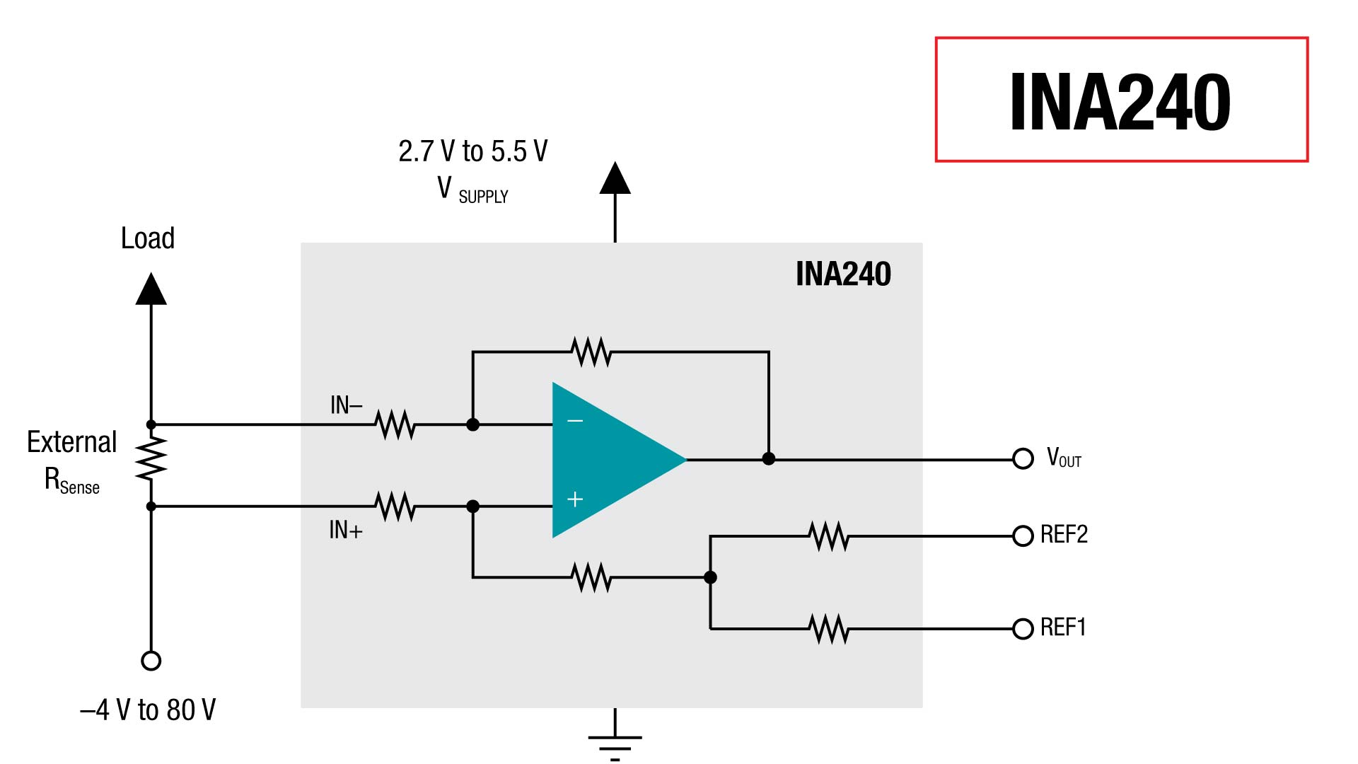
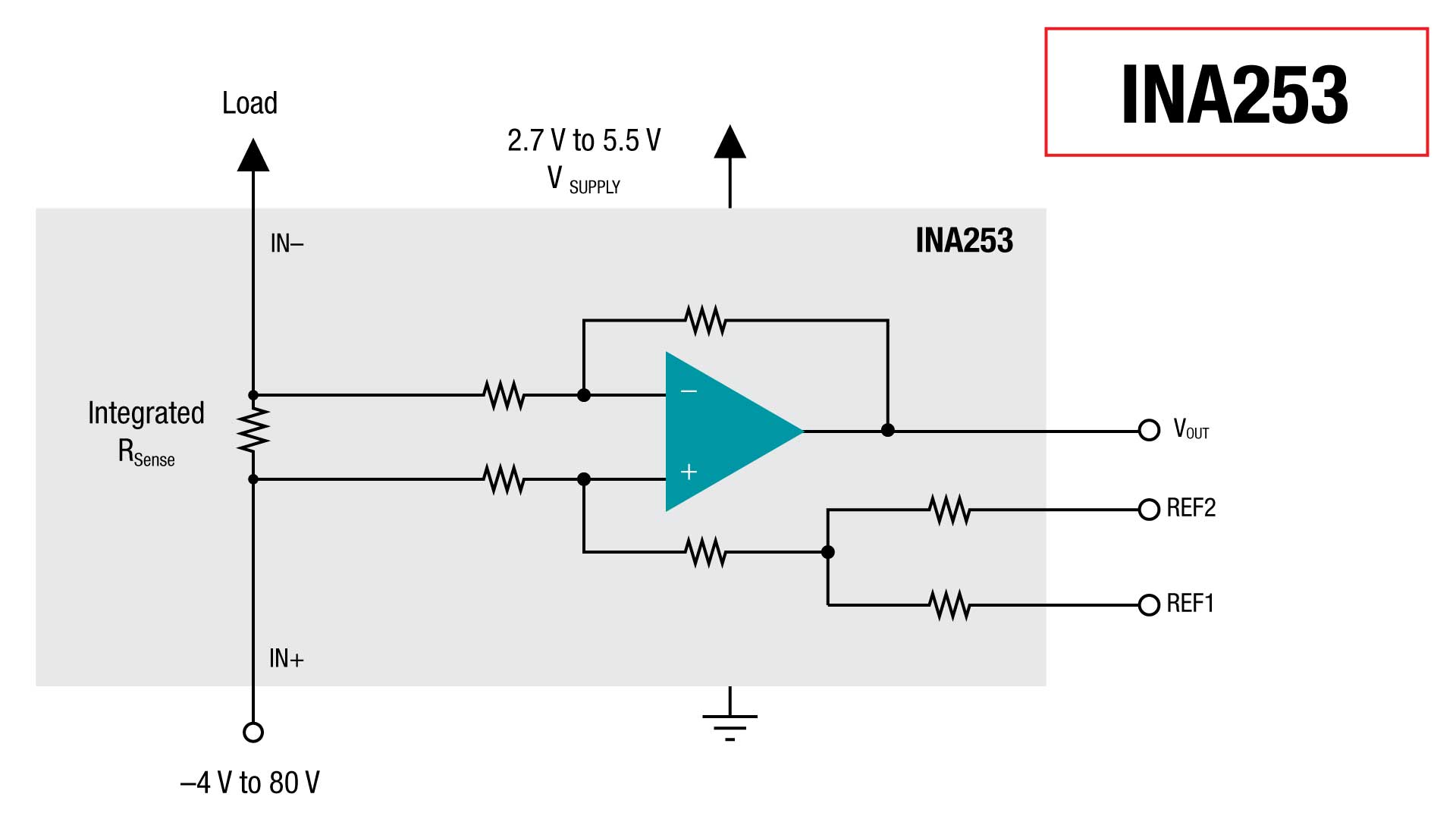
Figure 2 and 3 shows the configurations of shunt for external and internal configurations. In Figure 2 shunt is external to the device (INA240-Q1) and in Figure 3 shunt is internal to the device (INA253-Q1).

Figure 2: External shunt configuration with INA240

Figure 3: Internal shunt configuration with INA253

Maintaining solenoid current sensing accuracy

The impedance of a solenoid comprises inductive and series resistive components. The series resistance of the coil (typically copper) has a high-temperature drift of 4,000 ppm/°C. This high drift value may correspond to a 40% accuracy reduction in solenoid motion control over a 100°C range.

Accuracy at lower current ranges is essential over the entire temperature range mainly because lower currents are noise prone and there is a more chance for the solenoid position inaccuracies. Smooth operation of hydraulic systems requires a minimum 2-mA resolution. Variations in this resolution cause solenoid position inaccuracies.

TI has two devices designed for solenoid current sensing applications:

  • The INA240-Q1 enhances PWM rejection and has significantly lower offset and gain drifts over the temperature range, minimizing error at a 2-mA resolution.
  • The INA253-Q1 is a low inductive 3-nH 2-mΩ integrated shunt with a drift at 15 ppm/°C. Placing the INA253-Q1 in series with the solenoid, the drift accuracy can decrease overall end-equipment system errors from 40% to 0.15%.

These devices have increased the effectiveness of our powertrain, motor-control circuits and automotive battery systems.

Conclusion
Automotive solenoids need higher accuracies to compensate for wider temperature ranges and increased drift as the temperature increases. Our current-shunt monitors enable accurate readings across the entirety of automotive temperature ranges.

Additional resources


Basic considerations for sensors in the powertrain

$
0
0

powertrain

Designing a better powertrain is the most significant way to reduce automotive emissions. Whether it’s improving the efficiency of a combustion engine or designing electric vehicles (EVs) or hybrid electric vehicles (HEVs), electrification is powering a massive evolution of the powertrain as we know it.

powertrain

This white paper, Basic considerations for sensors in the powertrain, examines the future of powertrain sensors through the electrification of a vehicle in internal combustion engines (ICEs) and sensors in EVs and HEVs, and their importance in optimizing the powertrain for effectively managing the battery, inverter and motor building blocks.

Addressing high-voltage current-sensing design challenges in HEV/EVs

$
0
0

Electrification has created a new paradigm in automotive power systems; whether the design is a hybrid electric vehicle (HEV) or fully electric vehicle (EV), there are new design challenges to address. In this technical article, I’d like to highlight some of the primary challenges in high-voltage current sensing and share additional resources to aid and simplify your design process. 

For an introduction to current sensing, see our e-book, “Simplifying current sensing.” 

High voltage, high current (>200 A or, more commonly, 1,000 A)

High voltage (≥400 V) fully electric systems aim to lower the current consumption for the traction system that moves the vehicle. This requires isolating the solution so that the “hot,” high-voltage side can provide current measurement to the “cold” side (attached to low-voltage ≤5-V microcontrollers or other circuitry). The high current presents an issue when trying to measure with a shunt resistor due to the I2R power dissipation. 

To use a shunt in these conditions means that you must select a sub-100-µΩ shunt resistor, but these resistors tend to be larger and costlier than more common milliohm resistors. One alternative is to use magnetic-based solutions, but these are less accurate and have higher temperature drift than shunt-based solutions. Overcoming these performance drawbacks will dramatically increase the cost and complexity of a magnetic solution as well. 

Learn more with these design resources: 

High voltage, low currents(>400 V and <500 A)

Again, high voltages require an isolated solution. From a current perspective, anything below 100 A tends to be a shunt-based solution. Between 100 A and 500 A, choosing between a shunt or magnetic solution requires trade-offs between cost, performance and solution size. This white paper explains: 

Precision measurements on the 48-V rail, low current (<100 A)

The main design challenge with a 48-V rail is the survivability voltage necessary to meet your requirements, which may be as high as 120 V. In some 48-V motor systems, precision current measurement is required to enable peak motor efficiency. These motor systems may include a traction inverter, electronic power steering or a belt-start generator. In-line measurement provides the most precise representation of actual motor current but is also very challenging due to the presence of high-speed pulse-width modulation (PWM) signals, as explained in: 

For non-motor 48-V systems, such as DC/DC converters or battery management systems (BMSs), implementing bidirectional DC current measurement is more critical than switching performance, as explained in:

Remove high voltage common-mode voltage requirements with low-side sensing
Low-side current sensing reduces some of the amplifier requirements: the inputs do not need to survive a high voltage, as the common mode for low-side sensing is ground – 0 V. 

The amplifier’s common-mode voltage range must include 0 V in order to measure on the low side. If the application is motor low-side phase-current measurement, the amplifier must have a high slew rate to adjust for the switches turning on and off, as explained in: 

For non-motor applications, the choice of what you use is based on the implementation’s accuracy requirements. See: 

Measuring multidecade current in BMSs

High-precision, multidecade current measurement (from milliamperes to 1 kA) is a significant challenge to address in a single solution. Magnetic solutions do not measure low currents well due to their high offset levels and significant drift. Shunt-based measurements require very low offset to be able to measure low currents on a sub-100-µΩ shunt resistor due to the very low differential input voltage level. 

For example, a BMS may want to measure ±1,500 A. In a bidirectional measurement with a ±2.5-V output swing relative to the 0-A output voltage and a gain of 20, the maximum input voltage is ±125 mV. This results in a shunt resistor value of ≤ 83 µΩ. The voltage drop across this shunt at 100 mA is only 8.3 µV, which means that you’ll need an amplifier system with very low offset to be able to measure this level. If the system has 1 µV of offset, your error at this level is ~16%. 

To learn more, read: 

Current sensing in solenoids for a smoother drive

Many automotive applications use proportional solenoids, but when it comes to high-voltage current sensing, proportional solenoids are mainly used in automatic transmissions. Proportional solenoids provide a smooth driving experience when shifting the clutch and gears or operating hydraulic fluid pumps. The drivability of a solenoid mainly depends on two factors: solenoid drive and solenoid position sense. 

High-accuracy current measurement enables precise closed loop-control of the solenoid plunger position. 

Current sensors in solenoid applications follow a shunt-based principle. Pulse width-modulation signals are made to flow on the solenoid through milliohm shunts. Depending on the current range, this milliohm shunt is integrated or external to the current-sense amplifier. 

For more details about solenoid current sensors, check out: 

Current sensing is a foundational element for the increased electrification in automotive design, particularly in high-voltage systems. Modern cars are requiring more from sensors than ever before, but the resources I’ve linked to in this article can help you design a powertrain that’s equipped for strong performance and safe power delivery.

Thanks to my colleague Sandeep Tallada for contributing his expertise to the solenoid portion of this article.

Powering tiny industrial automation control equipment with high-voltage modules: how to ensure reliability

$
0
0

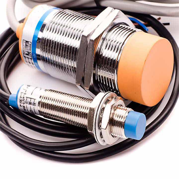
It’s not unusual to find industrial automation control equipment like field sensors (for proximity, pressure, flow or temperature, for example) housed in increasingly inconspicuous packages. Figure 1 shows an example of a proximity sensor housed in a tiny screw (which can be as small as 8 mm or in some instances even smaller). While the electronics that go into the housing have to be ultra-small, they still need to be rated for the right parameters to ensure long-term equipment reliability.

Figure 1: Typical proximity sensor

Addressing the challenges of unregulated input voltages

Electronics in smart sensors may include a low-power microprocessor, analog-to-digital signal-processing circuitry and a voltage regulator. Sometimes, designers might not consider power until the end of the design process; therefore, the space allotted to power can be really sparse.

A typical application for power-conversion circuitry in factory automation equipment might be down-converting a 24-V input voltage and regulating it to the required potential. The 24-V input voltage might be a standard industrial bus which could have an input voltage as low as 8 V or as high as 36 V.

Sensors in process automation need to withstand overvoltage transients. The severity of voltage transients depends on how the 24 V was derived. In some situations, where the lead lengths cover long distances in the field, the industrial 24-V bus may experience higher voltage transients. In addition, field applications could have clamp circuits that limit the voltage transient to a safe extra-low voltage limit. This means that in a short-circuit condition; the output of the industrial bus could be stuck at 60 VDC.

Considering another example, a 24 VAC could be an input source. The maximum root-mean-square voltage of such a supply can often swing to 28 V, leading to a peak voltage delivered that’s close to 40 V. The overvoltage protection setting on the input supply could be about 120% of the peak voltage, which takes an input voltage close to 48 V.

In these examples, it is important to use a voltage regulator rated for the maximum DC voltage at the input to ensure uninterrupted operation of equipment like field sensors.

Ensuring appropriate pin spacing for long-term reliability

The TPSM265R1 is a high-voltage embedded power module rated for 65 V that integrates the voltage regulator and inductor. This gives the device enough margins to cover potential overvoltage conditions. However, just because a power module has an integrated high-voltage regulator doesn’t mean that you can safely rate it for the high voltage. To properly rate the device for a higher input voltage requires appropriate design of the pad/pin spacing on the module. The Association Connecting Electronics Industries has a standard called IPC 2221-B which goes over this in detail.

The IPC-2221B standard lists the minimum spacing between the edges of conductors that is required to ensure proper operation at worst-case voltages. To ensure that the regulator can indeed sustain a peak voltage of 65 V the spacing between the edges of the conductors must be at least 0.5 mm.

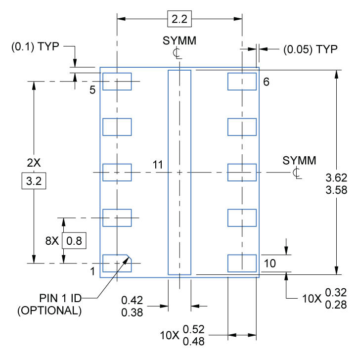
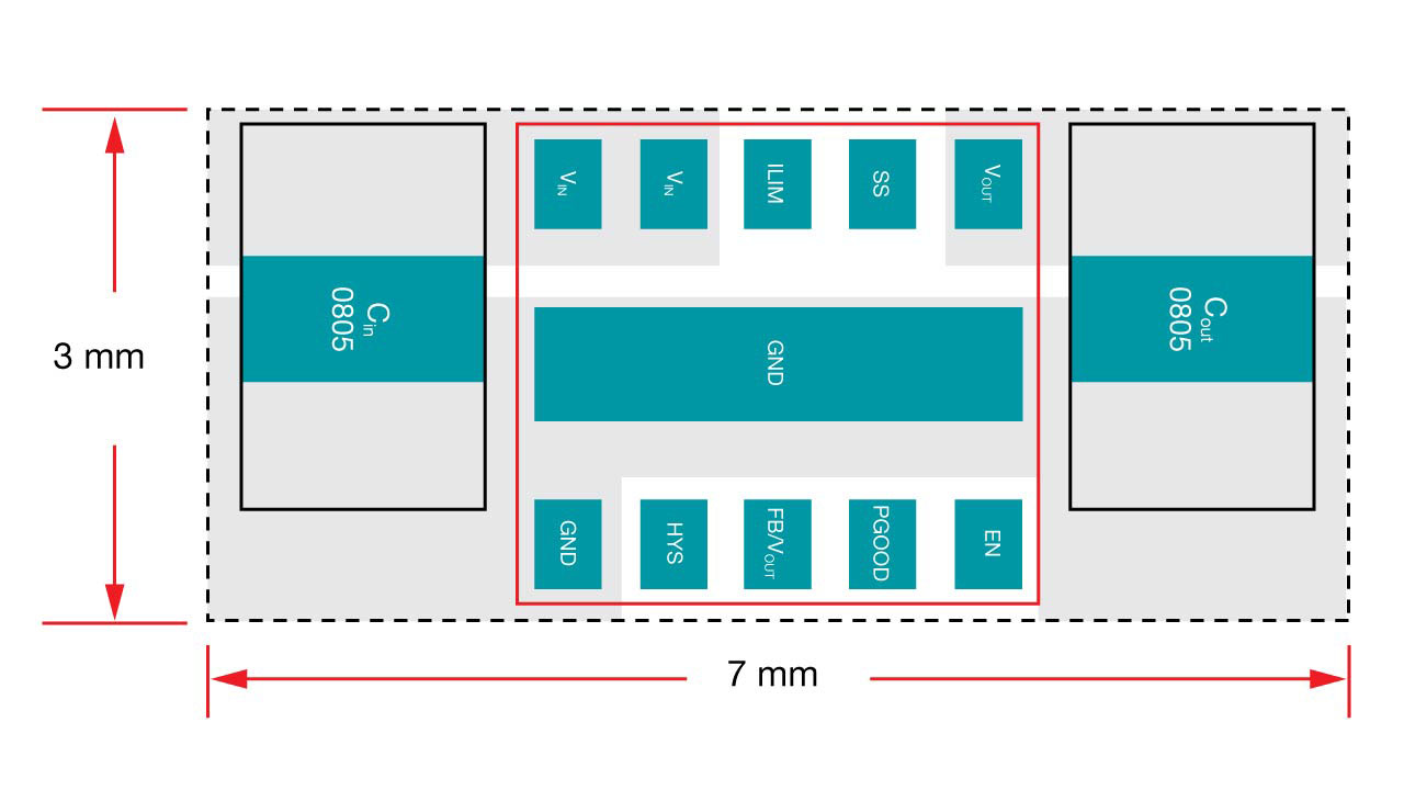
Figure 2 shows the pin pitch of the TPSM265R1, which is 0.8 mm; the width of the pad is typically 0.3 mm. From edge to edge, the space between the pads is 0.5 mm, in compliance with the IPC-2221B requirement.

Figure 2: TPSM265R1 package drawing

Meeting the requirement for a small solution size

IPC spacing requirements put system designers at odds with the requirement for miniaturization. After all, I began this technical article talking about how electronics need to fit into an 8-mm screw. To address both spacing requirements and miniaturization requirements, designers have to be smart about designing the power module. TI designed the layout of the TPSM265R1 package with a small-solution space in mind. Figure 3 shows an example layout, with the minimum required components for a fixed-voltage option of 3.3 V or 5 V.

Figure 3: Example layout with the TPSM265R1

The module package size is 2.8 mm by 3.7 mm. To complete the circuit, you only need two capacitors. With two 0805 capacitors, the overall solution size for a 5 V or 3.3 V output can be as small as 3 mm by 7 mm. The placement of the input capacitor so close to the module’s VIN and GND pins makes for a “quiet” switching operation, with less ringing on the switch node.

When designing the power supply for small industrial automation control equipment, it’s important to choose products with appropriate ratings for a reliable operation. Well-designed power modules will not only help engineers address size challenges and ensure long-term reliability but can also help simplify the design process.

Additional resources

Innovate, accelerate and connect across frequency bands and protocols with the SimpleLink™ MCU platform

$
0
0

(Please visit the site to view this video)

The technology standards and platforms we use to connect have a direct impact on real-time sensing, communication and data sharing, which are vital to business and commerce worldwide.


With endless design and connection possibilities, the challenge remains for Internet of Things (IoT) developers to create secure, low-power and robust connections across factory, building and other industrial applications. Choosing the right protocols and the right platform for prototyping can be daunting.


To help you select the right technology, SimpleLink™ connected microcontrollers (MCUs) support multiple connectivity protocols – including Zigbee®, Thread, Bluetooth® Low Energy, Wi-Fi®, Ethernet and Sub-1 GHz – all of which are unified by the SimpleLink software development kit (SDK). The SimpleLink MCU platform provides the building blocks with which you can create secure, low-power and connected sensor networks.


Choosing a hardware development kit


As part of the SimpleLink MCU platform, you have access to a wide array of hardware tools, including the TI SimpleLink LaunchPad™ development kit and our newly available SimpleLink CC1352R LaunchPad SensorTag kit. At the heart of each kit is a SimpleLink MCU, but each kit is tailored for different aspects of development. These development kits work together allowing you to create a wide variety of connected applications and test different protocol stacks.


The LaunchPad Development Kit


The LaunchPad development kit is an open-ended hardware development platform. This kit offers you unrestricted development access to SimpleLink MCUs and can be used as a blank slate for creating the next big thing. The open-ended nature of the LaunchPad development kit allows you to focus in and optimize your custom design. To aid in development, the LaunchPad development kit (shown in Figure 1) features an on-board programmer for debugging and loading new code. A USB connector is available for programming and providing power to the LaunchPad development kit. The key feature of the LaunchPad development kit is the flexibility of the hardware, which offers you access to many of the featured microcontroller’s pins and allows for open-ended hardware prototyping. In addition, a few user LEDs and pushbuttons are available. The pins are brought out into a standardized connector, which can accept BoosterPack™ plug-in boards that bring additional functionality such as displays, sensors, battery packs and more.


Figure 1. The SimpleLink LaunchPad development kit


The LaunchPad SensorTag Kit (LPSTK-CC1352R)


The LaunchPad development kit focuses on open-ended hardware, whereas the LaunchPad SensorTag kit (shown in Figure 2) focuses on giving you a more product-like starting point for development. The LaunchPad SensorTag kit is fully-enclosed, battery-operated and integrated with a variety of sensors for understanding the environment, including temperature, humidity, ambient light, motion and more. Thanks to its out-of-the-box battery-operation, on-board sensors and built-in multiband wireless connectivity, you can easily deploy a complete sensor network to stress-test protocol stacks and performance. The LaunchPad SensorTag kit features the SimpleLink multiband CC1352R MCU, which can support both Sub-1 GHz and 2.4 GHz operation, giving you the ultimate flexibility in connectivity. The LaunchPad SensorTag kit’s enclosure is removable and offers BoosterPack-compatibility and some hardware expandability similar to the LaunchPad development kit.


 Figure 2. The SimpleLink CC1352R LaunchPad SensorTag kit (LPSTK-CC1352R)


It is possible to easily mix and match the LaunchPad development kits and the LaunchPad SensorTag kits to create your desired topology. The SimpleLink MCU’s broad offering of connectivity stacks (shown in Figure 3) equips you to connect whatever you want, however you want.


Figure 3: The SimpleLink MCU platform presents a broad offering of connectivity protocols in the industry.


Custom sensor networks


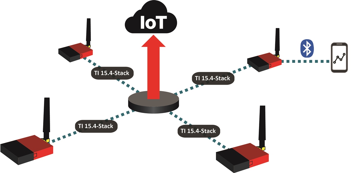
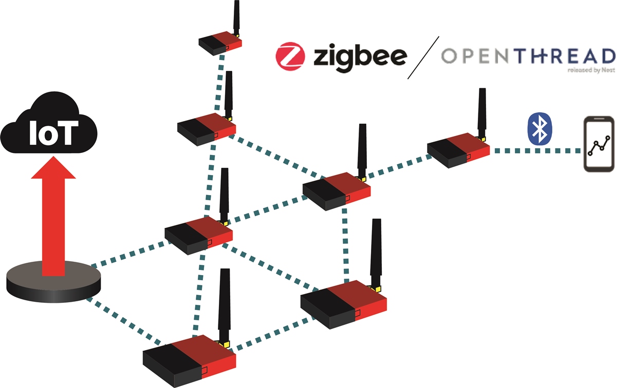
The LaunchPad SensorTag kit enables you to create low-power, battery-operated sensor nodes that can measure temperature, humidity, environmental brightness, Hall-effect, motion and more. Out-of-the-box connectivity and sensing capabilities allow you to easily collect sensor data in factory, building and industrial settings. The LaunchPad development kit aids developers in creating custom nodes or gateway solutions thanks to its unrestricted and open form factor. Both tools can help you quickly create a complete sensor network that is flexible, low power and secure. For example, you can create star topologies with Sub-1 GHz and/or Bluetooth Low Energy (shown in Figure 4) or create mesh topologies with Zigbee and OpenThread (shown in Figure 5).


Figure 4: Star topology created with the LaunchPad development kit and the LaunchPad SensorTag kit (LPSTK-CC1352R) hardware tools


Figure 5: Mesh network created with the LaunchPad development kit and the LaunchPad SensorTag kit (LPSTK-CC1352R) hardware tools


Full flexibility


The SimpleLink MCU platform includes the SimpleLink CC1352R multiprotocol and multiband MCU. With the SimpleLink CC1352R LaunchPad SensorTag kit (LPSTK-CC1352R), you can evaluate various connectivity frequencies and protocol stacks and seamlessly switch between multiple bands and protocols within your application. The multiband operation can offer seamless concurrent operation of Bluetooth Low Energy and Sub-1 GHz or Zigbee protocols. For example, you can use one SimpleLink CC1352R microcontroller device to offer both Bluetooth Low Energy connectivity and the long-range connectivity of Sub-1 GHz with the TI 15.4-Stack (Figure 6). You can also pair Bluetooth Low Energy connectivity with mesh protocols like Zigbee or Thread (Figure 7). The multiband, multiprotocol SimpleLink CC1352R MCU enables you to combine frequencies and protocols to create flexible connected sensor networks with a single MCU.


Figure 6. Bluetooth Low Energy + Sub-1 GHz with TI 15.4-Stack multiband operation


Figure 7. Bluetooth Low Energy + Zigbee/Thread stack multiprotocol operation


Software development tools


To complement the available SimpleLink hardware development tools, powerful and intuitive software tools and resources are available, from browser-based integrated development environments to graphical programming tools with the introduction of SysConfig, a unified software configuration tool. Code Composer Studio™ software is a powerful code editing, programming and debugging environment available for desktop and cloud operation. It provides the flexibility to develop on your desktop locally or within a web browser. SimpleLink SDK is a robust software development kit pre-integrated with peripheral drivers, connectivity stacks, libraries, RTOS kernel and more. In addition, it is backed by a quarterly release schedule introducing new features, improvements and optimizations. SysConfig (shown in Figure 8) is a new intuitive graphical configuration tool that is used to generate configuration code for the various SimpleLink SDK components. You can configure peripheral drivers, connectivity stacks and more with the help of a powerful graphical interface.

Figure 8. SysConfig graphical configuration tool


Additional resources


The LaunchPad development kit and the LaunchPad SensorTag kit (LPSTK-CC1352R) can work together to create flexible sensor networks with multiple connectivity options. Expedite time to market with the broad offering of TI tools and resources to meet your design needs. The SimpleLink MCU platform offers you flexible, easy-to-use hardware and software tools to help you create the next frontier of connected solutions.

What headlight resolution is high enough for symbol projection?

$
0
0

powertrain

This article was co-authored by Trevor Dowd.

Whether the application is your smartphone, your TV or your car’s headlights, having more pixels is usually better. These additional pixels increase the readability of small text and make small details visible on TVs.

New automotive headlight applications like adaptive driving beam (ADB) became available when technology advanced enough to allow 12 or more pixels per headlight. Now, DLP® technology enables carmakers to design cars with 1.3 million pixels per headlight. But what can you do with over 1 million pixels?

Automakers today need a lot of pixels in order to enable effective ADB, symbol projection and lane marking applications. However, not many technologies can accomplish all three applications today. One technology is TI DLP technology, which has developed a 0.55-inch diagonal digital micromirror device (DMD) designed with new advanced headlight applications in mind.

The DLP5531-Q1 is three times larger in active area than the first DMD designed for the automotive market (the DLP3030-Q1). The larger area supports three times more lumens than the DLP3030-Q1 (for a given illuminator source flux density) and triples achievable peak illuminance while using conventional LED light sources. The high temperature operating range includes operation at a die temperature of 105°C. The combination of higher temperature operation and a larger imager size helps support a broad headlight field of view (FOV).

Is 1.3 million pixels too many?

What applications require over 1 million pixels? On the surface, this amount of resolution seems like overkill, but in practice it’s actually not. To illustrate my point, let’s examine one example application: on-road augmented reality (AR)-style symbol projection.

To project images on a vertical surface such as a wall or garage door, resolution as low as 0.1 or 0.05 degrees per pixel is sufficient to create an interesting graphic symbol. Many demonstrations of these symbol projections exist in previous papers and conferences.

But what if the goal is not to display images on a wall, but rather to make the symbols appear to lie on the road’s surface, as if the symbol is painted on the road? If symbols were projected onto the road, automakers could design a visual communication system to help notify drivers of upcoming turns and better communicate with pedestrians.

For an image to appear as part of the road, one of the requirements is restricting the longitudinal length of the symbol on the road surface to a reasonable limit, say 2 to 3 m in length. Otherwise, the AR effect begins to get lost. Reducing the longitudinal length of the symbol reduces the vertical height of the symbol in angle space, which reduces the number of imager lines available to make the symbol.

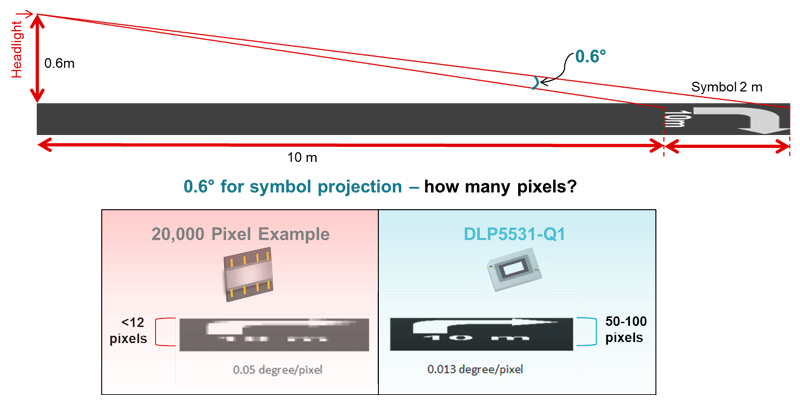
For example, when the imager’s maximum FOV is 7 degrees or more, the portion of the imager used for the symbol can be quite small in relation to the full FOV. The illustration in Figure 1 shows a 2-m-tall symbol at a relatively short distance of 10 m. The resulting height of the symbol in angle space is a mere 0.6 degrees. The calculation for the height of the symbol in angle space is shown in the top half of Figure 1.If the total vertical FOV is 7 degrees and the height of the image is the 0.6 degrees mentioned above, this means that the symbol must be constructed from only 8% to 10% of the available image vertical pixel lines. This 8% to 10% rapidly worsens if the distance from the car increases or the full FOV increases. If the image was projected to 20 m away from the car, the 2-m-tall image would occupy only about 0.16 degrees, or 2% of the available image vertical pixel lines.

 Pixel requirements for a 0.6° image height.

Figure 1: Pixel requirements for a 0.6° image height.

Figure 1 and the example above the figure shows respectable results with 0.013 degrees per pixel, but less-than-satisfactory results with 0.05 degrees per pixel. With just 0.05 degrees per pixel available, the 20,000-pixel system would require a taller symbol that covers several more meters of longitudinal road surface, which does not fit the AR definition. Even at a working distance of 10 m, we are able to see the value of having over one million pixels and are able to confirm that 1.3 million pixels are not too many. 

Modulation transfer function

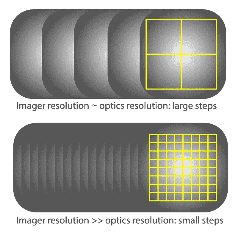
What is the advantage of having a rendering and imager resolution higher than the line pair resolving capability of the downstream projection optics? Line pair resolving capability is typically expressed as the modulation transfer function (MTF) of the projection optics. In systems with an optics MTF resolution lower than the imager’s pixel count limit, the optics set the minimum achievable feature size. But the object position adjustment resolution (and width/height step sizes above the minimum display size) is still governed by the imager resolution, as illustrated in Figure 2.

powertrain

Figure 2: Higher resolution gives precise control of motion and step size

The imager resolution affects how “smoothly” you can move and resize graphic objects such as masked areas around oncoming traffic. Using lower imager and rendering resolutions results in less natural motion, with discrete step sizes resulting in the appearance of motion judder. This judder effect is irrespective of the optical blurring caused by the limited MTF of the projection lens.

Conclusion

For a system using the DLP5531-Q1 0.55-in DMD operating in 1152-by-576 mode (half of native resolution) and a 7.5-degree full vertical FOV, the resulting vertical resolution is 0.013 degrees per pixel. For vertical FOV sizes significantly greater than 7.5 degrees, the 1152-by-1152 operating mode (native resolution) of the DMD is available and can double the effective vertical line resolution to maintain this level of performance. So even if you use the DMD for the entire traditional high-beam FOV plus symbol area, the 0.55-in DMD has the resolution required for on-road AR symbols.

Additional resources


Get more out of your power supply with port power management

$
0
0

With the publication of the new Institute of Electrical and Electronics Engineers 802.3bt standard, the power range of Power over Ethernet (PoE) loads continues to expand. If you are designing systems that provide PoE, this presents a challenge. You may need to provide 5 W of power to a low-end Internet Protocol camera or 70 W to a high-end wireless access point (WAP). An enterprise switch with 48 ports that can simultaneously support 90 W on all ports would require a 4.3-kW supply.

You probably want to enable the full functionality of the high-end WAP, but do you really want to pay for the giant power supply? Knowing the typical use case of your system, you can choose a smaller power supply that would be sufficient in most situations. But, how do you prevent the supply from overloading in the rare event that all loads draw full power?

Port power management (PPM) algorithms can come to your rescue. When a new device is plugged in, the system will only turn the device on if there is enough remaining power. A system that supports priority and exceeds its power budget will actually shut down a lower-priority load when a higher-priority load is plugged in.

At a high level, PPM is a simple concept, but it can have multiple flavors, and its implementation can be tricky. Typically, there are multiple power sourcing equipment (PSE) devices, thus requiring a central microcontroller (MCU) to manage the system. Also, the system could have slots for multiple power supplies, which can get plugged in or unplugged during operation.

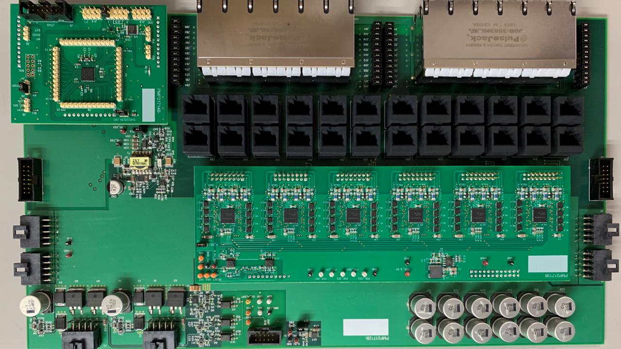
TI’s FirmPSE ecosystem can give you a huge head start in implementing PPM in your end equipment by removing the burden of writing low-level code to control the PSEs. Figure 1 shows the evaluation board of TI’s FirmPSE, which is implemented using an MSP430™ MCU and TPS23881 PSE. TI provides a binary image that you can load directly into the MSP430F5234. You will need to write code that interfaces between the host central processing unit (CPU) and the MSP430F5234 to configure the system and monitor the port status.

 Evaluation board of TI’s FirmPSE ecosystem

Figure 1: Evaluation board of TI’s FirmPSE ecosystem

TI’s ecosystem features:

  • Orderable TI designs with twenty-four 90-W PoE ports.
  • A user’s guide.
  • A binary image that can be loaded directly to the MCU.
  • A host interface document defining the interface between the MSP430F5234 and host CPU.
  • A graphical user interface to configure the binary image and to evaluate monitor port status’s of the FirmPSE system.


To learn more about PPM and ways to reduce your power supply consider watching our FirmPSE system firmware GUI offline mode or online mode training videos.

Why current and magnetic sensing matters for wireless earbud design

$
0
0

Wireless earbuds have infiltrated the electronics market in recent years. Users can now walk away from their streaming devices without the fear of being yanked back by a caught wire. True wireless earbuds are Bluetooth®-based wireless earbuds that have their left and right channels separated into individual housings. And while this innovation has freed consumers from having to be connected to their phones by a wire, it has also presented a host of new design challenges for earbud manufacturers.

To maximize battery life and support long battery runtime, it’s important to ensure an efficient charge with the earbuds seated properly in their charging case. Magnetic sensors helpensure proper earbud seating because they use magnets to detect fine object movements. Commonly, using current-sense amplifiers for earbud charging and Hall-effect switches for wireless charging cases support maximium battery charge and battery life for these applications.

Designing with current-sense amplifiers

The batteries in wireless earbuds are often in the sub 100-mAh range. Therefore, better current measurement is necessary in order to protect and accurately charge these smaller-capacity cells. Traditional battery chargers and gauges do an excellent job of monitoring larger currents for batteries like those in a charging case, but often do not fare well at super-low currents.

Dedicated current-sense amplifiers are more accurate when measuring small currents. If you already have a microcontroller (MCU) or power-management integrated circuit (PMIC) in your design, you can use the output of these amplifiers to monitor and gauge battery use times and lifetimes based on algorithms written in the MCU or PMIC.Figure 1 shows a battery fuel gauge with an external current-sense amplifier and controller.


Figure 1: Battery fuel gauging with an external current-sense amplifier and controller

Placing two small-size current-sense amplifiers like the INA216 in a wireless earbud charging case will enable highly accurate charging current measurements. Alternatively, if solution size is a priority, using a single dual-channel-capable current-sense amplifier like the INA2180 is recommended.

If accuracy is less important, and assuming an equal current division, one current sensor can monitor charging in both earbuds. Placing bidirectional-capable current-sense amplifiers like the INA191 or INA210 in the earbuds themselves will enable both charging and gauging functionalities. Regardless of which topology you choose, these devices can also enable better battery protection, as even small changes in current can affect battery lifetimes.

Designing with Hall-effect sensors

A new feature of wireless earbuds is lid and charge detection within their companion charging cases. Charging cases must be able to detect the position of the lid and be able to detect the presence of the earbuds inside the case for charging. Other sensor technologies may not have the ability or sensitivity to discern these things correctly in a cost-effective manner, so choosing the right sensor is crucial. Figure 2 shows wireless earbud sensor placement.


Figure 2: Wireless earbud sensor placement and use

Hall-effect sensors work well for charging case lid and earbud charge detection. Magnets are already used to clasp charging case lids shut, so using a magnetic sensing solution for lid detection in the form of Hall-effect switches is an obvious solution that requires no extra parts. In addition, placing magnets in the earbuds themselves enables a robust means of detecting whether the earbuds are present inside their charging case. Knowing whether the earbuds are in or out of the case will allow Bluetooth auto-connect when the earbuds are removed, or charge detection when they are inside the case.

Choosing the right digital Hall-effect sensor is important, and features such as low frequency and low. power make the DRV5032 a good fit. For Hall-effect sensor applications in earbuds, providing magnet detection information five times per second is more than enough. This frequency allows you to use the DRV5032’s low-power option, which consumes only about 0.5 µA and does not place a significant drain on the device’s battery.

Determining state of charge and charging case lid detection are both critically important to earbuds with their small-capacity batteries and wireless connectivity. Current-sense amplifiers and Hall-effect sensors provide a solution for those struggling to design around these new features and challenges.

Additional resources


New logic family enables noise-tolerant and lower-power system designs

$
0
0

Electrical noise can be a designer’s worst nightmare, leading to unexpected system behavior or even failure that is very difficult to trace. In traditional High-speed complementary metal-oxide semiconductor (CMOS) logic, noise can lead to signal oscillation, resulting in higher current consumption and even producing signal errors. These errors can ultimately lead to a system malfunction, requiring more engineering effort and possibly a design change.

Many design engineers combat signal noise by using external Schmitt-trigger input-based logic buffers. Schmitt triggers eliminate oscillation by using two thresholds for signal transitions, which clean up both slow and noisy signal edges and prevent noise from propagating down the signal chain and resulting in signaling errors. The net result is better system robustness and performance. Figure 1 shows the benefits of Schmitt triggers.

Figure 1: Benefits of Schmitt-trigger inputs

The logic devices used by a system designer can play a critical role in enabling designs that are less susceptible to noise. TI’s HCS logic family, which uses its latest 300-mm wafer process, supports solutions for a diverse set of markets, from industrial and automotive to personal electronics. The HCS logic family provides the building logic blocks for next-generation systems with superior robustness, power efficiency and performance.

High-speed complementary metal-oxide semiconductor (HCMOS) multi-gate logic functions have been in use for several decades by the electronics industry. The HCS family is an update to the HC logic family. HCS logic modernizes multi-gate logic functions to meet the needs and demands on today’s system designers. Each HCS logic part, numbered SN74HCSxx, is a pin-to-pin drop-in replacement for existing HC logic parts, with no need to update designs or change development tools.

Selecting a logic family today for noise-sensitive, low-power and rugged applications in markets such as automotive and industrial is complicated. Today, design engineers have to integrate a disparate set of components to create a system that balances power consumption, performance, reliability and cost.

The HCS family simplifies logic device selection and product design by providing an entire family of multi-gate logic functions that address noise and/or power concerns, integrating Schmitt-trigger capability on every data input. Schmitt-trigger input functionality directly benefits a wide range of applications. Applications such as advanced driver assistance systems and factory process controllers are just a few examples of the systems that can benefit from HCS logic devices. The integrated Schmitt triggers help improve noise immunity and glitch-free operation in systems without the need for external signal conditioning; see Figure 2. The HCS family was designed with automotive applications in mind and is the first TI logic family to launch with a complete line of both commercial- and automotive-grade parts.

Figure 2: Comparing traditional HC logic implementation vs. HCS logic

Built for efficiency and robustness

The HCS family improves efficiency not just by eliminating the need for external signal buffering but also by directly reducing power requirements for a system’s logic implementation. Quiescent current (IQ) for an HCS part is just 2 μA, compared to 20 μA for comparable HC logic. Each device in the 2-V to 6-V HCS family consumes 95% less power than its equivalent HC logic function, making HCS logic devices much more suitable for battery-powered designs.

Extremely low power consumption is just the beginning. The HCS family also minimizes delays, with a 40% improvement in propagation delay, while improving current drive by 50% over HC equivalent devices. This means that designers do not have to compromise on performance in order achieve lower-power system logic implementations.

Reliable support and design-centric development collateral

Choosing a logic family is about more than just selecting a bundle of devices. To help you get up to speed on the HCS logic functions, TI has produced application notes, training materials and technical articles. In addition, the HCS family is backed by a dedicated TI logic application support to help you reduce design cycles, meet design budgets and find an easier path to market for your final product.

HCS logic functions are drop-in replacements for equivalent HC logic functions and will be available in common package types (small outline and thin shrink small outline packages), eliminating any learning curve to introduce HCS devices into your designs.

Conclusion

The new HCS family incorporates many of the features and capabilities that designers have demanded, such as Automotive Electronics Council-Q100 qualification, dramatically lower power, noise tolerance and robust signal performance, all while maintaining backward compatibility.

The HCS logic family is more than just a new logic family. It's a way to improve the robustness of your designs.

Additional resources

VIDEO: Building security with glass break detection

$
0
0

(Please visit the site to view this video)

Systems design engineer, Brian, shows us a really cool glass break and fire/carbon monoxide (CO) alarm detection demo for a building security system using the SimpleLink™ CC1312 wireless MCU. This board has the capabilities to seamlessly switch between a glass break detector and a fire/CO alarm detector with the flip of a switch. The detection algorithms leverage Fourier Transforms, zero point axis crossing for the glass break detector, as well as temporal pattern detection for the fire and CO alarm detection. Detection can either be initiated by the sound pressure level (comparator based) or frequency spectrum based (ADC Directly). Check it out!

Extending 2.4 GHz without compromising performance in a connected world

$
0
0


In a world where just about everything is connected, design engineers are always looking for new ways to enable wireless technology without compromising range or performance. Many thermostats or heating, ventilation and air-conditioning (HVAC) controllers have built-in wireless technology, enabling homeowners to communicate with their smart home by simply using their cellphone.


The same principle applies in the industrial space, where business owners or factory operators want the ability to continuously monitor the health and status of their HVAC and other connected systems. This can be achieved using a long-range wireless link rather than expensive and inflexible wired deployments. The 2.4 GHz band uses shorter waves and typically has a shorter transmission range unlike Sub-1 GHz technology.


Achieving long range

One way to extend range in a 2.4 GHz wireless application is to use a power amplifier (PA) to increase the power at which that the system is transmitting, which in return increases the application’s total link budget. To put this in perspective, each +6-dBm increase in link budget doubles the total range of the system in free-space at ideal conditions.


The SimpleLink™ CC2652P microcontroller (MCU) provides an integrated +20-dBm PA, which approximately quadruples the range at 2.4 GHz compared to solutions currently available on the market without an integrated PA which makes it a good fit for industrial settings. This enables the deployment of sensors in remote locations and decreases the number of gateways/routers in your network.


Flexible design with wireless multiprotocol

Bluetooth-connected devices can extend their connectivity to communicate with and control the latest smart devices but may no longer be sufficient in this age. Many new applications like Thermostats now runs on multiple wireless protocol stacks concurrently to enable support to communicate with cellphones and various smart home devices at the same time.


The SimpleLink CC2652P MCU supports Bluetooth® 5.1 Low Energy, Zigbee, Thread, TI SimpleLink 15.4 (2.4 GHz) and additional simultaneous protocol combinations through a dynamic multiprotocol manager found in the SimpleLink™ CC13x2 and CC26x2 software development kitwithout the need for additional hardware. The ability to use various combinations of wireless technologies to address system needs can help eliminate wires and enable more flexible system deployments.


Low power is essential

Extending a battery-operated device like a wireless temperature and humidity sensor can be vital when you want to ensure years of operation versus just a few months. This example of battery-powered wireless sensor periodically samples and transmits data. A long battery life for such a sensor is especially important in cases where the battery is nonreplaceable or is located in an inaccessible location.


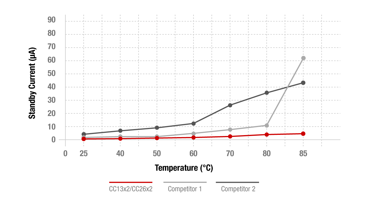
The CC2652P MCU is optimized to power off of a single coin-cell battery with a peak transmission current of 22 mA at +10 dBm. The CC2652P MCU also offers a low-power integrated PA capable of achieving up to +20-dBm output (Tx = 85 mA at 2.4 GHz). Additionally, the CC2652P consumes only 5 µA of current at 85°C for low-power industrial applications.


The CC2652P MCU ultra-low-power sensor controller engine is a programmable CPU to create smart sensing applications. The sensor controller engine consumes about 1 µA of system current for a 1-Hz analog-to-digital converter sampling application.


As you can see in Figure 1, all of these factors combine to enable you to meet power-consumption requirements without sacrificing performance across the industrial temperature range.


Figure 1: SimpleLink MCU diagram showing standby current consumption


Conclusion

As you can see, it is possible to extend range while maintaining solid performance and low power in your wireless design. Wires are expensive, inflexible and in many instances antiquated in our connected world. The SimpleLink CC2652P MCU can help you jump-start your design and achieve a flexible solution with both low power and long range.

Sequencing and powering FPGAs in radar and other defense applications

$
0
0

Aerospace and defense applications, from ruggedized communications to radar to avionics equipment, require intelligent power with accurate voltage regulation, high power density, high efficiency and comprehensive system diagnostics for high reliability.


More and more aerospace and defense applications are using faster, higher-performance processors and field-programmable gate arrays (FPGAs). As shown in Figure 1, radar requires not just a DC/DC converter for the digital signal processor (DSP), FPGA and input/output (I/O) rails, but also a sequencer to provide accurate sequencing for power-up and power-down scenarios.

Figure 1: Radar block diagram

Why do you need to sequence the power rails?

Improperly sequenced power rails present several risks to the power supply, including compromised reliability (which can lead to device failures), stress on the integrated circuit, reduced application life and immediate faults, which relate to excessive voltage differentials and current inflow. Figure 2 shows a typical power-sequencing diagram.

Figure 2: Power-sequencing diagram


As shown in Figure 3, there are three types of sequencing schemes: sequential, ratiometric and simultaneous:

  • Sequential is when two or more voltage rails power up or power down in sequence at different slew rates and with different final values.

  • Ratiometric is when two or more voltage rails power up or power down at the same time at different slew rates and with different final values.

  • Simultaneous is when two or more voltage rails power up or power down at the same time with the same slew rate but different final values.


Figure 3: Types of voltage rail sequencing


The ability to address all of these sequencing schemes but also monitor the power-supply rails and report system warnings and faults with flexibility and ease of use is critical in order to prevent runaway issues like overcurrent and overtemperature.


The UCD90320Uis TI’s newest 32-channel PMBus sequencer which can be programmed and reconfigured through its onboard nonvolatile memory for a wide range of sequencing scenarios through the Fusion Digital Power™ Designer graphical user interface, as shown in Figure 4.


Figure 4: Voltage rail sequence timing configuration window in Fusion Digital Power Designer


Dealing with ionizing radiation exposure


In radar and other defense applications, there may be instances of ionizing radiation exposure. When this happens, the failure-in-time (FIT) rate can increase; that is, the probability of failure can increase. A typical instance of ionizing radiation failures in semiconductors is a single-event upset (SEU). An SEU is caused by ionizing radiation strikes that discharge the charge in storage elements such as configuration memory cells, user memory and registers, resulting in a bit flip as shown in Figure 5. The change caused by an SEU is considered “soft” because the circuit/device itself is not permanently damaged by the radiation. If a new data is written to the bit, the device will store the new data correctly.


Figure 5: An ionizing radiation SEU affecting a memory cell


In terrestrial applications, the two radiation sources of concern are alpha particles emitted from package impurities and high-energy neutrons caused by the interaction of cosmic rays with the earth’s atmosphere. Studies conducted over the last 20 years have led to high-purity package materials (ultra-low alpha [ULA]), which can minimize SEU effects caused by alpha particle radiation. Unavoidable atmospheric neutrons remain the primary cause of SEU effects today.


The UCD90320U uses a compact 0.8-mm pitch ball-grid array package with a ULA mold compound to reduce the soft errors caused by ionizing alpha particles. This sequencer/monitor also has the ability to scan the user-configuration static random access memory to detect SEUs. Both ULA and SEU detection features provide higher reliability for radar and other defense applications. Based on actual customer results, the FIT rate dropped to 10 with the UCD90320U in the ULA package, versus a FIT rate of 1,344 with the non-ULA package.


Achieving effective voltage regulation


After successfully sequencing the FPGA rails, the FPGA core rail is the most critical in terms of voltage regulation, power density, thermal performance and efficiency. Some of the latest FPGAs require a total tolerance of ±2% DC plus AC (AC = load transient), which makes voltage regulator design challenging. Table 1 lists typical high-current FPGA core and I/O rail design specifications.


PARAMETER

SPECIFICATIONS

Input supply

12 V, ±5%

Switching frequency

500 kHz

Power stages

CSD95490Q5MC

Core rail

Nominal output voltage

0.9 V

DC+AC tolerance

±2%

Max output current

120 A

DC load line

-           

Max load step

30 A at 100 A/μs

Number of phases

3

COUT, BULK

12x 470 μF, 2.5 V, 3 mΩ

COUT, MLCC

22x 220 μF, 4 V, X5R

I/O rail

Nominal output voltage

0.9 V

DC+AC tolerance

±2%

Max output current

20 A

DC load line

-

Max load step

10 A at 100 A/μs

Number of phases

1

COUT, BULK

8x 470 μF, 2.5 V, 3 mΩ

COUT, MLCC

8x 220 μF, 4 V, X5R


Table  1: High-current FPGA core and I/O rail power specifications

Radar and other defense equipment customers typically prefer power modules for the ease of use and maintenance-free benefit. For an FPGA requiring 120 A of output current, an equivalent discrete multiphase buck voltage regulator solution requires 66 discrete components and hundreds of hours of design, layout, lab testing, prototyping, reliability and final testing. The design will also be subjected to electromagnetic compatibility testing, and for defense applications, shock and vibration testing as well.

For the highest-performance FPGA, TI’s TPSM831D31120-A plus 40-A dual-output PMBus buck module can help designers meet ±2% DC and AC tolerance specifications at high power densities, with 243 W of output power in 720 mm2 of printed circuit board area.


Employing our proprietary DCAP+™ control mode, the TPSM831D31 can reduce the output capacitor count, including the number of multilayer ceramic capacitors required to maintain output voltage regulation during severe load transients. The TPMS831D31 can power both the FPGA core and I/O rails, as shown in Figure 6.

Figure 6: TPSM831D31 application circuit

If you are designing a radar or any other defense equipment using high-current FPGAs and your design priorities are comprehensive sequencing, monitoring, ease of use and high power density for your FPGA DC/DC converter, consider using reconfigurable PMBus sequencers such as the UCD90320U and high-performance modules such as the TPSM831D31.


Additional resources:


How stepper motors improve noise and efficiency in automotive system design

$
0
0

Stepper motors are popular in vehicle lighting systems for headlight leveling and steering. As automakers transition to quieter electric vehicles, noise reduction in these systems becomes more important and requires a well-tuned stepper motor with the ability to detect stall conditions. This is particularly true for automotive lighting systems, where the motor needs to detect the “end of travel” for headlights.

Tuning a stepper motor system is time-consuming and involves trade-offs related to the supply voltage, motor winding inductance and resistance. Smart tuning can help engineers overcome these trade-offs for ripple control by automatically selecting the optimal current regulation scheme and eliminating the need for tuning. Additionally, back-electromotive force (EMF) sensing methods provide a stall detection function to reduce the noise at endstops. It is important to consider electromagnetic interference (EMI) when there are long cables from the electronics to the lightning assemblies.

In automotive stepper motor applications such as headlights and head-up displays (HUDs), the system needs to know if the motor is stalled or if the motor has reached “end of travel” to avoid overdriving the motor, which can result in power loss or mechanical noise.

To help detect stall conditions more accurately, TI has implemented a new current-regulation scheme in our DRV8889-Q1 motor driver. Traditional schemes use fixed off-time regulation. But smart tuning for ripple control controls the current between a peak value (ITRIP) and a lower level (IVALLEY), resulting in a variable pulse-width modulation (PWM) off time that can be monitored.

A stall detection algorithm compares the back-EMF between the rising and falling current quadrants by monitoring the PWM off time and generates a value represented by the 8-bit register TRQ_COUNT. The comparison is done in such a way that the TRQ_COUNT value is practically independent of the motor current, motor winding resistance, ambient temperature and supply voltage. For a lightly loaded motor, the TRQ_COUNT will be a nonzero value, as the back-EMF is different between t1 and t2, as shown in Figure 1. If the motor approaches a stall condition, TRQ_COUNT will approach zero, as the back-EMF is the same between the two quadrants. After detecting a stall condition, the system controller can stop sending the step signal and reduce the winding current, which will in turn reduce audible system noise and power consumption.


Figure 1: Motor back-EMF vs. winding current

As cable harnesses become longer in automotive vehicles, it is important to consider EMI mitigation techniques in motor drivers. Stepper motor drivers use a PWM technique to regulate the output current. There are two switching power converter EMI control methods that you can apply to motor drive systems.

For a switching converter, the slew rate is related to the switching noise roll-off frequency. The 40-dB/dec roll-off frequency is inversely proportional to the slew rate of the driver. By changing the slew rate from 100 V/µs to 10 V/µs, the 40 dB/dec switching noise roll-off frequency will be one decade earlier, which will push the noise down 40 dB and significantly improve the EMI performance, as shown in Figure 2. The DRV8889-Q1 has four slew-rate settings that are configurable through a serial interface.


Figure 2: EMI noise vs. switching converter slew rate

Switching converter EMI noise is a function of the converter’s switching frequency and its harmonics. The second method is a spread-spectrum technique that modulates the switching frequency and dithers the PWM clock, which distributes the noise energy to other frequencies and lowers the peak frequency energy. Figure 3 shows the EMI test result with the spread-spectrum clocking function enabled and disabled on the DRV8889-Q1 evaluation module.


Figure 3: EMI noise vs. spread spectrum with 12 VM; a 100-V/µs slew rate; 1/32 microstep; 1,000 step pulses per second; 1-A full scale current and ripple control dynamic decay: enabled (a); and disabled (b)

The DRV8889-Q1 stepper motor driver offers three main benefits when using stepper motors in automotive, HUD, engine and motorbike applications. The smart tuning for ripple control algorithm automatically adjusts the current regulation behavior to minimize ripple and noise in the system. The algorithm also gives you a value proportional to back-EMF that you can use to determine when a headlight has hit an endstop and minimize the rattling noise that can result from over-travel. Finally, EMI countermeasures have been incorporated in the DRV8889-Q1 to reduce EMI.

Viewing all 4543 articles
Browse latest View live


<script src="https://jsc.adskeeper.com/r/s/rssing.com.1596347.js" async> </script>