Quantcast
Channel: TI E2E support forums
Viewing all 4543 articles
Browse latest View live

Understanding tamper detection sensors

$
0
0

Many systems require a method to detect tampering. In some cases, that could mean that the door of a product has been opened. In other cases, it could mean that a seal on a device has been breached, or that an external element is affecting measurement precision. Device tampering can have many negative impacts, including unexpected changes in functionality, a safety risk to humans, security breaches or ruined devices. The good news is that many different kinds of sensors can assist in the effectiveness of tamper detection.

In this technical article, I will compare several tamper detection methods in order to help you choose the right option for your next design. It is possible to implement tamper detection in constrained applications when you need to minimize space and power consumption, such as in battery-powered or other applications where the standby power must stay below a certain level. Sensors from TI, for example, have been optimized to be small in device size and low in quiescent current draw.

Do you need tamper detection in your design?

Tamper detection is appropriate when there is:

  • A safety-critical need to shut off a portion of a product if opened, such as a smart lock or a high-voltage power supply.
  • Any possibility that a device will be damaged once tampered with, such as products submerged in water or other harsh environments.
  • The potential that a user may tamper with a device to alter its functionality, such as an electricity meter.

Let’s look at four different tamper detection sensor technologies.

How to select the right sensor for tamper detection

Hall-effect switches detect the type of tampering where a case is opened by mounting a magnet to the door of the device; see the Magnetic Tamper Detection Using Low-Power Hall-Effect Sensors Reference Design shown in Figure 1. Once the door moves away from the sensor, the magnetic flux is no longer present and the sensor can then determine whether the case has been opened. Hall-effect sensors have the advantage of being very low in power consumption; for example, the DRV5032 has an average current draw of 0.54 µA.

In systems where case tampering is important, Hall-effect linear devices can also determine the strength of external magnetic fields not present during normal operation. In some parts of the world, disabling a system with large magnetic fields produced by strong magnets does occur. A linear device such as the DRV5055 can detect whether a large magnet is in close proximity to the system and alert the service provider. In some cases, multidimensional axes of detection offer a more robust solution.


Figure 1: The magnetic tamper detection reference design with an external tamper magnet

Inductive sensors, in conjunction with a printed circuit board (PCB) coil and a metallic object, can detect the changing inductance of a coil and thus are a good fit for detecting tampering where a case is opened. An inductive sensor used for this type of tamper detection, as illustrated in Figure 2, has the advantage of being able to perform detection with the target being a metal object, such as a safe door. But because the PCB must have sufficient space for the coil, this is the most complex of the four sensor methods. If you choose this method, make sure to consult the additional resources at the end of this article.


Figure 2: LDC0851 inductive sensor block diagram

Humidity sensors, as shown in Figures 3 and 4, are able to measure relative humidity and temperature. This type of sensing can detect a broken seal or leak tamper. For devices that are sealed to protect against harsh environments, a humidity sensor is an effective way to control the environment inside the device. As soon as the humidity level rises, the sensor will detect the broken seal and take corrective action. Humidity sensors are particularly useful for underwater devices. A humidity-based solution does not require any external elements; however, it is more expensive than other sensor technologies.


Figure 3: HDC2080 humidity sensor package


Figure 4: HDC2080 block diagram

Ambient light sensors, as shown in Figures 5 and 6, can determine a change in illumination and can sense an increased optical response during a broken seal or opened case. For a design with a known amount of light at the PCB, an ambient light sensor offers an easy way to implement tamper detection. Once the light level rises, the end equipment has entered an unexpected state. One example is a money drawer in a cash register. If the register is closed and light enters unexpectedly, that indicates a tampering scenario.


Figure 5: OPT3002 ambient light sensor package


Figure 6: OPT3002 ambient light sensor block diagram

Table 1 is a high-level comparison of the four tamper detection sensor technologies.

Sensor TypeCostExternal elementsType of tamperingEnvironmental needsDetectabilityPower consumptionDesign complexityKey products and size

Hall-effect sensors

Low

MagnetCase open, system tamperingAccess to two pieces of the caseMagnetic field

Switch: 0.54 µA at 5Hz

Linear: 6 mA

Medium

DRV5032 1.54 mm2

DRV5055 3.80 mm2

Inductive sensorsMediumPCB coil and metallic objectCase open, impervious to magnetic fieldsAccess to place the PCB coil; needs metal to senseConductive targets (such as copper)2 µA to 4 µA at 1 HzHighest

LDC0851    4 mm2

Humidity sensorsHighNoneBroken sealNoneChange in humidity550 nA at 1 HzLowHDC2080    9mm2
Ambient light sensorsMedium    NoneBroken seal, case openNeeds to have light levels change when case opensAny light (broad spectrum to include infrared)1.8 µALowOPT3002    4mm2

Table 1: Sensor comparison

Each of the four different methods leverages low-power and small-size sensors to implement tamper detection. Which method will work best for your system?

Additional resources


Why the future of automation is being propelled by innovation at the edge

$
0
0

 Sameer Wasson discusses the future of automation and intelligence at the edge.


The future of intelligent machines rests on innovation at the edge – the embedded technology that enables real-time sensing and processing for more dynamic decision-making.

Automation that used to be preprogrammed and structured has evolved so that machines now understand in real time what’s happening in their environment and can react to it intelligently, safely, securely and autonomously. The technology that enables this is machine learning – a subset of artificial intelligence – and it’s transforming machines that were once line cooks into chefs. But they’re not quite master chefs.

As signal processing technology has evolved and added more machine learning features along the way, we have opened the door for advances in vehicle occupancy detection, intuitive human-machine interaction and more without needing to rely on cloud processing every time.


 Learn how we’re bringing the next evolution of machine learning to the edge.

Auto and DL demo

For example, edge intelligence in your future vehicle will be able to sense an object nearby and classify it as a pedestrian. The machine learns from this experience in real time and evaluates data, such as response time between object detection to vehicle action, to improve over time.

And when you park it in the garage that evening, it connects to the cloud and shares that knowledge with the entire connected fleet.


Now take that technology into a field of corn, where planters are programmed to sow seeds about every six inches. Since the ground can be inconsistent, sometimes seeds don’t do well – they might need to be planted deeper or spaced farther apart. Embedded intelligence enables the planter to analyze the soil for moisture, nutrients and other data before a seed is planted. It can predict how many seeds will successfully mature, and the data can be uploaded to the cloud so that farmers can forecast yields.

Or imagine your future shopping experience: in stores that are on the cutting edge of retail automation, customers scan their phone as they walk in. A combination of cameras and in-shelf sensors tally up the items put into their basket, automatically billing customers when they leave.

Currently, this requires sending streams of data from potentially hundreds of thousands of stores up to the cloud for processing by machine learning algorithms. That's an enormous amount of data, which can present significant challenges. With TI mmWave sensors and processors – highly intelligent sensors that integrate precise, real-time decision-making and processing on a single chip – that data can be processed in the store itself to reduce that load.

Eventually, the boundary between the edge and the cloud will start to get very interesting. How rapidly the technology can prioritize which data to send to the cloud quickly, repeatedly and consistently – and receive actionable information back – will be the next problem to solve.

As we find solutions at the edge for automation, our everyday machines will continue to make our lives more convenient, efficient and safer.

Sameer Wasson is vice president and general manager of our Processors business unit.

3 tips when designing a power stage for servo and AC drives

$
0
0

The Industry 4.0 revolution enables the capture and analysis of data about various machines, resulting in faster, more flexible, more reliable and more efficient processes to produce higher-quality goods at lower costs. Industry 4.0 does create some challenges at the system level, however, for engineers designing power supplies with DC/DC step-down regulators. These challenges include the need to improve reliability, enhance heavy load efficiency to minimize thermal dissipation, and provide a faster transient response to achieve a smaller output capacitance.

1. Think about wide input voltage and high current.

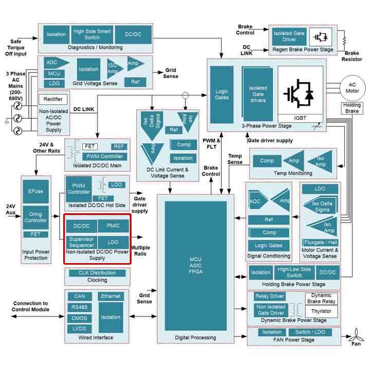
Figure 1 shows a simplified power architecture for a servo drive power stage, which is powered by a 24-VDC auxiliary power source. The 24-V can also be generated by the DC Bus voltage by using an isolated power supply. The first stage is the field input protection circuit; the second stage is the nonisolated DC/DC field power supply.

Figure 1: Servo drive module power architecture

The power supply typically needs to support 36-V or even up to 60-V operation and requires DC/DC converters rated for higher current (>1 A) to protect against unexpected power surges caused by long cables, hot plugs and ringing – familiar scenarios for engineers designing power solutions for the industrial world. As such, when designing a power supply for industrial applications like servo or AC drives, consider step-down converters that offer a wide input voltage.

The LMR36520 has a transient tolerance as high as 70 V, which helps protect against overvoltages and meets the surge immunity requirements of International Electrotechnical Commission 61000-4-5. If 36 VIN is acceptable for your application, you can pick converters based on the required load conditions. The LMR33610, LMR33620, LMR33630 and LMR33640 enable you to reuse most of your layout, significantly simplifying your system-level schematic and layout design and reducing R&D efforts.

2. Choose devices with fast transient response.

Because of their ruggedness, AC drives can be used to control the induction motors used in processing plants. Besides that, AC drives control the speed of an AC motor by varying the output voltage and frequency through a sophisticated microcontroller (MCU)-controlled electronics device. Figure 2 shows the power-supply design for a safety MCU in AC drive system. This safety power supply (3.3 V) is designed to power up the safety MCU and other loads. The power supply can also be used for servo drives besides the AC drive.

Figure 2: Power-supply design for servo drive system

Higher supply voltage can affect the normal operation of an MCU or even damage it, when the supply voltage is higher than the MCU’s absolute maximum supply voltage rating. Lower supply voltage, in turn, can negatively impact MCU’s reset circuits’ or peripheral circuits’ (such as general purpose input/output -GPIO) drive capability, preventing them from operating normally. Thus, when using a power supply to power both an MCU and another dynamic load, consider devices that offer fast transient performance. During the load transient, those devices will have lower overshoot/undershoot voltage at the output side, without impacting the operation of the MCU. Fast transient performance reduces the pressure on the MCU and secondary point of load regulators, improving system robustness and potentially eliminating the need for protection devices such as clamping diodes.

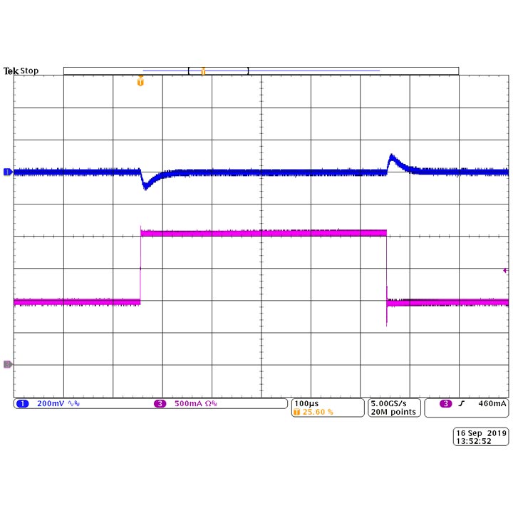
Figure 3 shows the load transient and switching waveforms of the LMR36520. When the load increases from 1 A to 2 A at a 1-A/µs slew rate, there is only 100 mV of overshoot and undershoot.

Figure 3: LMR36520 load transient

3. Don’t forget about ground protection.

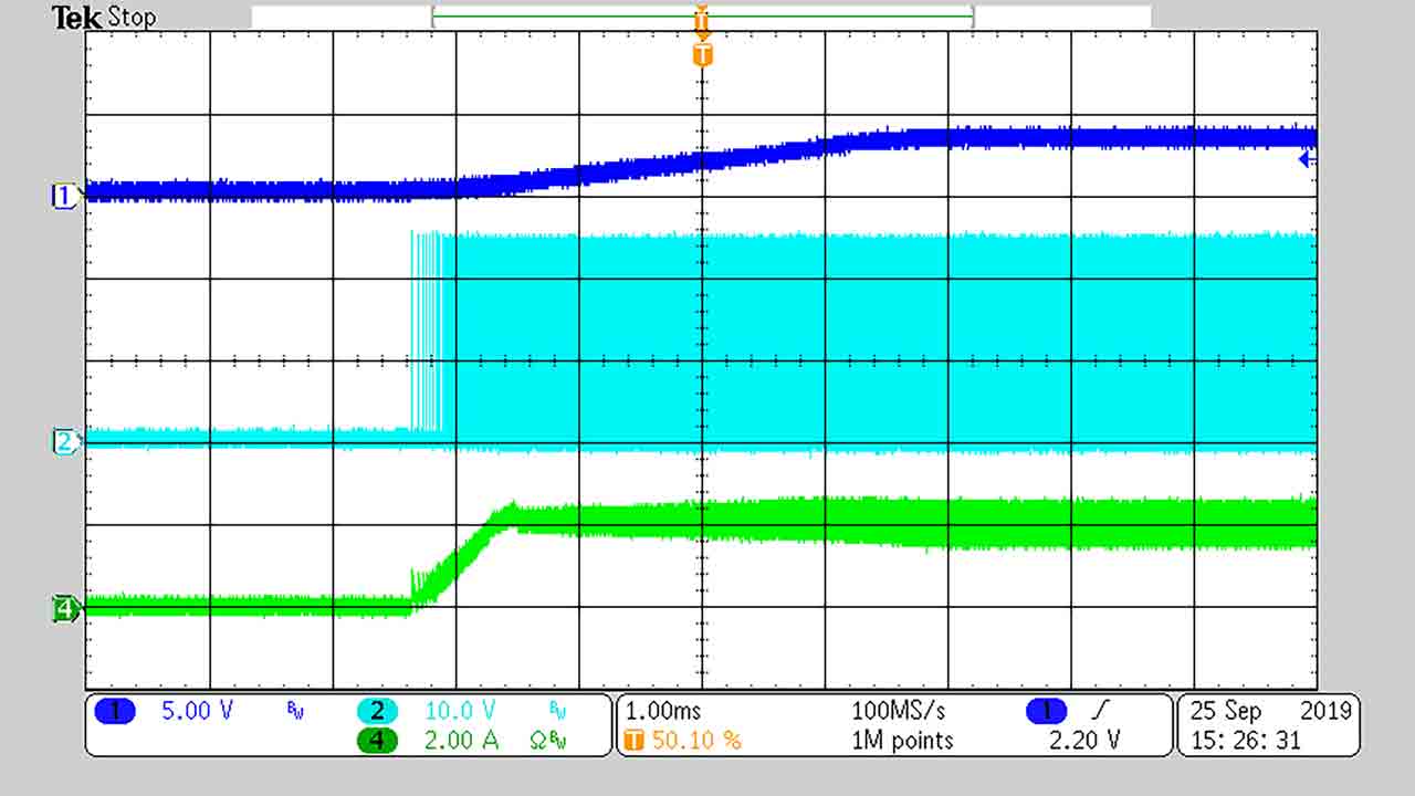
The power supply will also need output-short-to-ground protection. The power-supply output from Figure 2 also powers buffers and communication interfaces. In a real-life industrial environment, an operator might forget to turn off the power when changing some component, which could cause the power supply’s output (3.3 V or 5 V, depending on the MCU) to short to ground. When a 3.3-V or 5-V load is shorted to ground and released, you don’t want to see overshoot at the 3.3-V or 5-V rail because that might damage the MCU, which usually has an absolute maximum operation input voltage of 6 V. To prevent overshoot, look for buck converters with properly designed hiccup-protection features. As Figure 4 shows, the LMR36520 has good output-short-to-ground recovery protection.


Figure 4: LMR36520 short-to-ground waveform

Conclusion

When designing the power supply for a servo and AC drive, think through the potential impact of your design. A wide input voltage, higher output current, fast transient performance and good short-to-ground protection are the key factors you should consider during development.

Additional resources

Why signal isolation matters in 48-V HEV/EV systems

$
0
0

One of the key differences between conventional internal combustion engine vehicles and hybrid electric vehicles (HEVs) or electric vehicles (EVs) is the presence of multiple batteries and voltage levels. Internal combustion engines operate from a single 12-V or 24-V battery, which is typically a lead acid battery. But HEVs and EVs use a secondary high-voltage battery that ranges from 48 V for HEVs to much higher voltages – 400 V to 800 V for EVs.

The presence of multiple voltage levels requires isolation to protect the low-voltage circuitry from high voltages. While it seems obvious that you’d need isolation for 400-V batteries and beyond, do you need isolation in 48-V mild hybrid systems? Let’s find out.

Isolation in 48-V HEVs

Even if the voltages are not as high as 400 V or 800 V, there are several reasons why isolation is important for 48-V hybrid vehicles, including increased noise immunity and fault protection.

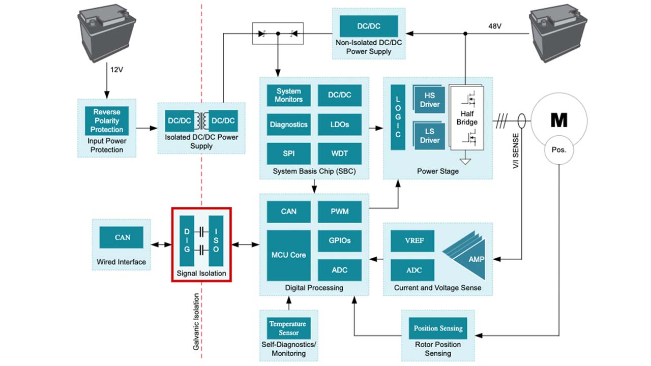
Figure 1 shows a starter generator system where the power stage, which includes the H-bridge and the field-effect transistors (FETs), is on the 48-V side. The switching of these FETs causes voltage transients (dv/dt) that may induce some common-mode noise on the 48-V ground. In the absence of any isolation, this noise will couple with the 12-V side and affect the signal integrity of circuits on the low-voltage side. By adding isolation between the two sides, as shown in Figure 1, you can improve common-mode transient immunity and signal integrity.


Figure 1: Starter/generator subsystem in a 48-V HEV


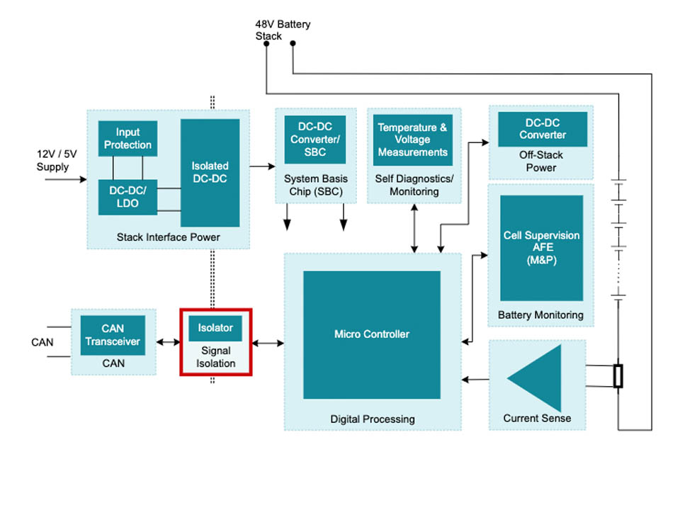
In Figure 2, a 48-V battery stack and microcontroller (MCU) in a battery management system (BMS) sits on the high-voltage side, while the MCU communicates with the electronic control unit using the Controller Area Network (CAN) protocol. If there is a fault on the 48-V side, the voltage could appear on the 12-V side. The circuit components on the low-voltage side (a CAN transceiver in this case) may not be able to withstand the high voltage and could become damaged. Having an isolator between the CAN transceiver on the low-voltage side and the microcontroller on the high-voltage side will ensure the safety of the low-voltage circuitry even if there is a fault on the high-voltage side.

The Verband der Automobilindustrie 320 (VDA320) standard for electric and electronic components in motor vehicles specifies a fault current test (E48-20) where the test voltage is applied across the 48-V/12-V barrier and the expected current between the 12-V and 48-V system must be less than 1 µA. The presence of an isolator ensures that the current will meet the standard.

Figure 2: 48-V BMS block diagram


If you are designing 48-V HEV systems and looking for isolation devices to interface with the 48-V side, there are a few options for communication between the 48-V side and 12-V side, depending on the interface standards.

For designs that require Serial Peripheral Interface (SPI), Universal Asynchronous Receiver Transmitter (UART) or general-purpose input/output (GPIO) communication between the 12-V and 48-V sides, you can use digital isolators such as the ISO7741-Q1 or ISO7721-Q1, depending on the number of channels of isolation you need.

When you are using I2C communication to save the number of signal traces, isolated I2C devices such as the ISO1540-Q1 (bidirectional data, bidirectional clock) or ISO1541-Q1 (bidirectional data, unidirectional clock) would serve the purpose.

If CAN communication exists between the two sides and isolation becomes necessary, you could add a digital isolator like the ISO7721-Q1 in series with the CAN transceiver or use an integrated isolated CAN device such as the ISO1042-Q1 to save some space.

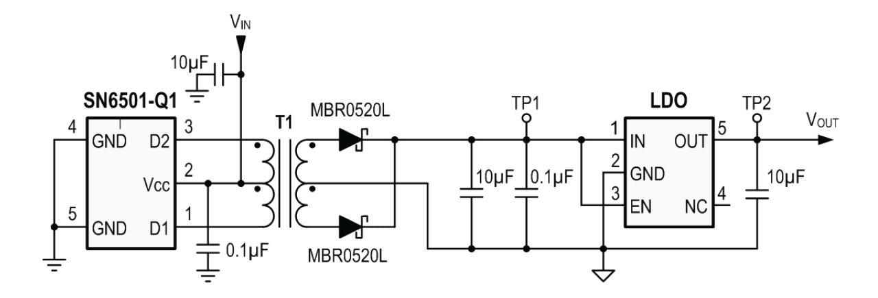
Data communication is just one part of the solution. You also have to isolate the power supply between the two sides, which you can achieve using flyback, fly-buck or push-pull topologies. For localized power supplies (for example, power for an isolated CAN transceiver), consider a transformer driver such as the SN6501-Q1, SN6505A-Q1 or SN6505B-Q1, that can be used with an external transformer, rectifier and low-dropout regulator, to generate a simple isolated power supply, as shown in Figure 3.


Figure 3: Simple circuit for an isolated power supply with a regulated output


The key differences between the SN6501-Q1, SN6505A-Q1 or SN6505B-Q1, is the output current of each driver, presence of spread spectrum to reduce emissions and different switching frequencies. These options enable you to select the right device to meet the emissions standards and power-supply requirements for your system.

While I’ve discussed these solutions within the context of 48-V HEVs, the isolation specifications of these device families and wider package options make these families suitable for EVs with higher battery voltages as well. It is possible to reuse the isolated sections from HEV subsystems in EV designs with minor modifications, which can save you both design and layout time.

Additional resources

How sensor-rich smart stores will make shopping a breeze

$
0
0


It's a Friday evening and you've decided to cook fish tacos. So you pop into your local supermarket on the way back from work. It takes several minutes just to hunt down the cilantro. Or, more accurately, to locate the empty shelf where the cilantro should have been. After another 10 minutes waiting in line for the single-staffed checkout lane, you finally get home to realize you forgot to buy tortillas. And that's how you end up spending your Friday night eating leftover casserole.

Data moves at almost the speed of light, but groceries don't. As the spread of high-speed internet renders information transmission ever-faster, the efficiency of the necessary physical transactions involved in buying and selling goods has lagged behind. That's about to change.


 Read our white paper, “Enabling modern retail and logistics automation.”
“A lot of companies both big and small are working on using sensor technology and machine learning to improve the shopping experience ,” said Gustavo Martinez, a system engineer at our company. “Customers are frustrated by things like standing in a long checkout line, or finding out that they don't have the item they want, or that it's more expensive than somewhere else.”
A personal shopper in your pocket

The combination of machine learning and GPS technology already allows retailers to deliver personalized advertisements as a potential customer enters their vicinity. The next step is the use of in-store sensors, such as Bluetooth beacons, to deliver hyperlocal promotions at the level of the individual shelf.

These might trigger a custom notification on a smartphone—such as a half-price offer on vanilla wafers to the customer who will spend several minutes staring at the cookie aisle. Alternatively, replacing paper price tags with LCD displays will enable flexible offers to be displayed on the shelf itself, changing as different customers are approaching.

These smart displays can also guide a customer around a store, Gustavo said. “The store's app can plot out the most efficient route to pick up all the items in your list, and we can have the in-shelf displays light up as you approach to make it easy to locate the item that you're looking for."

(Please visit the site to view this video)

The end of the line for the checkout lane

Among the most significant changes to the in-store experience has been the rise of self-checkouts. These aren't just about saving staffing costs for stores.

“The main thing is getting rid of the need to stand in line to check out,” Gustavo said. “At least in my case, having to wait that additional 10 or 15 minutes is my least favorite part of going to a store.”

Self-checkouts aren't perfect, however. There's still a relatively laborious process for entering uncoded items, such as loose fruit, and the need for a store assistant to dart between sale points to assist with problems and age-restricted items.

“Some companies are looking into integrating cameras into the self-checkouts that can use machine vision to identify the items you're buying,” said Aldwin Delcour, a systems engineer at our company. “Instead of having to search through a whole set of menus, you can just put your apple in front of a camera and the system can automatically identify it.”

While more numerous self-checkouts haven’t eliminated the line altogether, the end of the line may be coming. At stores on the cutting edge of retail automation, customers scan their phone as they walk in, and a combination of cameras and in-shelf sensors tallies up the items put into their basket and automatically bills them when they leave.

Currently, this requires sending streams of data from potentially hundreds of thousands of stores up to the cloud for processing by machine learning algorithms.

“That's an enormous amount of data being siphoned off, which can present significant challenges,” Gustavo said. “So we're looking at how that data can be processed in the store itself to reduce that load.”

Gustavo Martinez and Aldwin DelcourGustavo Martinez (left) and Aldwin Delcour (right) 

TI mmWave sensors, which bounce high-frequency radio waves off an object to precisely identify its shape, size and distance, can simplify the recognition task, potentially allowing it to be performed in-store on our Sitara™ processors, specifically designed for low-power machine learning applications.

The highly-sensing store that's never out of stock

Smoothing a customer's journey through a store also includes making sure items they want are where they should be. Ubiquitous sensing will not only enable stores to track customers but also stock, ensuring that low-levels of an item can be detected instantly and supply ordered.

"A store might have a spring mechanism so that when you take an item, a new one is pushed forward," Aldwin said. “You can put a sensor in the back that detects how far it has moved, and then gives a signal to a centralized computer that the inventory is low and it might be time to order the next shipment.”

Once the inventory order is placed, the same technology that guides customers around a store can also be used to guide stock pickers around a warehouse, making the process of filling an order much faster and more efficient.

A Future Friday evening

The future of grocery shopping could look like this: It's a Friday evening, and the app for your local supermarket sends you a recipe for fish tacos. Based on your previous shopping behavior, the company's machine learning algorithms have built up a profile of you as a Mexican-food lover who enjoys Friday night cooking, and the recommendation is perfect. You click to add the ingredients to a digital shopping list and head to the store.

As you walk through the door, a notification pops up offering a map of where all your ingredients are located. The label beneath the relevant item lights up as you approach and nothing is out of stock.

Once all the items are in your basket, you walk straight out the door. No security guard chases after you. Instead, your phone delivers a receipt and informs you that all of the items have been charged to your account.

The whole process took a few minutes, and you arrive home early with a full set of fish taco ingredients. The rest is up to you.

How to flexibly configure an LED driver for automotive headlights

$
0
0

Electronic technology has advanced so that an electronic control unit (ECU) is required to control the functions of full LED automotive headlights. An ECU consists of mainly LED drivers for headlight functions such as high beams, low beams, daytime running lights, position lights, turn indicators and fog lights. In this article, I’ll explain the advantage of having a flexibly configurable LED driver.

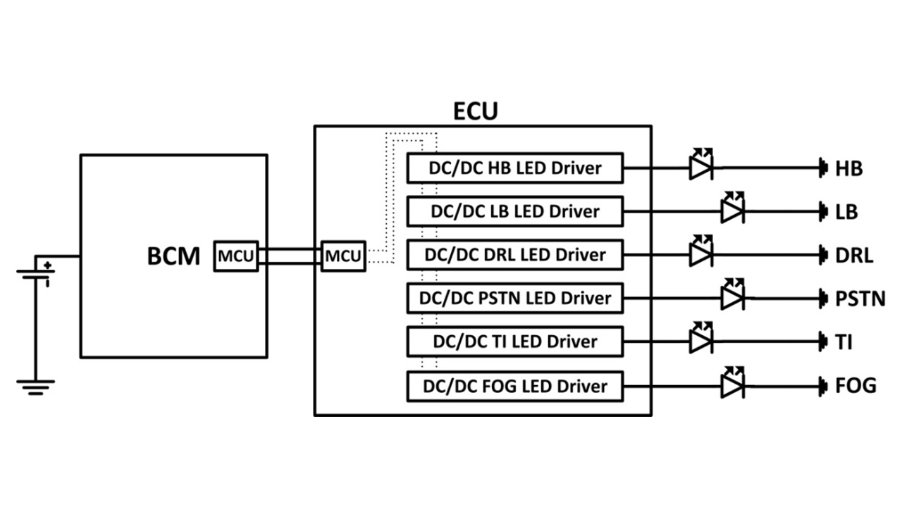
When LEDs were first introduced into the automotive headlight space, high-side switches connected to LED drivers drove the corresponding LEDs in each of the headlight functions. Figure 1 shows a block diagram of a traditional automotive body control module (BCM) with LED drivers for corresponding headlight functions. The LED and input voltage relationship per headlight function determine the best DC/DC topology.

Figure 1: Traditional automotive BCM with DC/DC LED drivers for LED headlights

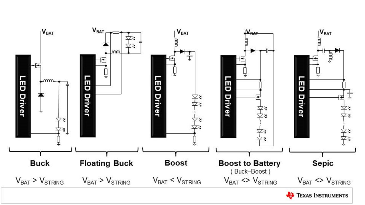
Figure 2 shows basic schematics of common DC/DC LED driver topologies and their voltage relationships.

Figure 2: Basic schematics of common DC/DC LED driver topologies

Except buck LED drivers, which require a high-side metal-oxide semiconductor field-effect transistor (MOSFET), all other topologies can be implemented with a low-side MOSFET controller. Hence, a low-side MOSFET controller is one of the necessary elements to build a flexibly configurable LED driver.

As electronic technology advances and car manufacturers feel more comfortable adding electronic controls to their vehicles, a modern full LED automotive headlight will employ an ECU with a modernized BCM, including microcontrollers (MCUs). The ECU should be able to communicate through the MCU upon receiving commands from the BCM and all headlight functions are controlled accordingly. Figure 3 shows a modern architecture for a full LED automotive headlight.

 Figure 3: Modern architecture for full LED automotive headlight

The MCU in the ECU receives information from the BCM to determine which headlight function to turn on or off. More advanced models might require the ECU to change individual headlight brightness based on BCM commands. It would be best to have an effective digital protocol control, such as SPI, within the ECU such that the MCU can communicate with individual DC/DC LED drivers through the digital interface.

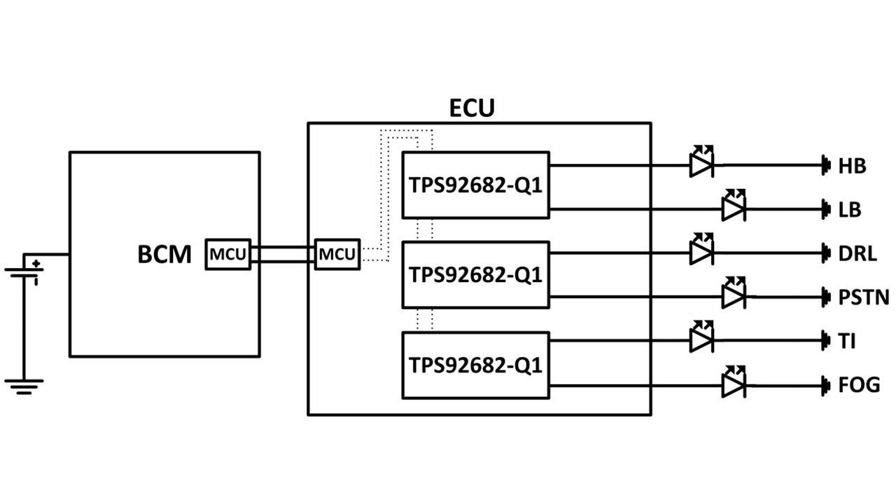
The TPS92682-Q1 is a dual-channel low-side N-type MOSFET controller with Serial Peripheral Interface (SPI) for parametric setup through digital controls. With a low-side N-type MOSFET controller, different DC/DC LED driver topologies can be built, such as boost, boost-to-battery, single-ended primary inductor converter and floating buck. SPI enables the MCU to provide parametric setup information through digital protocols. More importantly, the dual-channel device has two fully independent controllers that can be programmed flexibly according to the ECU’s commands.  As illustrated in Figure 4, it’s possible to build a six-channel ECU with three TPS92682-Q1 devices.

 Figure 4: Six-channel ECU example block diagram with the TPS92682-Q1

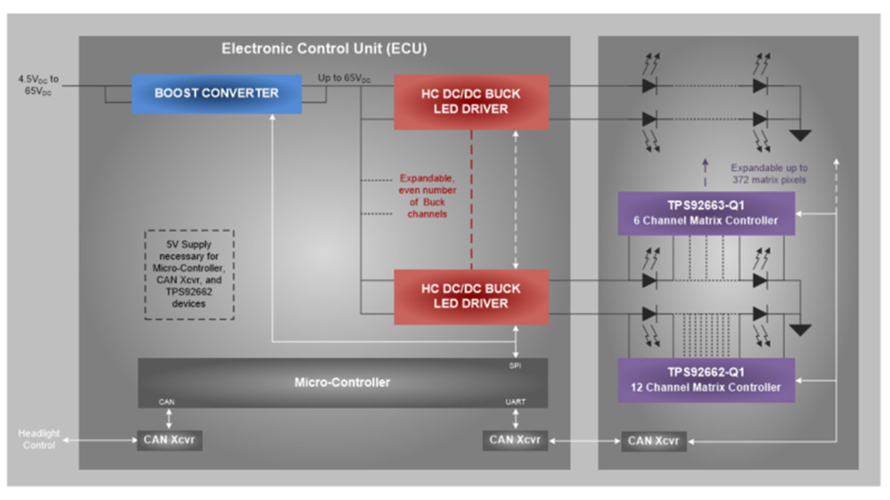
The TPS92682-Q1 has the ability to configure channels to be current output or voltage output. Simple ECUs normally provide current sources to LEDs for different headlight functions. More advanced headlights, such as matrix LED headlights, require that the LED drivers be in a boost-to-buck configuration for pixel brightness control compatibility with LED matrix managers. Figure 5 shows a typical ECU block diagram for an advanced headlight.

Figure 5: Typical ECU block diagram for an advanced headlight

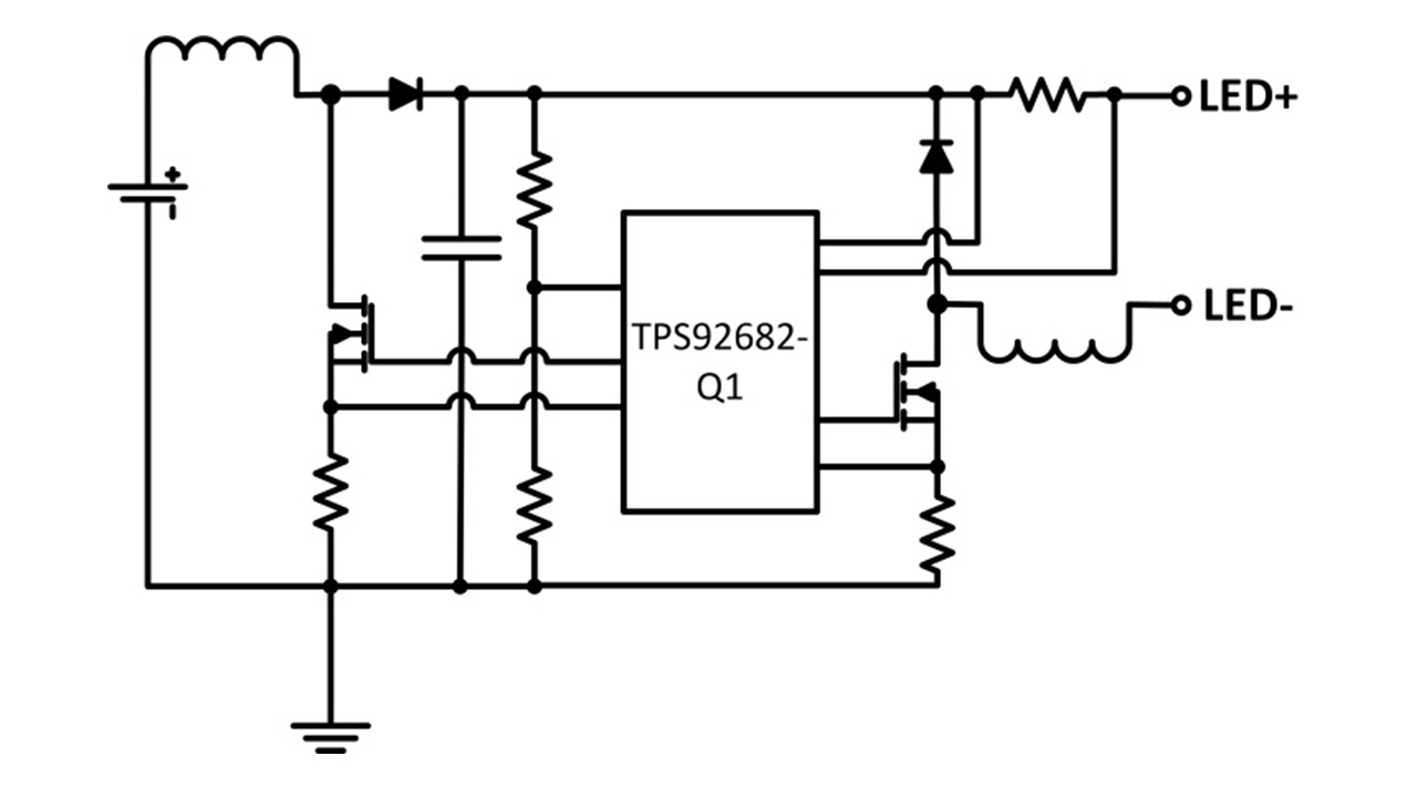
The two channels of the TPS92682-Q1 can be programmed to run as a two-phase voltage-output regulator. This enables high output power – up to 120 W. However, there are simple headlight LED drivers that require a boost-to-floating-buck architecture. By configuring one channel as a boost voltage output with another channel configured as a floating buck current output, it’s possible to configure a simple boost-to-floating-buck LED driver with a single TPS92682-Q1 device. Figure 6 shows a concept schematic of a boost-to-floating buck using the TPS92682-Q1.

Figure 6: Concept schematic of a boost-to-floating buck using the TPS92682-Q1

As automotive headlights move from bulbs, xenon and high-intensity lamps to LEDs, the TPS92682-Q1 helps implement a flexibly configurable automotive headlight ECU that can communicate with a modern BCM.

Additional resource

Fast and furious: designing longer-lasting 16S-17S Li-ion battery packs for e-motorcycles

$
0
0
With the rapid growth in demand for delivery services, electric motorcycles (e-motorcycles) are becoming more popular as a transportation method because the battery capacity is much larger than e-bike/e-scooter batteries. More capacity enables longer...(read more)

Engineering hope for rare diseases

$
0
0

Gina and Joseph HannGina and Joseph Hann

Gina Hann walked into her son’s kindergarten class wearing zebra stripes and armed with enough black-and-white snack cakes to build a small fort.

It was national Rare Disease Day, and Gina, an engineer at our company, was on a mission to talk to 6-year-olds about rare diseases. She explained why a zebra – a term in medicine that indicates an unlikely diagnostic possibility – is the perfect mascot for children like her son, Joseph, who was diagnosed with a terminal and degenerative brain disease in 2017.

Gina and Joseph Hann“When you ask small children what makes a rare-disease child different from them, they give you beautifully candid answers,” Gina said in a blog post. “Things like: ‘He has a wheelchair. He drools. His words sound different. His eyes don’t work.’ Those statements hold no judgment, just honesty.”

As the mother of that rare child, Gina took the opportunity to turn her son’s challenges into a celebration of differences.

“When you ask small children what makes a rare-disease child the same as them, they celebrate the discovery,” she said. “He loves music, and instantly they sing with him. He loves laughter, and they all laugh with him from their bellies. I think kindergartners should rule the world.”

For Gina, good days like these make the difficult fight worth it. Since learning about her son’s disease, Batten, she has been on a nonstop journey to bring hope to other families dealing with a similar diagnosis and to make gene therapy for rare diseases more accessible. Initially, she and her husband, Matt, were told to make end-of-life plans for Joseph since no clinical trial or funded research existed to find a treatment.

“We didn’t know it then, but Joseph’s story was just beginning,” she said.


 Hand and heartLearn more about how Gina and Matt helped bring hope to their son and countless others.

‘A relentless process’

Gina and Matt were told that if they wanted a clinical trial for their son, they would need to fund the work themselves, and that would mean raising a million dollars or more just to cover the first steps before a clinical trial could be developed.

Ever the engineers and problem-solvers, Gina and Matt searched for a solution. They founded Joseph’s Foundation for Batten Hope, a nonprofit organization dedicated to raising funds toward a clinical trial for a potential cure and gene therapy work at The Children’s Medical Center of Dallas and University of Texas Southwestern Medical Center.

“Matt and I challenge ourselves to innovate and work for better outcomes by the nature of our jobs and our work environment at TI,” Gina said. “We knew to ask if there could be more out there, to question everything and to always look for what’s next. That’s why we felt compelled to choose the path we did – it was a relentless process, but our work helped to make us uniquely suited for it.”

Gina and Matt have helped raise more than $1.5 million and have located over 20 other families around the world who are in need of treatment for their loved ones. Today, they’re working toward funding the final materials needed for the trial, which they hope will begin in early 2020.

“We don’t know if we’ll have the treatment in time to save Joseph’s life,” Gina said. “But no matter what, Joseph has inspired the work that can save the lives of countless others.”

Commitment to the rare disease community

Gina’s commitment to fighting rare diseases is expanding even further: She has joined efforts with other rare-disease family foundations in the Dallas area to establish a new nonprofit called RARE Dallas, which is focused on connecting and empowering affected families and finding cures. As a result of her outstanding commitment to the community, she was recently recognized with our company’s TI Founders Community Impact Award, which honors our company’s founders and their long history of philanthropy and volunteerism in communities where we live and work.

“I think for a lot of parents, when the doctor tells them to make end-of-life plans for their child with a rare disease, they are so overwhelmed that they don’t stop and to challenge if there could be other options,” Gina said. “We want to make it well known that just because a treatment hasn’t been developed yet, that doesn’t mean it can’t be done.”

Gina and her family are living proof that you can engineer your own hope.


“There is so much beautiful hope in this world,” Gina said. “Especially knowing that one day soon, the kindergartners will run the place.”

To stay updated on Joseph’s story, follow Batten Hope on Facebook and Instagram.


How to boost the performance of your resolver – without compromise

$
0
0

Motor control is an essential part of electric vehicles, which generally use permanent magnet AC motor (PMAC) or induction motors. There are advantages to both types, as well as trade-offs.

PMAC motors can use resolvers or encoders. A resolver converts mechanical motion into electrical information pertaining to the absolute rotary position. It consists of a primary winding and two secondary windings. The secondary windings are on a stator at a 90-degree angle relative to each other, whereas the primary winding is on the rotor. Other types, such as variable reluctance, have all three windings on the stator.

When an excitation current is applied at the primary winding, the sine/cosine secondary windings will output the same frequency signal while being 90 degrees out of phase. You can use the magnitudes of the two secondary windings to calculate the exact position of the shaft relative to the stator.

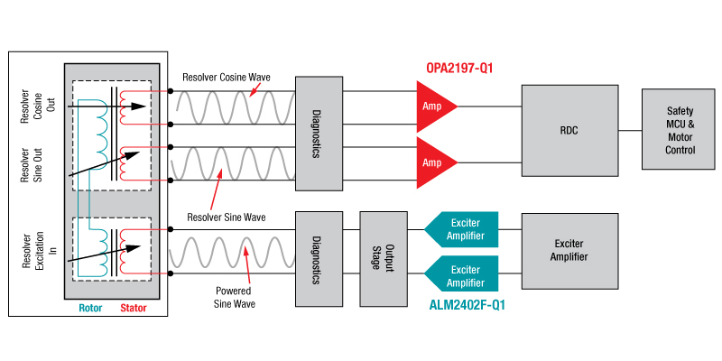
Figure 1 shows an example of a resolver-based circuit with the ALM2402F-Q1.

ParametersDescriptionTypical range
Input voltageInput voltage to the resolver primary coil R1/R23 VRMS-7 VRMS
Input frequencyExcitation signal frequency applied to the resolver primary coil R1/R21 kHz-20 kHz
Transformation ratioRatio between the resolver’s primary and secondary coils0.2 V/V-1.0 V/V
Input impedanceInput impedance of the resolver (resistance-inductance)30 Ω, 80 mH
Phase shiftPhase shift between the resolver excitation signals and sine/cosine signals from the secondary coil±25 degrees
Pole pairsNumber of sine/cosine output cycles per mechanical rotation1-3
Supply voltageSupply voltage provided to the analog front end12 V-26 V
AccuracyOutput angle readout accuracy≤0.1-degree error
Resolution16 bits
TemperatureSystem temperature-40°C to 125°C
AmplitudeDesirable sine/cosine amplitude3.3 Vp-p
Frequency 
AttenuationResolver voltage attenuation 0.4 Vp-p0.4Vp-p

Table 1: Typical parameters for resolver-based measurements

One of the critical tasks in choosing the right device to drive the primary coil is to assure the minimum slew rate for the excitation amplifiers so that you can avoid slew-induced distortion. Equation 1 calculates the excitation voltage as the ratio of the sine/cosine amplitude over the attenuation:

(3.3/0.4) = 8.25 Vp-p    (1)

Equation 2 expresses the minimum slew rate to avoid distortion:

SR = 2*π*Vp*f = [(2*6.28*(8.25/2)*20000)]/1E6    (2)

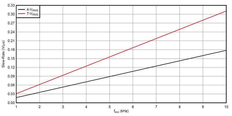
Equation 2 yields 0.52 V/μs.

Figure 2 shows the minimum slew rate required for the excitation amplifier.

Figure 2: Minimum slew rate needed for an excitation amplifier vs. frequency

 Resolver-based measurement methods

There are two common methods for resolvers: a software-based resolver-to-digital converter (RDC) with a microcontroller (MCU) and an integrated circuit RDC. The MCU generates a pulse-width modulation (PWM) signal that is modulated into a sine wave. Active low-pass filters then filter out the PWM carrier frequency and rid the system of undesirable harmonics, leaving only the excitation frequency component for the primary circuit. Active high-pass filters remove DC offsets.

Once the signal is filtered out, it needs conditioning using high-output current amplifiers, which is again achievable with a discrete solution using low-noise op amps such as the OPA2197, along with BJT transistors or integrated dual power amplifiers like the ALM2402F dual op amp. The ALM2402F offers not only a high output current (400 mA) but also thermal shutdown and a current limit, along with an integrated overtemperature fault flag.

The other area of interest is the aforementioned analog front-end portion of the circuit, which comprises three difference amplifiers. The first amplifier monitors the output of the excitation amplifier to detect phase lags caused by low-pass filters (through the MCU), or faulty conditions, which may have been caused by the excitation amplifier. The other two amplifiers are used to buffer the sine and cosine signals coming from the secondary windings of the resolver. An example of this is shown in Figure 3, which represents a typical analog front end for a resolver-based application.

Figure 3: Typical resolver front end

The key to designing a good difference amplifier is the matching of the external resistors used for gain control. While discrete op amps such as the OPA2197-Q1 provide very good DC performance (low input offset voltage and drift), common-mode rejection will depend on resistor matching. A pair of 0.005% matched resistors achieves 86 dB.

Safety (ASIL) requirements

Another important aspect to designing a resolver circuit is the need to abide by functional safety standards. Although there are several standards across many sectors, automotive hardware engineers must adhere to International Organization for Standardization 26262 safety requirements to support Automotive Safety Integrity Level (ASIL) A to ASIL D. ASIL is a critical part of the design in applications like electric power steering, transmission gear boxes, braking systems and advanced driver assistance systems. The point of complying with functional safety standards is to mitigate risk in case of a malfunction. If failure occurs in a motor-control system, the functional safety part of the circuit can detect a faulty condition and respond accordingly to remedy the problem. One way to implement a safety circuit is to use two components for redundancy in the excitation part of the circuit within the resolver. One integrated such as the ALM2402F-Q1, the other in a discrete fashion like the OPA2197-Q1.

Resolvers have become more popular in recent years because they can operate in harsh environments, withstand high temperatures and provide accurate measurements. Selecting electronic components requires extra care, however, since they are usually located a distance away from the resolver itself, which makes noise immunity and common-mode rejection ratio paramount to achieve the desirable performance.

Texas Instruments precision amplifiers (including the ALM2402F-Q1 and OPA2197-Q1) have integrated electromagnetic interference (EMI) filters within the input stage to minimize the effects of undesirable radio-frequency injection. To learn more, visit the resources below.


Additional resources:

Maximizing machine-learning inference at the edge

$
0
0

Employing machine learning and neural networks in factories improves applications like machine vision, automated guided vehicles (AGVs) and robotics by making them smarter, which improves operational efficiency. Embedded microcontrollers and processors have been used for decades in manufacturing to automate repetitive processes, but deploying machine-learning algorithms to embedded systems beyond research prototypes is still in its infancy.

Let’s take a look at one application of machine learning in a factory. Today, AGVs receive input from sensors such as cameras or radar. Software running on a processor analyzes the data and makes decisions that control the electric motors and move the AGV around the factory safely. In a constrained environment like a warehouse, classical machine-vision algorithms can be successful, but machine learning can outperform them because can adapt to slight changes in such environments and enable more human-like perception and classification, which is critical as factories evolve to meet three key needs:

  • Reduced navigation space as warehouse density increases.
  • The ability to classify objects on the factory floor, not just detect them.
  • The coexistence of AGVs in a shared space with humans.

 How machine learning enables Industry 4.0

Machine learning inference is a powerful tool for processing and understanding information, specifically in machine vision, where it has been shown to outperform not only classical algorithms, but also humans in terms of accuracy. Such capabilities are achieved through deep learning, which is a subset of machine learning that uses deep neural networks trained with a large amount of data.

To deploy machine- or deep-learning algorithms in an embedded system, the first step is to collect a data set of what requires classification or detection; for example, millions of images of obstacles that may exist on a factory floor, such as a person, a static machine, a robotic arm, shelving or boxes. You would then import this data set into an offline training program that learns to look for patterns or anomalies in the data. This step is not performed in real time, but is a computationally intense process that runs on servers or in the cloud. For machine vision, the output of this process is a trained network model that can be deployed on a processor at the edge of the network. For an AGV, machine-learning inference significantly improves the analysis of what its cameras see, which can then be used to take action, such as to avoid a box in its path.

Deploying machine learning in an industrial embedded system

The inference capabilities of a machine-learning-enabled processor apply the knowledge of a trained network to a given image or frame in a sequence of images. TI Sitara™ processors are embedded inference processors that enable equipment manufacturers to deploy machine-learning algorithms and automate applications like machine vision for AGVs.

Figure 1 illustrates a machine-learning example I ran on the TI AM5729 processor to show a semantic segmentation of pixels that identify three classes common in a factory: the AGV’s path (green), another vehicle (blue) and people (red).

Machine learning inference with Sitara processors

Figure 1: An example to illustrate the role of labeled data and machine learning

To illustrate how an AGV might operate, we used the jsegnet21v2 network from TI’s processor software development kit (SDK) on an image applicable to AGVs in a warehouse setting. The example is trained on the cityscapes data set; for a production AGV, you would need to collect and label the pictures applicable to your environment to train the selected network.

Using the TI deep learning (TIDL) software framework, I deployed our algorithm on the Sitara AM5729 processor. The AM5729 processor ran the algorithm on a 1,024-by-512 pixel frame at about a dozen frames per second using the four embedded vision engine (EVE) cores on the device, and consumed less than 0.5 W of additional power. Each of the four EVE cores is a coprocessor able to perform 512-bit-wide vector multiply-accumulate operations that dominate the computational needs of neural networks. In real-time cyberphysical systems like AGVs, latency matters as well as throughput (frames per second). The frame processing latency on the AM5729 is approximately 250 ms (four frames in parallel), very likely sufficient to make decisions regarding the velocity of an AGV in a warehouse.

Reducing latency in machine-learning inference

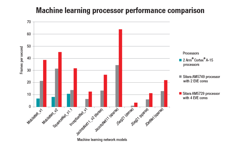
In a typical example classification application using a network model like MobileNetv2, the high frame rate with low batch size achievable with the AM5729 translates to a 30%-40% decrease in inference latency per frame compared to the AM5749, which has two EVE cores. MobileNetv2 classification on 224-by-224-pixel images can run at 45 frames per second on the AM5729 processor. With less than 2 percentage point accuracy compromise, sparsification and TI’s EVE-optimized deep-learning network model JacintoNet11, it is possible to improve the inference latency even further.

You can acquire or collect data and train your algorithms using these popular frameworks, and deploy your algorithms on Sitara AM5729 processors using the TIDL interface. Testing shows that processors with EVE cores underneath the inference run faster than on processors with just ARM cores. Figure 2 compares the frames-per-second performance of two Arm® Cortex® A-15 processors against the AM5729 and AM5749 processors on some popular deep-learning networks. The Cortex A-15 performance is measured using Arm’s NN 19.05 software, while the EVE performance uses the TIDL software framework in Processor SDK version 6.1.

Machine learning processor comparison chart

Figure 2: Frames-per-second performance of processors across various machine-learning networks

Today’s distributed factories and breadth of applications will require machine-learning inference algorithms built on popular platforms like Sagemaker NEO and TensorFlow Lite that can run using the various network models listed in Figure 2. The ability to support these popular platforms is critical to manage the use of machine-learning inference everywhere as factory automation evolves.

Conclusion

Industrial embedded applications are about solving real-time use cases in the physical world,  that can be proven with digital micro-benchmarks like frames-per-second throughput. In practice, the performance of the Sitara AM5729 processor enables the processing of typical camera inputs in real time, with frame rate, latency and power consumption relevant to multiple factory applications. To evaluate machine-learning functions with the AM5729 processor, the BeagleBone AI evaluation board offers a low-cost option for getting started.

Additional resources


Selecting TVS diodes in hot-swap and ORing applications

$
0
0

Designers will often use a transient voltage suppression (TVS) diode to clamp large surge currents to a safe voltage level in order to protect nearby components from damage. In many ways, a TVS diode behaves like a Zener diode, but with a higher power-rating capability because of its larger die size and stronger wire bonding.

Why do hot-swap applications need a TVS diode?

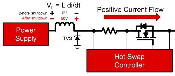
In a hot-swap application, if there is a large overcurrent fault, then the protection integrated circuit (IC) will shut off the current quickly in order to shield nearby components from damage. This fast shutdown of current – from maybe 50 A (overcurrent) to 0 A (shutoff for protection) – can occur within tens of nanoseconds and results in a large current transient (di/dt), as shown in Equation 1:

This current will be trapped as energy inside of trace or wire inductance on the input. Although the trace inductance may be low, at a value of about 10 nH, it will still produce a surge on the input of the hot-swap controller, based on Equation 2:

That -50-V surge will be in series with the input power supply and will effectively create a positive voltage spike on the input rail, often exceeding the voltage rating of the hot-swap controller IC or metal-oxide semiconductor field-effect transistor (MOSFET) drain-to-source voltage (VDS) (see Figure 1). To prevent this voltage surge from occurring, you can place a TVS on the input to divert energy from the inductance straight to ground. The optimal placement of the TVS will be after any series inductance on the input (such as after a fuse).

Figure 1: Inductive kickback after hot-swap controller shutdown. The voltage across the inductor, VL was previously 0 V during normal operation; after fast current shutdown, VL equals 50 V and will be added in series to the input power supply

How do you choose a TVS diode?

The simplest way to pick a TVS diode for a hot-swap application is to choose one that meets the following three criteria:

  • A voltage breakdown, VBR, greater than your maximum power-supply input voltage.
  • A clamping voltage, VC, below the absolute maximum rating of your hot-swap controller IC or MOSFET VDS.
  • A peak pulse current rating, IPP, above the peak current at which the hot-swap controller will shut off. This worst-case value is often the current visible if there is a short circuit on the output and the hot-swap controller shuts off. An accurate value to use would be the peak current measurement on an actual prototype board, with a realistic short circuit applied to the output.

For a 12-V high-power application, a common TVS choice is the 5.0SMDJ12A, which has a 5-kW transient power capability. For a deeper analysis of the equations used in choosing a TVS diode for a hot-swap application, check out the Power Electronics article, “TVS Clamping in Hot-Swap Circuits.”

How to design more noise-tolerant industrial systems

$
0
0

Modern factories and other industrial settings consist of a rich mesh of interconnected machines that themselves include devices such as networked computers, programmable logic controllers, input/output cards, field transmitters, sensors, and a collection of wired and wireless communications networks. The amount of data generated and communicated within factory environments has increased dramatically in the last few years, as companies race to monetize the efficiencies and agility that smart factories bring.

However, connecting factory equipment has unique challenges. One of these challenges is the vast array of electrical noise generated by factory equipment such as motors, switching power supplies, high-voltage distribution cables and other similar sources. A variety of system impairments such as bit errors, signal degradation, signal amplification, signal loss or a combination of these will generate electrical noise, ultimately resulting in system malfunctions that range from unnoticeable bit glitches to catastrophic system failures that could endanger lives or result in the processing of unusable goods.

Industrial system designers must pay special attention to the impact that noise from a factory environment can have on the robustness of their design and create layers of noise protection; for example, implementing system circuit designs that are noise-tolerant in case noise makes its way into a system’s circuits.

Multiple design techniques exist to mitigate and overcome this type of electrical noise; all engineers should use building-block devices like logic circuits, which have a higher level of noise immunity. Logic circuits play a critical role in bringing a system’s circuit components together, and as such act as gateways for control and data signals of a system’s circuit implementations. Using logic devices with higher noise immunity basically means stopping noise at these gateways before it can propagate through a system.

One critical feature of logic devices that helps improve noise immunity is Schmitt-trigger inputs. Standard complementary metal-oxide semiconductor (CMOS) inputs are susceptible to noise: noisy inputs can cross the input threshold multiple times, causing oscillations at the output (as illustrated in Figure 1), potentially resulting in system errors. In contrast, a Schmitt-trigger input design separates the positive and negative-going thresholds.

 Figure 1: Standard CMOS inputs vs. Schmitt-trigger inputs

Logic circuits with Schmitt-trigger inputs have outputs that will switch only once; they will also have clean signal edges for any CMOS input (see this Schmitt-trigger video, “Eliminate slow or noisy input signals,” for a detailed explanation). Given the importance of using logic building-block devices with Schmitt-trigger inputs for noisy industrial applications, logic device selection becomes an important step.

TI’s HCS logic family makes the logic selection process easy for industrial applications by providing a portfolio where every logic device includes Schmitt-trigger inputs. Encompassing all major logic function types, the HCS family enables industrial system designers to confidently implement noise-tolerant and robust system control and data logic interfaces.

Additional resources

How tiny data converters give you more value per square

$
0
0

(Note: Kaustubh Gadgil and Robert Schreiber co-authored this technical article.)

With the increased trend toward smaller systems, every square millimeter of printed circuit board (PCB) area matters. At the same time, with the increased demand for data, more sensors need to be monitored.

In this article, we’ll discuss how you can significantly reduce PCB footprint, increase channel density, and leverage higher integration of other components and features with TI’s small data converters, providing more value in a smaller size.

Benefit No. 1: a smaller PCB footprint

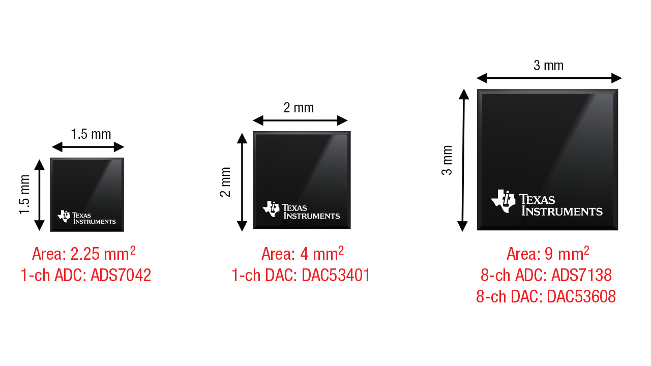
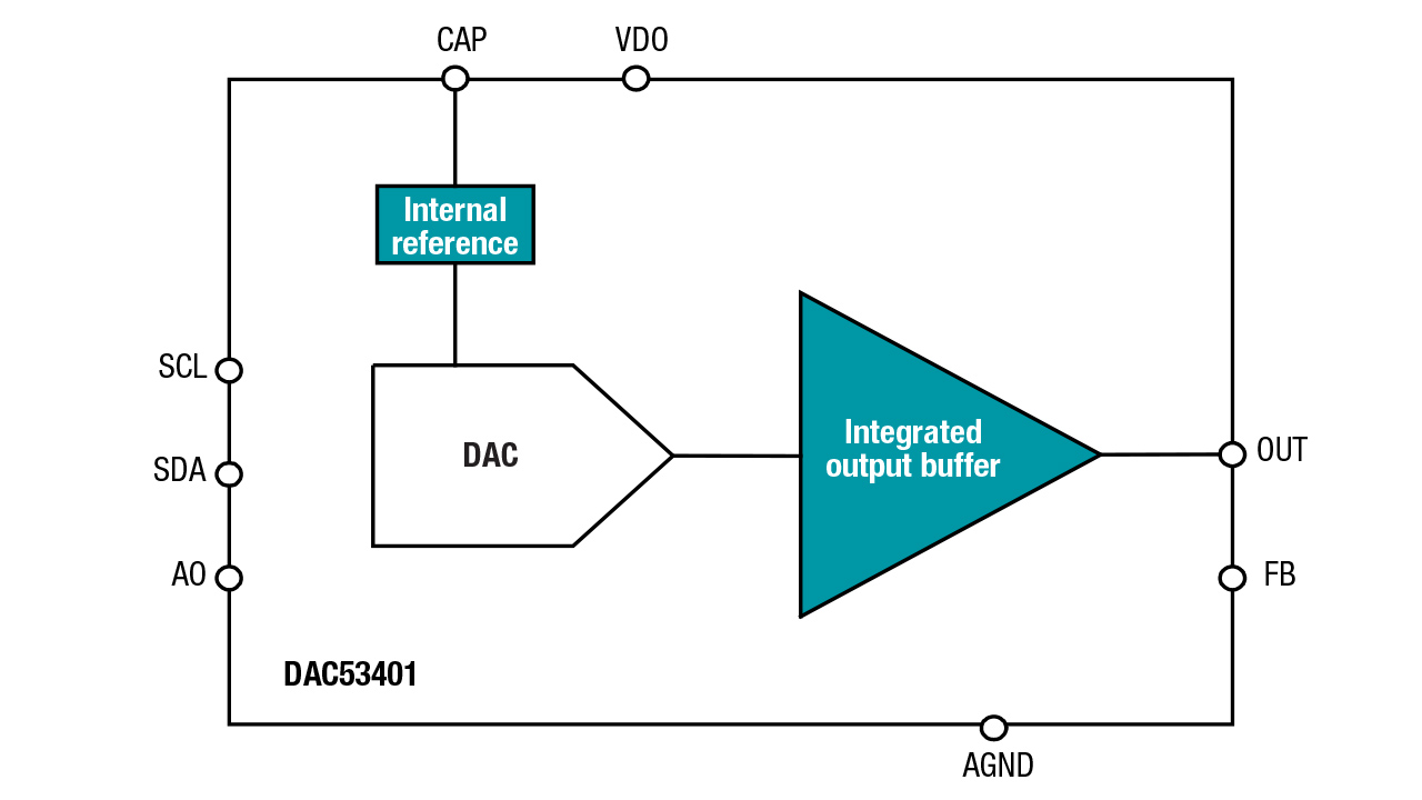
With advancement in design and packaging technologies, electronic components have gotten smaller. As shown in Figure 1, TI’s latest single-channel ADC, ADS7042, is available in a 2.25-mm2 footprint, nearly half the size of comparable ADCs of a decade ago. Similarly, TI’s latest single-channel DAC, DAC53401, is one-fourth the size of comparable DACs of a decade ago. Likewise, for multi-channel applications, TI’s latest 8-channel ADC (ADS7138) and DAC (DAC53608), are both offered in a footprint of 9 mm2 (~1 mm2 per channel).

Figure 1: TI’s smallest data converters

These tiny data converters allow you to reduce the PCB size for space-constrained designs or pack more channels into the same PCB size, or both.

Benefit No. 2: integration of analog functions

Many systems use discrete components and passives to implement a variety of analog functions, such as signal conditioning, biasing and comparators. Because TI’s smaller data converters integrate these functions, they eliminate many discrete and passive components, thereby reducing PCB size, simplifying design, improving performance and increasing reliability.

Some examples of such integration include:

  • Fewer external components
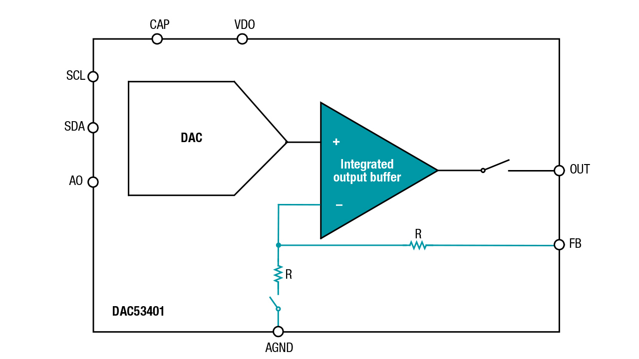
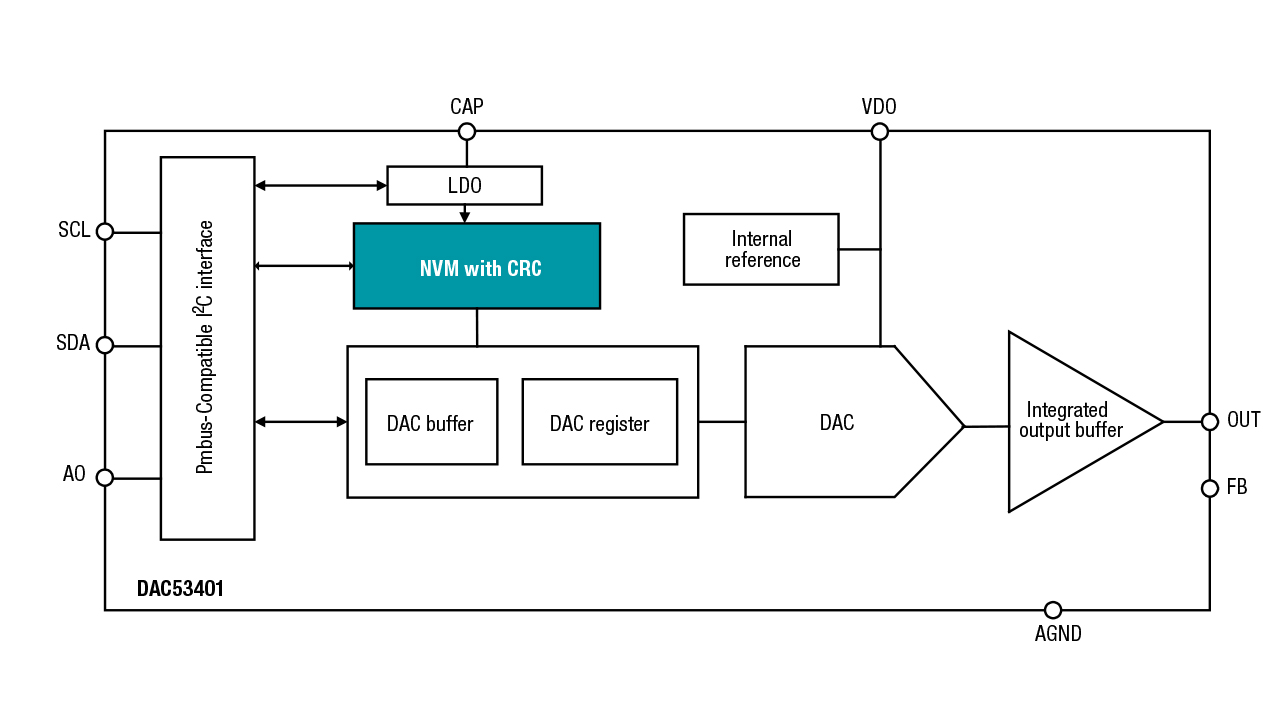
    As shown in Figure 2, DAC53401 integrates an output buffer as well as an internal reference, saving PCB area and cost.

Figure 2: Integrated reference and buffer in DAC53401

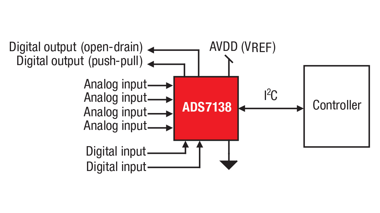
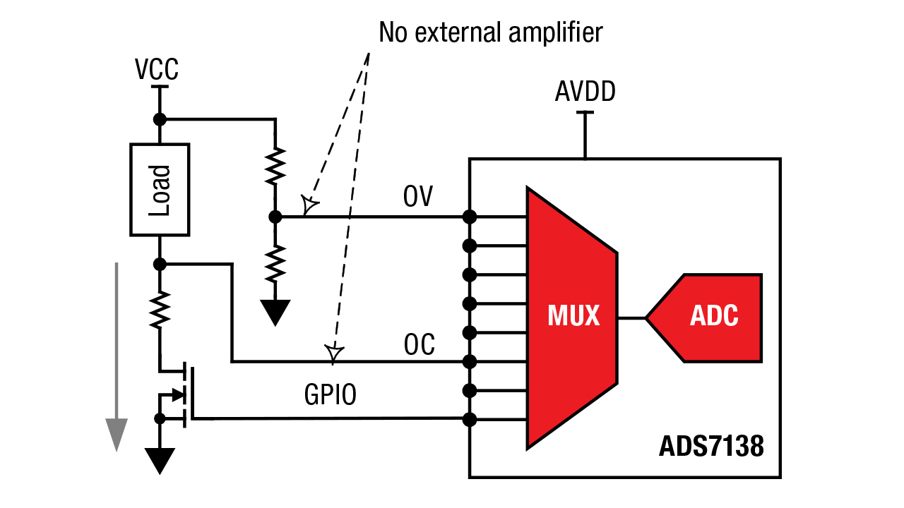
Another example is the ADS7138 shown in Figure 3, which does not need a driver amplifier at the input for most applications, again saving PCB area and cost.

Figure 3: ADS7138 eliminates the need for an external amplifier

  • Bias voltage generation, both fixed and variable
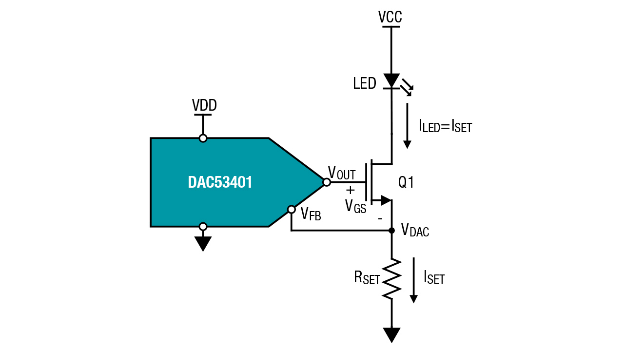
    The electrically erasable programmable read-only memory (EEPROM) and slew-rate control features of the DAC53401 are a good fit for generating fixed or variable bias voltages. Figure 4 shows an example of a lighting application.

Figure 4: DAC53401 biasing an LED

  • Analog and digital comparator
    Comparators are often used in systems to alert the host controller immediately if any of the critical signals, such as currents, voltages and temperatures, deviate outside their expected range. This comparator should have fast response time and avoid false alarms.

    As shown in Figure 5, the separate feedback pin (FB) enables you to use the DAC53401 as an analog comparator with a programmable threshold voltage.

Figure 5: DAC53401 offers access to the feedback path of its internal amplifier

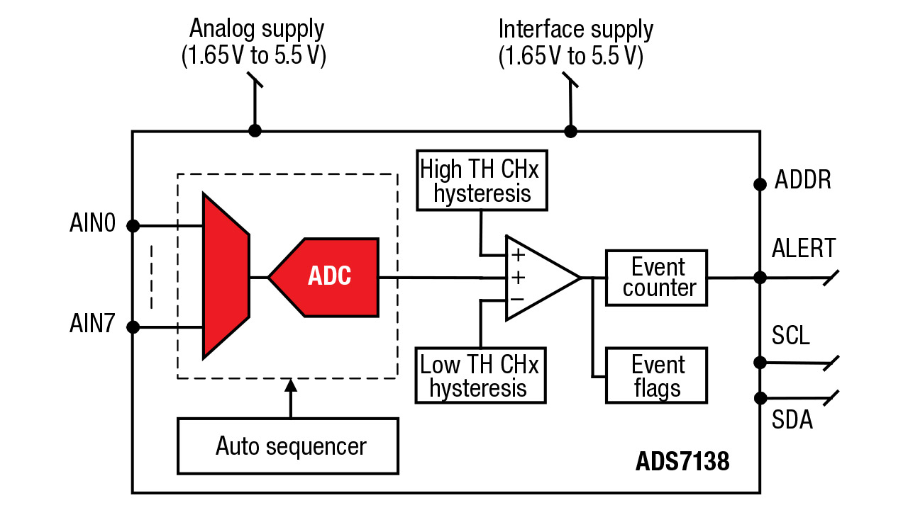
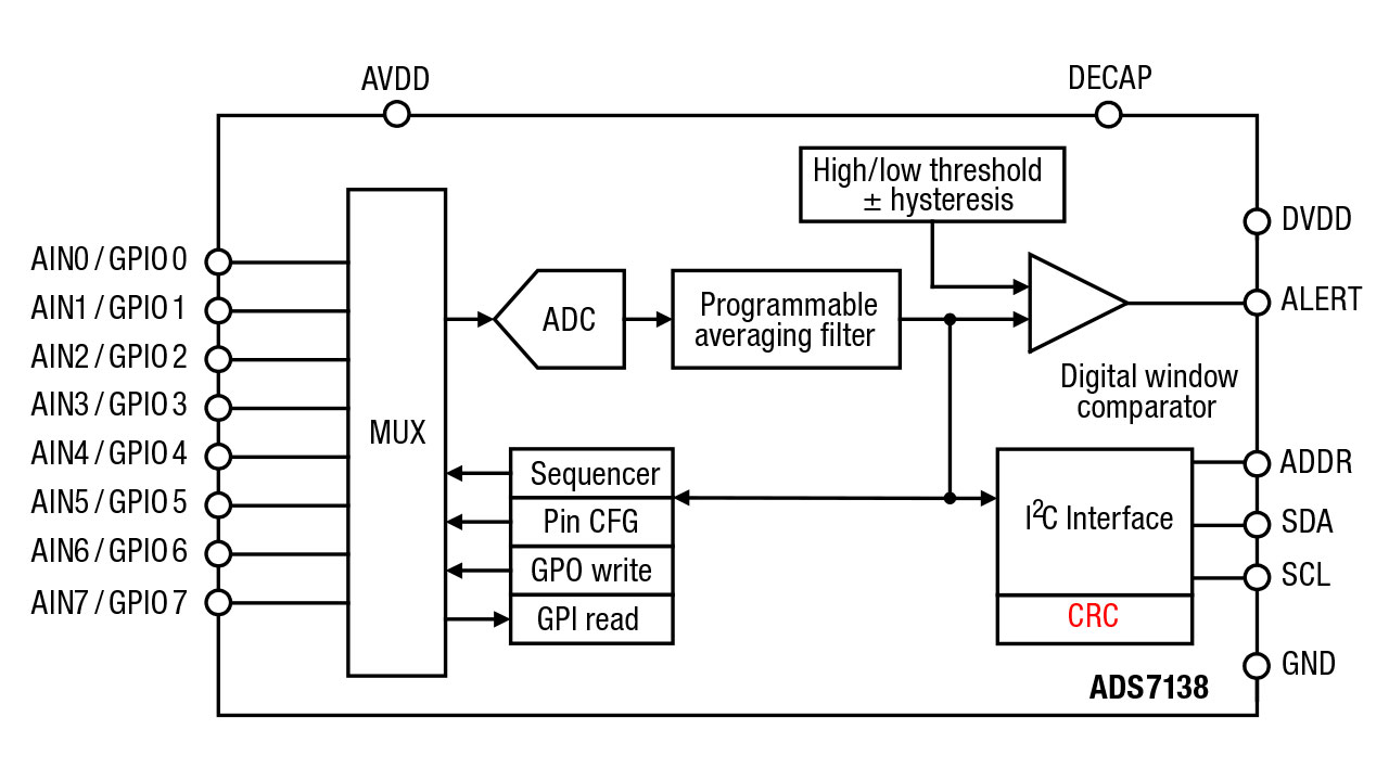
As shown in Figure 6, the ADS7138 integrates a digital comparator function with features such as programmable thresholds, hysteresis and event counter, which significantly reduce the possibility of getting a false alarm.

Figure 6: ADS7138 as a digital comparator

Benefit No. 3: integration of digital features

A smaller data converter not only enables remote sensor conditioning, it also enables remote data processing. Local processing improves the performance of the remote sensor, reduces the response time in the event of an alarm, and frees up some processing bandwidth in the central processor.

Some examples include:

  • Output averaging to improve noise performance
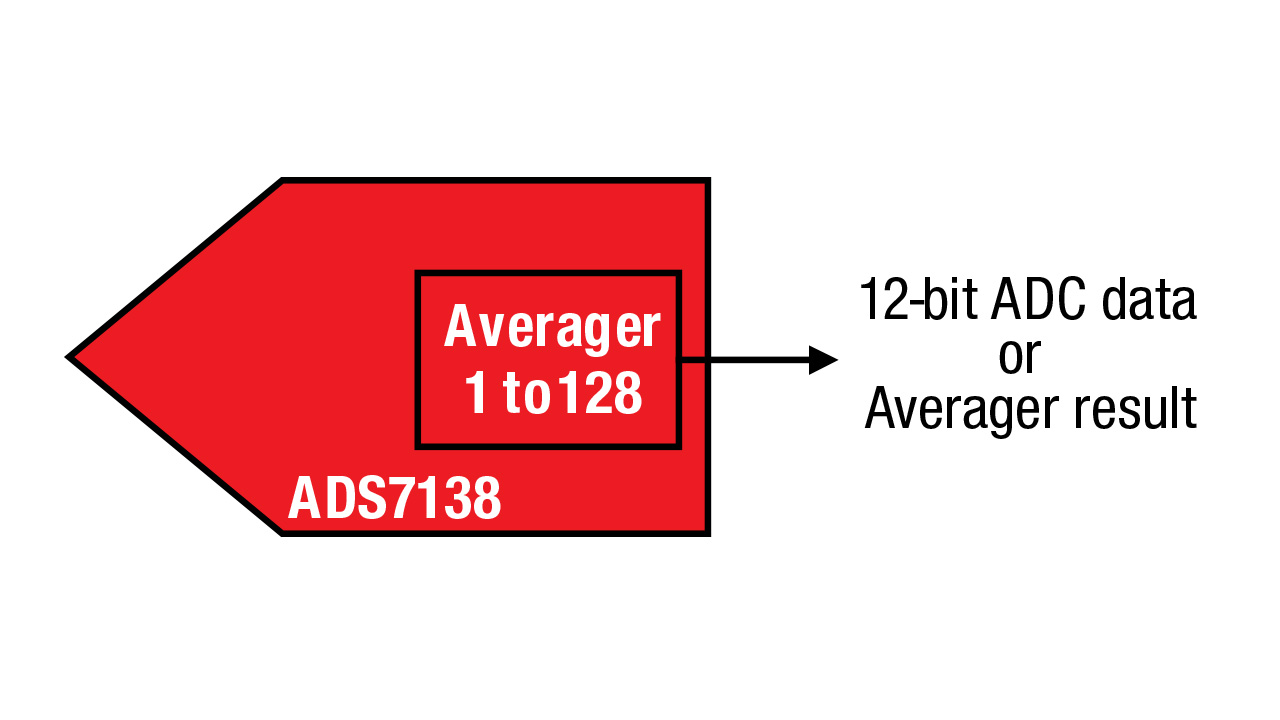
    It is a common practice to average sensor readings over a short period of time to reduce the effects of noise in the system. As shown in Figure 7, the ADS7138 can average as many as 128 samples, reducing the effects of noise by over 10 times.

Figure 7: Averaging feature inside ADS7138

  • General purpose input/output (GPIO)
    In many systems, the detection of an alarm event requires immediate control action (like switching off a heating element or turning on a hazard indicator). In the ADS7138, some of the analog input channels can monitor the sensors, while the unused analog input channels can serve as GPIO pins. As shown in Figure 8, the monitored sensor can control the status of GPIO pins locally, or a central processor using the I2C interface can control the status remotely.

Figure 8: ADS7138 as ADC and GPIO

  • Waveform generation
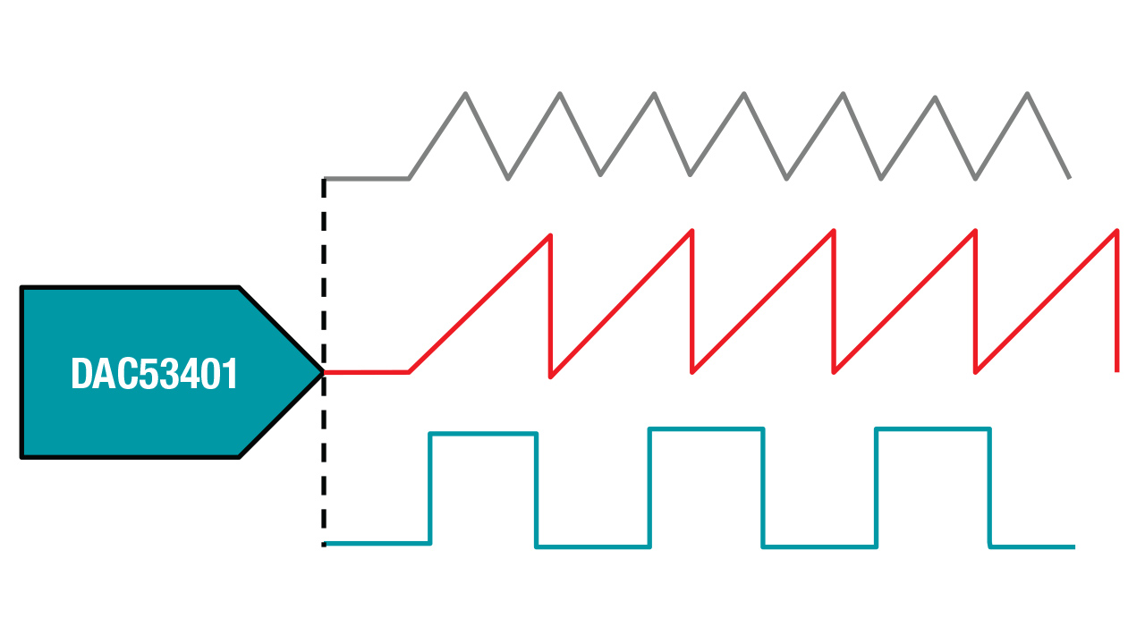
    In some systems, you need to generate certain waveforms to produce tones (like in medical applications) or create LED breathing effects (like in lighting applications). DACs like the DAC53401 come with a feature called continuous waveform generation, enabling you to generate triangle, square, trapezoidal or sawtooth waves, as shown in Figure 9.

Figure 9: DAC53401 generating multiple waveforms

  • Cyclic redundancy check (CRC)
    When using ADCs such as the ADS7138 for critical monitoring functions or redundant measurements, it becomes imperative to maintain data integrity. As shown in Figure 10, the ADS7138 achieves this by implementing CRC on the data communication between the ADC and the central processor.

Figure 10: ADS7138 with CRC on input and output data

As shown in Figure 11, DACs like the DAC53401 and DAC43401 use CRC to make sure that whatever is written to or loaded from the nonvolatile memory or EEPROM is not corrupted.

Figure 11: DAC53401 with CRC on NVM

Integrating these analog functions and digital features may lead to a more complex integrated circuit, but it can greatly reduce overall system complexity by adding processing and diagnostic capabilities.

Additional resources

Optimizing flip-chip IC thermal performance in automotive designs

$
0
0

Significant decreases in the size of power integrated circuits (ICs) have enabled system designers to achieve reductions in power-supply solution size and cost, which is imperative to furthering the development of advanced systems in the automotive industry. However, one challenge that arises from this trend is impaired thermal performance. Without a thoughtful printed circuit board layout to spread the heat, using smaller ICs in a design might result in a significant temperature rise, which is especially concerning for automotive applications.

One common small-size package is a flip-chip IC. Flip-chip packages have enabled ICs to become even smaller, making them a preferred choice for engineers designing tiny power-supply solutions. This size reduction has further impacted thermal performance, however, and made thermal mitigation even more challenging. In this article, I’ll review the considerations and guidelines for achieving optimal thermal performance with small flip-chip ICs.

The difference between standard wire-bond QFN and flip-chip packages

A typical package like a wire-bond quad flat no-lead (QFN) has a junction/die that typically connects to a thermal pad for heat dissipation, as shown in Figure 1. The junction has bond wires to connect the junction to the pins. The bond wires are very thin and do not conduct heat very well, resulting in most of the heat escaping from the thermal pad.

Figure 1: Junction connections to pins and thermal pad in a standard wire-bond QFN package

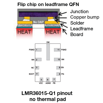
Flip-chip technology flips the chip/junction so that the copper bumps are upside down and soldered directly to the lead frame, as shown in Figure 2. This results in reduced parasitic impedances from the pin to the junction, improving efficiency, size, switch ringing and overall performance for a given specification. The flipped chip, however, prohibits the die from connecting directly to a thermal pad – there is no thermal pad on typical flip-chip devices. Fortunately, the elimination of the bond wires facilitates paths of high thermal conductivity from the die, through the pins and into the board. This results in good thermal conduction between the die and the board, thus removing heat from the IC.

Figure 2: Junction connections to pins for flip-chip devices

Using pins to optimize heat distribution

Power-supply designers can achieve very good thermal performance with flip-chip ICs by connecting and using flip-chip pins for heat distribution. Connecting the pins to large copper traces and polygon pours reduces the thermal resistance and pulls more heat out of the package.

The power ground (PGND) pin is often used to extract heat from the IC. PGND also requires higher current capability; therefore, the copper bump connecting the junction to the PGND pin is typically larger than the copper bump of a signal pin. This larger copper bump allows more heat to flow from the PGND pin(s). On the system side, PGND is electrically quiet, so a large copper surface area will not impact electromagnetic interference (EMI) levels – an important requirement in automotive systems.

You can use other pins for improved thermal performance, but take care not to increase the surface area of noisy nodes such as the switch node and the bootstrap pin, as this can impact EMI performance and may cause violations of EMI test limits.

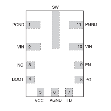
Let’s test these strategies using the LMR36015-Q1, a 150°C-rated, 60-VIN, 1.5-AOUT flip-chip buck converter. Figure 3 shows the pinout of the LMR36015-Q1.

Figure 3: Pin layout for the LMR36015-Q1

Pins 1 and 11 are PGND pins connecting to a large ground plane, which provides good heat distribution. The layout also uses thermal vias on the ground plane, harnessing the inner layers for even more heat distribution. Pin 6 is analog ground, which also has a large ground plane and thermal vias. Pins 2 and 10 are the input voltage (VIN) pins, which like the PGND pins have large internal copper bumps for increased current capacity and improved thermal conductivity for better heat dissipation. The input voltage on a buck is inherently noisy, however, so watch the size of the VIN plane in order to not push EMI levels past acceptable limits. The switch node and bootstrap pin are noisy due to fast changes in voltage, so it is important to keep those nodes as small as possible.

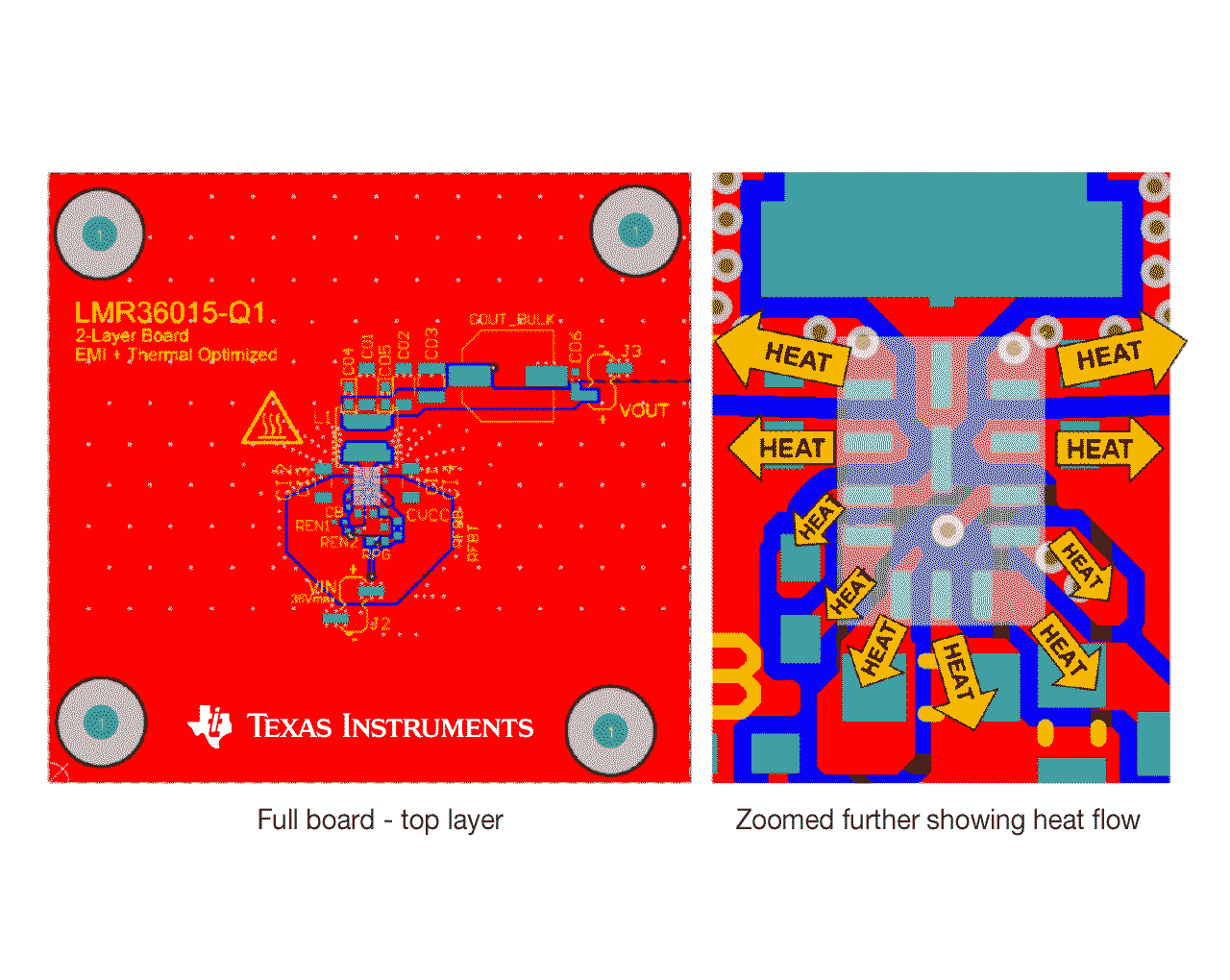
Figure 4 shows a thermally optimized layout of the LMR36015-Q1.

Figure 2: Sample layout for the LMR36015-Q1 flip-chip IC

The LMR36015-Q1 board measures 2.2 by 2.3 inches (5.6 cm by 5.8 cm) and only has two layers: top and bottom. Typical boards are larger and contain four or more layers, so the size and number of layers increases the thermal challenge. The thermally optimized layout allows the LMR36015-Q1 to operate at 12 VIN, 5 VOUT at a full load of 1.5 AOUT, switching at 400 kHz with a temperature rise of only 28°C in a 22°C still-air environment. This layout allows the 150°C-rated IC to operate in ambient temperatures as high as 115°C, which gives 10°C of margin above the 105°C ambient requirement, which is used in some of the harshest automotive environments.

Smaller-power ICs in flip-chip packages do not necessarily result in poor thermal performance. When compared to wire-bond packages, it is possible to achieve equivalent thermal performance by following the guidance presented in this article.

Additional resources

How current sensors help monitor and protect the world’s wireless infrastructure

$
0
0

Power amplifiers (PAs) play a critical role in the system architecture of wireless infrastructure. As the number of channels within active antenna systems (AASs) and remote radio units (RRUs) increase from four up to 128 and beyond with the expansion of 5G, the number of PAs is increasing at the same rate to support the multiple-input-multiple-output architecture of the AAS and RRU.

An increased channel count affects PA performance, since the system consumes more energy, thus increasing the temperature. Keeping the PA under control, meaning that current and temperature are kept within a specified safe operating range is directly related to device performance and longevity. To achieve system safety and efficiency, system designers are using various sensors to monitor activity in the PA.

In this article, I’ll review advancements in wireless infrastructure applications for high-voltage gallium nitride (GaN) or laterally diffused metal-oxide semiconductor (LDMOS) PAs in AAS and RRU systems for monitoring system vitals – in this case, current-sense amplifiers (CSAs).

Current sensors in PA current monitoring

There are several uses for current sensors to ensure the correct functionality and longevity of a PA, including calibrating, field maintenance and real-time monitoring. Monitoring the current going into a PA or a node enables the adjustment of its gate bias voltage in order to ensure that it is performing in the optimal range. CSAs such as TI’s INA293 offer very low offset and gain error along with high-voltage capability across the common mode, which is a good fit for high-side sensing where a high level of accuracy is required. With the INA293, you can directly take accurate measurements of a PA on a >48-VDC power supply.

During calibration of a PA in a factory (as illustrated in Figure 1), a look-up table is created by monitoring current by using one CSA per PA or one CSA per two PAs. The amount of CSAs depends on board space and the level of accuracy required. Using a single CSA per PA will provide the most accurate data, since the current data isn’t being averaged across several PAs.Correct calibration of the PA in the factory is essential to longevity of the device and performance in the field.


Figure 1: Factory calibration

Maintaining and adjusting the AAS and RRU PAs after systems deployment is another implenmention for a CSA because the system may need adjustments over time as components wear and break down. When systems are deployed into environments with large temperature deltas, the CSA can help adjust the gate voltage of the PA to ensure optimal performance throughout changing weather conditions. With this adjustment technique, the system needs to be powered off and then recalibrated remotely by monitoring current entering the PA during a remote calibration cycle. Adjusting the voltage gates of the PA accordingly ensures proper operation and the highest efficiency.

Continually monitoring a device in real time is another way to analyze PA performance. In this case, the CSA is providing data to a digital-to-analog converter (DAC), which is controlling the LDMOS or GaN device by adjusting the gate voltages in real time. Enabling the adjustment of the gate voltage in real time will result in optimal performance and power consumption in all operating conditions and load levels. This technique does not require taking the system offline to adjust the gate voltages, since there is a real-time communication channel directly to the processor that makes any necessary adjustments. Adjusting the gate voltages in real-time is a design challenge, however, because you’ll need to create complex algorithms or an application-specific integrated circuit to handle the data from the DAC.

System protection and consumption

It is important to protect the PA from overcurrent situations, since it is one of the most expensive components in the system. Placing a CSA on the high-side of a PA equipped with a fast-action internal comparator such as the INA202 that offers a typical response time of 1.3 µS and a common-mode voltage range up to 80 V. This solution provides overcurrent detection to ensure that the PA is not damaged due to a high current event. A digital power monitor such as the INA226 can monitor power being delivered to the PA to ensure that the PA stays within technical operating specifications throughout its lifetime and operates correctly in various environments. The INA226 monitors current, voltage and power and provides user alerts, which are then sent through the I2C interface for reliable communication with a processor.


Figure 2: System protection configuration

Power delivery and power supplies

A high-voltage AC power sourced from the electrical grid provides power to a wireless infrastructure base station. It is important to monitor the high-voltage AC coming from the power grid to ensure that the system does not experience a condition such as a power surge or outage, which may damage components in the power supply and prohibit the system from operating correctly.

To monitor high AC voltages <600 Vpk, TI’s TMCS1100 and TMCS1101 devices have a maximum total error of <1% or <1.5%, respectively, and isolation from high voltages. In addition, the TMCS1100 and TMCS1101 are very stable over a temperature range, making them a good fit for outdoor systems. Adding this device to a system is an additional layer of protection for the system, making sure that it is correctly sourcing AC power.

For DC/DC converters, the INA240 provides enhanced pulse-width modulation rejection and bidirectional operation. This means that the device will avoid glitches in the current measurements from sharp common-mode transitions, which leads to accurate measurements. Depending on the converter’s power levels, thermal generation or heat can manifest quickly. The INA240 has a low thermal drift specification, which means that the current measurement does not change significantly with heat generation, ultimately providing accurate measurements throughout the entire operating range.

Conclusion

Current sensing provides many benefits to a system, including optimized performance, efficiency, improved reliability and condition monitoring to protect system vitals. Since CSAs enable direct measurements with highly accurate results, they they can help extend the reliabitliy and life of PAs while supporting a variety of functions and features in a system.

Additional resources:


Going crystal-less is easy with the world's first crystal-less, wireless SimpleLink™ MCU

$
0
0
  Innovation in the semiconductor industry is often about adding on to an existing product, but less is more when it comes to design. At TI, we looked at the electronic build of materials (BOM) surrounding our SimpleLinkTM wireless MCUs and dec...(read more)

Motor-driven automation in smart home systems: how to achieve efficiency and cost savings

$
0
0

My last technical article, “Automating smart home systems with motor drivers,” explored how motorized applications like video doorbells and smart locks provide a sense of security and convenience. In this article, I’ll cover how motorized systems in window blinds and smart thermostats can help make heating, ventilation and air-conditioning (HVAC) systems more efficient and reduce overall energy costs.

Smart thermostats

Smart thermostat manufacturers claim upwards of 25% energy and cost savings on HVAC system expenses compared to traditional thermostats. These savings are possible because smart thermostats adapt to usage patterns, which optimize when the HVAC is on or off. Remote control via wireless connectivity is another factor behind the growth of smart thermostats. For example, consumers can turn on their AC when commuting home from work and arrive to a cool house.

Traditional thermostats use electromechanical relays to switch power on and off to HVAC compressors, fans, evaporators, the furnace and other parts of the system. The loud clicking noise when the AC turns on is from the traditional relay actuating. There is virtually no audible noise coming from a metal-oxide semiconductor field-effect transistor (MOSFET) H-bridge integrated circuit (IC). Because electromechanical relays have large contacts, they are also typically larger compared to ICs, taking up some serious board space.

Another major flaw with traditional electromagnetic relays is their limited number of actuations – and thus, their life span. A typical relay has between 50,000 to 100,000 cycles, so in buildings designed to last a lifetime or more, relays may not be the best solution. In comparison, actuation with an H-bridge is in the order of multiple millions or more cycles, as long as there is protection from overheating and overcurrent events. Devices like TI’s DRV8837 and DRV8837C<12-V H-bridge driver and DRV8876<40-V H-bridge driver include the necessary protections.

Another not-so-obvious way to use an H-bridge motor driver like the DRV8837C is to drive a piezo speaker or buzzer in a thermostat. Piezo buzzers are commonly used as an audible feedback mechanism when programming the thermostat or changing the temperature. In its basic architecture, a piezo buzzer is a disk of piezoelectric material with electrodes connected to both faces of the disk. Applying a voltage deforms the disk, creating sound in the buzzer. Depending on the configuration of the OUT1 and OUT2 pins of the DRV8837C, applying a positive or negative voltage to the electrodes gives full range of the piezo speaker, as shown in Figure 1.


Figure 1: A piezo buzzer driven by DRV8837C outputs

Some thermostat models have a rotary dial controlled by a small motor, while the temperature is set remotely from a smart home app. A brushed-DC motor with positional feedback can be a good fit, with the DRV8837C driving the motor to a specified dial position. A stepper motor driver like the DRV8847 can drive this motor in full step mode with only two general-purpose inputs/outputs (GPIOs), whereas most drivers require four GPIOs.

Motorized window blinds, shades, shutters and curtains

According to the U.S. Department of Energy, in the warmer seasons, “76% of sunlight that falls on double-pane windows becomes heat.” Equipping a home or office with motorized blinds that can adapt to temperature, changing seasons, the sun’s various positions and other variables is an excellent way to reduce cost and energy usage of HVAC systems.

A couple of different motor-driver topologies are suitable for raising and lowering blinds, depending on the load’s weight, desired efficiency and overall system complexity. For small blinds or individual installations, a motor driver with integrated MOSFETs will help keep overall system size and bill of materials (BOM) small. For heavier loads or to better distribute heat dissipation, a gate driver with external MOSFETs enables higher performance and greater flexibility by choosing the on-resistance of the MOSFET’s RDS(on) according to how much current and torque the blinds, shutters, shades or curtains require.

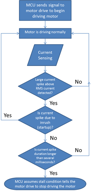
One other important aspect of the motor driver in these systems is current sensing and regulation. In brushed-DC-driven systems, when the motor starts up there is a spike of current, sometimes called inrush current. A large inrush current can draw too much power away from the battery, limiting supply to other critical parts of the system. The motor’s torque is also dependent on the amount of current delivered to the motor. The ability to sense and regulate current with a motor driver can enable torque control.

Another benefit of current sensing is the detection of stall conditions in the motor. When the blinds or shades reach an end-of-travel point or mechanical stop, the current in the motor will rise to a level typically much higher than the continuous current required during steady motion. By measuring the current and sending a scaled-down analog signal back to the microcontroller’s analog-to-digital converter (ADC), the microcontroller can detect this drastic change in current, assume a stalled position, and stop sending a drive signal to the motor driver, as shown in Figures 2 and 3.


Figure 2: Flow chart of a microcontroller and motor-drive operation during a stall event


Figure 3: A typical motor current profile during startup (inrush) current, continuous current and stall event current

The DRV8876 (3.5-A peak) and DRV8874 (6-A peak) are mid-voltage-range, integrated MOSFET motor drivers with integrated current sensing and feedback (through the IPROPI pin). The DRV8873 integrated MOSFET motor driver has the same integrated current sensing and feedback (IPROPI) features, but 150-mΩ RDS(on) MOSFETs enable a higher peak current of 10 A, which means that the device will work well for heavier blinds and shades with more torque capability.

For even heavier types of motorized blinds, shades, shutters and curtains, a gate driver like the DRV8701 is a good fit. You can select the RDS(on) of the external MOSFETs depending on the appropriate amount of current needed to drive the load. Separating the gate driver from the MOSFETs also more evenly spreads heat dissipation. The DRV8701 has an integrated current-shunt amplifier with an output pin that can send the sensed current back to the microcontroller to detect a stall, as shown in Figure 4.


Figure 4: The DRV8876 integrated MOSFET driver and DRV8701 gate driver for brushed-DC motors, with integrated current sensing and feedback

Smart home systems often have connectivity features to control subsystems wirelessly. Brushed-DC motors can generate noise on these communication lines and cause interference in these systems. By controlling the slew rate of the MOSFETs’ switching, it’s possible to achieve a balanced trade-off between electromagnetic interference radiation and thermal dissipation. The DRV8701 has smart gate drive technology from TI that integrates this slew rate control function. Normally this is a discrete circuit between the gate driver and the MOSFETs (Figure 5). Smart gate drivers enable more robust performance without having to increase the BOM cost and board size.


Figure 5: A half-bridge discrete solution for slew rate control vs. TI’s smart gate drive

Whether a home or office building has smart locks, video doorbells, smart thermostats, motorized window closures or other motor- and H-bridge-driven systems, TI has several motor drive devices and technologies to enhance system performance and reliability while reducing cost and size.

Additional resources

Making ADAS technology more accessible in vehicles

$
0
0

Advanced driver assistance system (ADAS) features have been proven to reduce accidents and save lives. According to Consumer Reports, the Insurance Institute for Highway Safety shows that there were 50% fewer front-to-rear crashes with vehicles equipped with forward-collision warning and automatic emergency braking technology compared to cars without these systems in 2017. Tragically, most accidents happen to drivers whose cars are not equipped with even the simplest ADAS applications.

As ADAS continues to evolve toward the Society of Automotive Engineers-defined L4 and L5 autonomous vehicles, there’s an opportunity to make a greater impact on the road by creating ADAS technology that can be used in a wider range of cars.

Although it is not economically practical for all cars to have all ADAS technology, the objective should be to make driving assistance features available in as many cars as possible. This means that more vehicles on roads need to be capable of cost-effectively sensing, processing and acting on real-time data.

The need for smart and diverse sensing

Feature-based computer vision algorithms have traditionally handled the analysis of image data collected for ADAS operations. Computer vision has served the industry well over the last decade, but as ADAS operations become more advanced, designers need additional tools to handle and adapt to situations that drivers and their vehicles face on the road.

Maintaining consistent ADAS operations in all situations is challenging. Unanticipated scenarios like the sudden onset of inclement weather or unsafe road conditions require vehicles to adapt in real-time. These are not scenarios you can code for, but by developing a dynamic system that can help the car sense, interpret and react quickly to the world around it, cars can act more like a co-pilot for the driver. Such a system requires data and the ability to process that data in real-time using a combination of computer vision and efficient deep learning neural networks.

ADAS solutions need to extract data from a diverse sensor set and convert the data to actionable intelligence for the vehicle. At a minimum, these sensors include different types of cameras and associated optics, radars and ultrasonic technology. More complex cases will also include LiDAR and thermal night vision. Further, the system may perform vehicle localization by comparing features extracted from sensor data with high-definition map data. Assimilating and analyzing this multimodal sensor data must happen in real-time – new data arrives 60 times per second – without replacing the backseat of a car with a data-center server.


Enhance automated parking with Jacinto™ processors.


Learn more.

Any solution must be road-ready

In the same way that a driver receives multiple inputs concurrently and must make a safe driving decision quickly, any ADAS application — no matter what the level of autonomy – must do the same. A high-performance system on chip (SoC) that can handle concurrent processing without blowing the budget in terms of power, heat, component and integration costs is highly desirable. An SoC solution can scale from more simple cases (fewer sensors, lower resolutions) to the most complex cases without compromising basic ADAS features or requiring a lower-end system.

Meeting application performance across a vehicle lineup is only one requirement. For wide deployment, these systems must be developed cost-effectively. Software complexity is increasing exponentially in vehicles – it is already 150 million lines of code – which is exploding development and maintenance costs. As systems become more situationally aware, safety requirements will evolve and grow, and all of these systems must meet strict automotive quality and reliability targets. These are the exacting demands and realities of supporting the automotive electronics market.

The right SoC addresses all of these demands. It can properly balance memory, inputs/outputs and processing cores against a range of application demands, helping meet system bill-of-materials targets. The right SoC can also accommodate an open software development methodology, making it possible to reuse the resulting code and preserve efforts made in development and testing. An SoC can also be built from the beginning with functional safety as an imperative and with the reliability and product longevity necessary to keep vehicle lines viable in the market for years. Done well, the vision of enabling more cars with robust ADAS features (like those shown in Figure 1) is within reach.

Figure 1: Examples of ADAS applications

How TI is helping democratize ADAS technology

TI worked to address sensing, concurrent operation and system-level challenges by leveraging our decades of automotive and functional safety expertise to design our Jacinto 7 processor platform.

We focused on what matters to the entire system: combining outstanding sensing capabilities that monitor a car’s surroundings in multiple directions, and using an automotive-centric design methodology for optimized power and system cost.

The new Jacinto 7 processor family, including the TDA4VM and DRA829V, integrates key functional safety features on-chip that enable both safety-critical and non-safety-critical functions on one device; they also improve data management by incorporating high-speed and automotive interfaces. Jacinto 7 processors bring real-world performance to automotive ADAS and gateway systems and help lower system costs to help democratize ADAS technology and make it more accessible.

Enabling the software-defined car with a vehicle compute gateway platform

$
0
0

There are three clear automotive trends: the migration to semi-autonomous and autonomous vehicles, vehicles connected to the cloud with increasing data bandwidths, and vehicle electrification. These trends are driving changes to vehicle architectures. The current vehicle architecture is an ever-increasing number of engine control units (ECUs) connected by low-speed Controller Area Network (CAN)/Local Interconnect Network (LIN) communication buses. This architecture has several limitations, however. 

For example, software development, maintenance and validation are complex. Each ECU has software written by a different supplier. For vehicle systems to operate effectively, software must be aligned across systems in the car. Adding features to an existing system can be a complicated, slow and error-prone process. Achieving autonomy and connectivity by adding new functionalities and capabilities to vehicles is difficult or impossible to implement with distributed ECUs. 

Semi-autonomous and autonomous vehicles require the use of multiple cameras, radars and LIDAR. Communicating all of that raw data around the vehicle requires many ECUs to be able to handle Gigabit Ethernet. Processing raw data and drawing conclusions drives up the processing requirements and cost. Vehicle electrification currently requires batteries that can be expensive, making it challenging to stick within system budgets. 

The first step toward overcoming these challenges is to centralize functions into functional domains that support actions either a section of the car or for a particular function of the car (ex: HEV/EV operations). Figure 1 shows an example of a vehicle compute architecture that incorporates functional domains. Functional domains act as a gateway between the high-bandwidth interconnect to other domains and the lower-bandwidth CAN/LIN interconnect of the remaining domain ECUs. Decreasing the number of ECUs, the amount of wiring in the vehicle and the number of connectors helps achieve significant cost savings. Limiting high-bandwidth data processing to the functional domains minimizes the complexity and cost of the sensors and actuators in the remaining ECUs. Implementing software features/applications in the functional domains only (rather than being distributed over multiple ECUs and suppliers) enables a structured software development process. 


Figure 1: Automotive gateway vehicle compute architecture 

There is an emerging trend to create a software-defined vehicle through an architecture comprising one to three vehicle compute platforms per vehicle that integrate functionality. A critical enabler of the software-defined vehicle is the employment of a service-oriented architecture (SOA). SOA systems consist of loosely couple services that communicate through simple interoperable interfaces to distinct functions, typically over a network.

Some benefits of SOA include hardware independence, simplified testing, faster deployment and cross-discipline application development. A note on that last point: Since services are presented as black boxes with abstract interfaces, it’s not necessary to use the same technology or even the same supplier to implement each service. 

SOAs have a long history in other markets, such as web services, software as a service and platform as a service (aka cloud computing). An automotive example is a simple ECU that provides tire pressure information. Multiple applications use tire pressure data: one may be a human machine interface displaying current vehicle information; another may be a mph calculator that itself feeds an electric vehicle battery manager. It is possible to replace the tire pressure ECU using a different hardware vendor or for it to be integrated into a larger, multifunction ECU. Because upstream applications use an abstract interface to the ECU’s services, they are not affected by a change in ECU or integration into another ECU when using an SOA. In the tire pressure example, the components supporting the tire pressure sensor system can be from different companies or use different sensing technologies because the tire pressure data is aggregated in smaller ECU.


Vehicle compute gateway platforms clearly increase the compute requirements per platform, which can use one or multiple compute system on chips (SoCs) depending on the processing required. Compute SoCs have to efficiently share data between them. Peripheral Component Interconnect Express (PCIe) is a high-bandwidth backbone that interconnects the compute SoCs and mass storage, while Gigabit Ethernet is the high-bandwidth communication from the vehicle compute platform to the rest of the vehicle. 

TI’s DRA829V application processor is the first processor to integrate a PCIe switch on-chip to share high bandwidth data between the compute processors to enable faster high-performance processing. The PCIe switch integrated into the DRA829V efficiently moves data between the SoCs. There is no need for central processing unit intervention or temporary storage. 

Because the vehicle compute platform must be able to manage data communication with the rest of the vehicle, the DRA829V processor includes an eight-port, Gigabit Ethernet switch to communicate outside the box, along with the multiple traditional automotive CAN-Flexible Data Rate/LIN interfaces for communicating to the rest of the vehicle. 

There are functional safety requirements for a portion of the functions. The DRA829 leverages more than 20 years of functional safety experience to support mixed criticality processing. Lockstep Arm® Cortex™-R5Fs enable ASIL- D while the entire SOC is ASIL-B capable. Extensive on chip firewalls enable the freedom from interference required to manage mixed criticality safety and non-safety functions simultaneously. Figure 2 compares a typical vehicle compute platform with one using the DRA829V. The DRA829V requires half as many packages saving cost, power and physical size.


Figure 2: Two examples of vehicle compute gateway systems

Automotive vehicle architectures are evolving to meet the demands of the industry trends. There is emerging vehicle architecture to enable the software defined vehicle based on a SOA, which means one to three vehicle compute platforms are needed per vehicle. TI’s new DRA82x family of processors was purpose-built for these requirements and help automakers and Tier-1 suppliers efficiently develop vehicle compute platforms that meet system needs and system cost constraints.

Next-generation battery monitors: how to improve battery safety while improving accuracy and extending runtime

$
0
0

In recent years, consumer products like vacuum cleaners, power tools (such as drills, saws and screwdrivers) and garden tools (like mowers, edgers and lawn tractors) have moved from being corded and wall-powered to cordless and operating from rechargeable battery packs. Even previously unpowered devices like bicycles are now transitioning to battery-powered e-bikes and e-scooters.

These battery packs, which are typically constructed from individual lithium-ion, lithium-polymer or lithium-phosphate cells, can be dangerous if used incorrectly, resulting in fires or explosions. To ensure their safe use, electronics included within the pack monitor the cells so that they only operate under conditions specified by the cell manufacturer. These conditions typically include:

  • The maximum allowed charging voltage.
  • The maximum charging and discharging currents.
  • A specified temperature range for charging and discharging.

Thus, the measurement of key parameters within the battery pack is critical, especially the voltage, current and temperature of the cells in the pack, as this data will trigger appropriate protective actions when the parameters exceed the limits.

The measurement data must be accurate so that designers can determine how much margin to include in a design. For example, if a cell specification limits the full charging voltage to 4.3 V but the measurement data has an accuracy of ±50 mV, then the designer must configure the system to disable charging whenever the measurement indicates a voltage above 4.25 V. Since the actual cell voltage may be as low as 4.2 V, however, in this case charging would stop before the cell was fully charged, resulting in wasted capacity and a shorter battery life for the application.

High-accuracy battery monitors and protectors for battery packs, like the BQ76942 and BQ76952, are designed especially for applications using lithium-ion, lithium-polymer or lithium-phosphate cells. Supporting series stacks of batteries from 3s up to 10s (the BQ76942) and 16s (the BQ76952), these devices measure cell voltage, current and temperature, and can share data with other circuitry, such as a separate microcontroller within a battery pack or the system controller in an e-bike. The BQ76942 and BQ76952 can also use the data to autonomously trigger battery protection, disabling a battery pack to avoid operation outside manufacturer specifications and re-enabling the pack again when conditions permit, with or without interacting with a host or system microcontroller.

Figure 1 shows the block diagram for the BQ76952, which integrates:

  • Measurement and detection subsystems, which monitor voltages, current and temperature to detect when a parameter exceeds an allowed threshold.
  • Actuators for driving external protection FETs and a chemical fuse.
  • A digital host interface subsystem, supporting several serial communications standards, in addition to pin controls for select functions.
  • Multiple voltage regulators, one for internal circuitry, and two for external use.

Figure 1: Block diagram of the BQ76952

Figure 2 shows a simplified schematic of a 16s battery pack based on the BQ76952, using I2C for communication with a host microcontroller. The integrated regulators provide supply rails for the microcontroller and an optional external transceiver.

Figure 2: Simplified schematic of a 16s system based on the BQ76952

The measurement subsystem in the BQ76942 and BQ76952 digitizes various voltages, current and temperature within the battery pack. These measurements are obtained in different ways, due to the specific requirements for each. For example, temperature varies slowly, so it can be measured and calculated at slow intervals. However, pack current may have short bursts of activity, which can be missed if not sampled continuously.

The values generated by voltage and Coulomb-counter ADCs are processed to provide the measurement data, which is used within the device and made accessible to a separate processor within the battery pack or to the system controller in the power tool or e-bike. This data includes:

  • Differential voltage of individual cells and select additional system voltages.
  • Pack current and passed charge (Coulomb count).
  • Internal die and up to nine external thermistor temperature readings.

Pins supporting external thermistor measurement can also be used for general-purpose ADC inputs, supporting input voltages up to ~1.8 V. The voltage ADC operates on a measurement loop, with the input multiplexed among several inputs on a periodic basis. The measurement subsystem of the BQ76942 and BQ76952 includes several programmable options to allow optimization and trade-offs between measurement speed and accuracy.

As battery-powered consumer products continue to become more prevalent, ensuring they operate within safe voltage, current and temperature ranges is essential. Battery monitors with integrated functionality can help design engineers address these three key concerns while improving accuracy. For more information about designing with TI battery monitors, please review our additional resources below.

Additional resources

Viewing all 4543 articles
Browse latest View live


<script src="https://jsc.adskeeper.com/r/s/rssing.com.1596347.js" async> </script>