Quantcast
Channel: TI E2E support forums
Viewing all 4543 articles
Browse latest View live

Why current and magnetic sensing matters for wireless earbud design

$
0
0

Wireless earbuds have infiltrated the electronics market in recent years. Users can now walk away from their streaming devices without the fear of being yanked back by a caught wire. True wireless earbuds are Bluetooth®-based wireless earbuds that have their left and right channels separated into individual housings. And while this innovation has freed consumers from having to be connected to their phones by a wire, it has also presented a host of new design challenges for earbud manufacturers.

To maximize battery life and support long battery runtime, it’s important to ensure an efficient charge with the earbuds seated properly in their charging case. Magnetic sensors helpensure proper earbud seating because they use magnets to detect fine object movements. Commonly, using current-sense amplifiers for earbud charging and Hall-effect switches for wireless charging cases support maximium battery charge and battery life for these applications.

Designing with current-sense amplifiers

The batteries in wireless earbuds are often in the sub 100-mAh range. Therefore, better current measurement is necessary in order to protect and accurately charge these smaller-capacity cells. Traditional battery chargers and gauges do an excellent job of monitoring larger currents for batteries like those in a charging case, but often do not fare well at super-low currents.

Dedicated current-sense amplifiers are more accurate when measuring small currents. If you already have a microcontroller (MCU) or power-management integrated circuit (PMIC) in your design, you can use the output of these amplifiers to monitor and gauge battery use times and lifetimes based on algorithms written in the MCU or PMIC.Figure 1 shows a battery fuel gauge with an external current-sense amplifier and controller.


Figure 1: Battery fuel gauging with an external current-sense amplifier and controller

Placing two small-size current-sense amplifiers like the INA216 in a wireless earbud charging case will enable highly accurate charging current measurements. Alternatively, if solution size is a priority, using a single dual-channel-capable current-sense amplifier like the INA2180 is recommended.

If accuracy is less important, and assuming an equal current division, one current sensor can monitor charging in both earbuds. Placing bidirectional-capable current-sense amplifiers like the INA191 or INA210 in the earbuds themselves will enable both charging and gauging functionalities. Regardless of which topology you choose, these devices can also enable better battery protection, as even small changes in current can affect battery lifetimes.

Designing with Hall-effect sensors

A new feature of wireless earbuds is lid and charge detection within their companion charging cases. Charging cases must be able to detect the position of the lid and be able to detect the presence of the earbuds inside the case for charging. Other sensor technologies may not have the ability or sensitivity to discern these things correctly in a cost-effective manner, so choosing the right sensor is crucial. Figure 2 shows wireless earbud sensor placement.


Figure 2: Wireless earbud sensor placement and use

Hall-effect sensors work well for charging case lid and earbud charge detection. Magnets are already used to clasp charging case lids shut, so using a magnetic sensing solution for lid detection in the form of Hall-effect switches is an obvious solution that requires no extra parts. In addition, placing magnets in the earbuds themselves enables a robust means of detecting whether the earbuds are present inside their charging case. Knowing whether the earbuds are in or out of the case will allow Bluetooth auto-connect when the earbuds are removed, or charge detection when they are inside the case.

Choosing the right digital Hall-effect sensor is important, and features such as low frequency and low power make the DRV5032 a good fit. For Hall-effect sensor applications in earbuds, providing magnet detection information five times per second is more than enough. This frequency allows you to use the DRV5032’s low-power option, which consumes only about 0.5 µA and does not place a significant drain on the device’s battery.

Determining state of charge and charging case lid detection are both critically important to earbuds with their small-capacity batteries and wireless connectivity. Current-sense amplifiers and Hall-effect sensors provide a solution for those struggling to design around these new features and challenges.

Additional resources


Get more out of your power supply with port power management

$
0
0

With the publication of the new Institute of Electrical and Electronics Engineers 802.3bt standard, the power range of Power over Ethernet (PoE) loads continues to expand. If you are designing systems that provide PoE, this presents a challenge. You may need to provide 5 W of power to a low-end Internet Protocol camera or 70 W to a high-end wireless access point (WAP). An enterprise switch with 48 ports that can simultaneously support 90 W on all ports would require a 4.3-kW supply.

You probably want to enable the full functionality of the high-end WAP, but do you really want to pay for the giant power supply? Knowing the typical use case of your system, you can choose a smaller power supply that would be sufficient in most situations. But, how do you prevent the supply from overloading in the rare event that all loads draw full power?

Port power management (PPM) algorithms can come to your rescue. When a new device is plugged in, the system will only turn the device on if there is enough remaining power. A system that supports priority and exceeds its power budget will actually shut down a lower-priority load when a higher-priority load is plugged in.

At a high level, PPM is a simple concept, but it can have multiple flavors, and its implementation can be tricky. Typically, there are multiple power sourcing equipment (PSE) devices, thus requiring a central microcontroller (MCU) to manage the system. Also, the system could have slots for multiple power supplies, which can get plugged in or unplugged during operation.

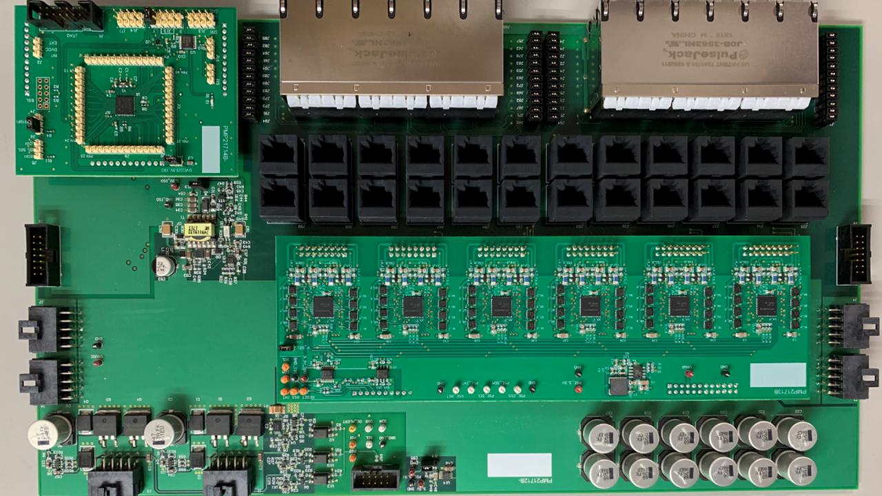
TI’s FirmPSE ecosystem can give you a huge head start in implementing PPM in your end equipment by removing the burden of writing low-level code to control the PSEs. Figure 1 shows the evaluation board of TI’s FirmPSE, which is implemented using an MSP430™ MCU and TPS23881 PSE. TI provides a binary image that you can load directly into the MSP430F5234. You will need to write code that interfaces between the host central processing unit (CPU) and the MSP430F5234 to configure the system and monitor the port status.

 Evaluation board of TI’s FirmPSE ecosystem

Figure 1: Evaluation board of TI’s FirmPSE ecosystem

TI’s ecosystem features:

  • Orderable TI designs with twenty-four 90-W PoE ports.
  • A user’s guide.
  • A binary image that can be loaded directly to the MCU.
  • A host interface document defining the interface between the MSP430F5234 and host CPU.
  • A graphical user interface to configure the binary image and to evaluate monitor port status’s of the FirmPSE system.


To learn more about PPM and ways to reduce your power supply consider watching our FirmPSE system firmware GUI offline mode or online mode training videos.

Making ADAS technology more accessible in vehicles

$
0
0

Advanced driver assistance system (ADAS) features have been proven to reduce accidents and save lives. According to Consumer Reports, the Insurance Institute for Highway Safety shows that there were 50% fewer front-to-rear crashes with vehicles equipped with forward-collision warning and automatic emergency braking technology compared to cars without these systems in 2017. Tragically, most accidents happen to drivers whose cars are not equipped with even the simplest ADAS applications.

As ADAS continues to evolve toward the Society of Automotive Engineers-defined L4 and L5 autonomous vehicles, there’s an opportunity to make a greater impact on the road by creating ADAS technology that can be used in a wider range of cars.

Although it is not economically practical for all cars to have all ADAS technology, the objective should be to make driving assistance features available in as many cars as possible. This means that more vehicles on roads need to be capable of cost-effectively sensing, processing and acting on real-time data.

The need for smart and diverse sensing

Feature-based computer vision algorithms have traditionally handled the analysis of image data collected for ADAS operations. Computer vision has served the industry well over the last decade, but as ADAS operations become more advanced, designers need additional tools to handle and adapt to situations that drivers and their vehicles face on the road.

Maintaining consistent ADAS operations in all situations is challenging. Unanticipated scenarios like the sudden onset of inclement weather or unsafe road conditions require vehicles to adapt in real-time. These are not scenarios you can code for, but by developing a dynamic system that can help the car sense, interpret and react quickly to the world around it, cars can act more like a co-pilot for the driver. Such a system requires data and the ability to process that data in real-time using a combination of computer vision and efficient deep learning neural networks.

ADAS solutions need to extract data from a diverse sensor set and convert the data to actionable intelligence for the vehicle. At a minimum, these sensors include different types of cameras and associated optics, radars and ultrasonic technology. More complex cases will also include LiDAR and thermal night vision. Further, the system may perform vehicle localization by comparing features extracted from sensor data with high-definition map data. Assimilating and analyzing this multimodal sensor data must happen in real-time – new data arrives 60 times per second – without replacing the backseat of a car with a data-center server.


Enhance automated parking with Jacinto™ processors.


Learn more.

Any solution must be road-ready

In the same way that a driver receives multiple inputs concurrently and must make a safe driving decision quickly, any ADAS application — no matter what the level of autonomy – must do the same. A high-performance system on chip (SoC) that can handle concurrent processing without blowing the budget in terms of power, heat, component and integration costs is highly desirable. An SoC solution can scale from more simple cases (fewer sensors, lower resolutions) to the most complex cases without compromising basic ADAS features or requiring a lower-end system.

Meeting application performance across a vehicle lineup is only one requirement. For wide deployment, these systems must be developed cost-effectively. Software complexity is increasing exponentially in vehicles – it is already 150 million lines of code – which is exploding development and maintenance costs. As systems become more situationally aware, safety requirements will evolve and grow, and all of these systems must meet strict automotive quality and reliability targets. These are the exacting demands and realities of supporting the automotive electronics market.

The right SoC addresses all of these demands. It can properly balance memory, inputs/outputs and processing cores against a range of application demands, helping meet system bill-of-materials targets. The right SoC can also accommodate an open software development methodology, making it possible to reuse the resulting code and preserve efforts made in development and testing. An SoC can also be built from the beginning with functional safety as an imperative and with the reliability and product longevity necessary to keep vehicle lines viable in the market for years. Done well, the vision of enabling more cars with robust ADAS features (like those shown in Figure 1) is within reach.

Figure 1: Examples of ADAS applications

How TI is helping democratize ADAS technology

TI worked to address sensing, concurrent operation and system-level challenges by leveraging our decades of automotive and functional safety expertise to design our Jacinto 7 processor platform.

We focused on what matters to the entire system: combining outstanding sensing capabilities that monitor a car’s surroundings in multiple directions, and using an automotive-centric design methodology for optimized power and system cost.

The new Jacinto 7 processor family, including the TDA4VM and DRA829V, integrates key functional safety features on-chip that enable both safety-critical and non-safety-critical functions on one device; they also improve data management by incorporating high-speed and automotive interfaces. Jacinto 7 processors bring real-world performance to automotive ADAS and gateway systems and help lower system costs to help democratize ADAS technology and make it more accessible.

Enabling the software-defined car with a vehicle compute gateway platform

$
0
0

There are three clear automotive trends: the migration to semi-autonomous and autonomous vehicles, vehicles connected to the cloud with increasing data bandwidths, and vehicle electrification. These trends are driving changes to vehicle architectures. The current vehicle architecture is an ever-increasing number of engine control units (ECUs) connected by low-speed Controller Area Network (CAN)/Local Interconnect Network (LIN) communication buses. This architecture has several limitations, however. 

For example, software development, maintenance and validation are complex. Each ECU has software written by a different supplier. For vehicle systems to operate effectively, software must be aligned across systems in the car. Adding features to an existing system can be a complicated, slow and error-prone process. Achieving autonomy and connectivity by adding new functionalities and capabilities to vehicles is difficult or impossible to implement with distributed ECUs. 

Semi-autonomous and autonomous vehicles require the use of multiple cameras, radars and LIDAR. Communicating all of that raw data around the vehicle requires many ECUs to be able to handle Gigabit Ethernet. Processing raw data and drawing conclusions drives up the processing requirements and cost. Vehicle electrification currently requires batteries that can be expensive, making it challenging to stick within system budgets. 

The first step toward overcoming these challenges is to centralize functions into functional domains that support actions either a section of the car or for a particular function of the car (ex: HEV/EV operations). Figure 1 shows an example of a vehicle compute architecture that incorporates functional domains. Functional domains act as a gateway between the high-bandwidth interconnect to other domains and the lower-bandwidth CAN/LIN interconnect of the remaining domain ECUs. Decreasing the number of ECUs, the amount of wiring in the vehicle and the number of connectors helps achieve significant cost savings. Limiting high-bandwidth data processing to the functional domains minimizes the complexity and cost of the sensors and actuators in the remaining ECUs. Implementing software features/applications in the functional domains only (rather than being distributed over multiple ECUs and suppliers) enables a structured software development process. 


Figure 1: Automotive gateway vehicle compute architecture 

There is an emerging trend to create a software-defined vehicle through an architecture comprising one to three vehicle compute platforms per vehicle that integrate functionality. A critical enabler of the software-defined vehicle is the employment of a service-oriented architecture (SOA). SOA systems consist of loosely couple services that communicate through simple interoperable interfaces to distinct functions, typically over a network.

Some benefits of SOA include hardware independence, simplified testing, faster deployment and cross-discipline application development. A note on that last point: Since services are presented as black boxes with abstract interfaces, it’s not necessary to use the same technology or even the same supplier to implement each service. 

SOAs have a long history in other markets, such as web services, software as a service and platform as a service (aka cloud computing). An automotive example is a simple ECU that provides tire pressure information. Multiple applications use tire pressure data: one may be a human machine interface displaying current vehicle information; another may be a mph calculator that itself feeds an electric vehicle battery manager. It is possible to replace the tire pressure ECU using a different hardware vendor or for it to be integrated into a larger, multifunction ECU. Because upstream applications use an abstract interface to the ECU’s services, they are not affected by a change in ECU or integration into another ECU when using an SOA. In the tire pressure example, the components supporting the tire pressure sensor system can be from different companies or use different sensing technologies because the tire pressure data is aggregated in smaller ECU.


Vehicle compute gateway platforms clearly increase the compute requirements per platform, which can use one or multiple compute system on chips (SoCs) depending on the processing required. Compute SoCs have to efficiently share data between them. Peripheral Component Interconnect Express (PCIe) is a high-bandwidth backbone that interconnects the compute SoCs and mass storage, while Gigabit Ethernet is the high-bandwidth communication from the vehicle compute platform to the rest of the vehicle. 

TI’s DRA829V application processor is the first processor to integrate a PCIe switch on-chip to share high bandwidth data between the compute processors to enable faster high-performance processing. The PCIe switch integrated into the DRA829V efficiently moves data between the SoCs. There is no need for central processing unit intervention or temporary storage. 

Because the vehicle compute platform must be able to manage data communication with the rest of the vehicle, the DRA829V processor includes an eight-port, Gigabit Ethernet switch to communicate outside the box, along with the multiple traditional automotive CAN-Flexible Data Rate/LIN interfaces for communicating to the rest of the vehicle. 

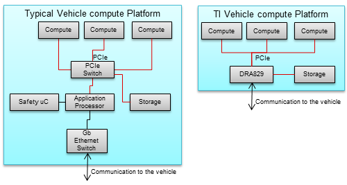
There are functional safety requirements for a portion of the functions. The DRA829 leverages more than 20 years of functional safety experience to support mixed criticality processing. Lockstep Arm® Cortex™-R5Fs enable ASIL- D while the entire SOC is ASIL-B capable. Extensive on chip firewalls enable the freedom from interference required to manage mixed criticality safety and non-safety functions simultaneously. Figure 2 compares a typical vehicle compute platform with one using the DRA829V. The DRA829V requires half as many packages saving cost, power and physical size.


Figure 2: Two examples of vehicle compute gateway systems

Automotive vehicle architectures are evolving to meet the demands of the industry trends. There is emerging vehicle architecture to enable the software defined vehicle based on a SOA, which means one to three vehicle compute platforms are needed per vehicle. TI’s new DRA82x family of processors was purpose-built for these requirements and help automakers and Tier-1 suppliers efficiently develop vehicle compute platforms that meet system needs and system cost constraints.

Make desktop 3D printing more affordable with DLP® Pico™ technology

$
0
0
3D printing has the power to bring imagination to life by giving it a concrete shape. A student can translate his understanding of the physical world into 3D objects. A designer can transform ideas into real objects that they can touch and feel before...(read more)

Testing TI BAW resonator technology in mechanical shock and vibration environments

$
0
0

Wouldn’t it be nice to know the condition of parts in your car exposed to mechanical vibrations or shock from the engine, or to get information about the status of systems operating under severe mechanical vibration conditions in an automated factory? With this information, you could perform predictive maintenance and replace fatigued parts before they fail completely, substantially reducing car problems or factory downtime. Check out this video demo of our crystal-less wireless TI BAW technology being put to the test and learn more in the technical article below.

(Please visit the site to view this video)


How BAW technology resists mechanical shock and vibration


Two important parameters for measuring vibration and shock are the acceleration force and vibration frequency applied to IoT-connected devices. You’ll find sources of vibration anywhere: inside a moving vehicle, a cooling fan in equipment or even a handheld wireless device. It is important that clock solutions provide a stable clock with strong resistance against acceleration forces, vibration and shock, as this assures stability throughout product life cycles under process and temperature variations.


Vibrations and mechanical shock affect resonators by inducing noise and frequency drift, degrading system performance over time. In reference oscillators, vibration and shock are common causes of elevated phase noise and jitter, frequency shifts and spikes, or even physical damage to the resonator and its package. Generally, external disturbances can couple into the microresonator through the package and degrade overall clocking performance.


One of the most critical performance metrics for any wireless device is to maintain a link between the transmitter and receiver and prevent data loss. Without the need for a crystal, BAW technology provides significant performance benefits for IoT products operating in harsh environments. Because BAW technology ensures stable data transmission, data syncing over wired and wireless signals is more precise and makes continuous transmission possible, which means that data can be processed quickly and seamlessly to maximize efficiency.


Evaluating BAW technology with high industry standards


TI has tested the CC2652RB thoroughly against relevant military standards because many MCUs operate in environments susceptible to shock and vibration, such as factories and automotive vehicles. Military standard (MIL)-STD-883H, Method 2002 is designed to test the survivability of quartz crystal oscillators. This standard subjects semiconductor devices to moderate or severe mechanical shock (with an acceleration peak of 1500 g) caused by sudden forces or abrupt changes in motion from rough handling, transportation or field operation. Shocks of this type could disturb operating characteristics or cause damage similar to what could result from excessive vibration, particularly if the shock pulses are repetitive.


Figure 1 shows a mechanical shock test setup for MIL-STD-883H, while Figure 2 shows the frequency variation of the CC2652RB compared to an external crystal solution. You can see that the maximum frequency deviation is about 2 ppm, while the external crystal solution is about 7 ppm at 2,440 GHz.


Figure 1: Mechanical shock test setup and test setup block diagram


Figure 2: Comparing the maximum radio (2,440 GHz) frequency deviation (parts per million) induced by mechanical shock on both BAW and crystal devices


Conclusion


BAW technology represents real progress within the evolution of IoT by reducing the amount of space required in some critical devices, like those in the medical field, and enabling the use of IoT in places characterized by frequent shocks or vibrations. BAW technology will be one of the catalysts in the connected world of the future across a vast array of sectors.

Resources

    • SimpleLink CC13x2 and CC26x2 software development kit

Customizing on-chip peripherals defies conventional logic

$
0
0
It is a familiar scene in labs across the globe: A design engineer is pushing the envelope, seeking to enhance functionality or improve performance. Unfortunately, while digging deep into low-level system timing, a design stalemate occurs. The potential...(read more)

Protect outdoor cameras from extreme weather with a temperature switch

$
0
0
Because of their role in security applications, it’s important that outdoor cameras do not malfunction or fail, regardless of whether they’re placed in tropical or frigid climates, or climates that experience both extremes in a given day....(read more)

Always make the right turn: how to design fault circuits in automotive lighting systems

$
0
0

It's incredibly important to indicate a system failure to users, especially when it comes to automotive lighting.

Consider the turn indicator in an automotive rear light, for example, which signals that a driver wants to change lanes or make a turn. A common and growing light source for turn indicators is LEDs, driven by a dual-stage LED driver circuit topology that includes a first-stage buck voltage regulator and a second-stage constant-current linear LED driver. Dual-stage topologies offer the advantage of thermal efficiency.

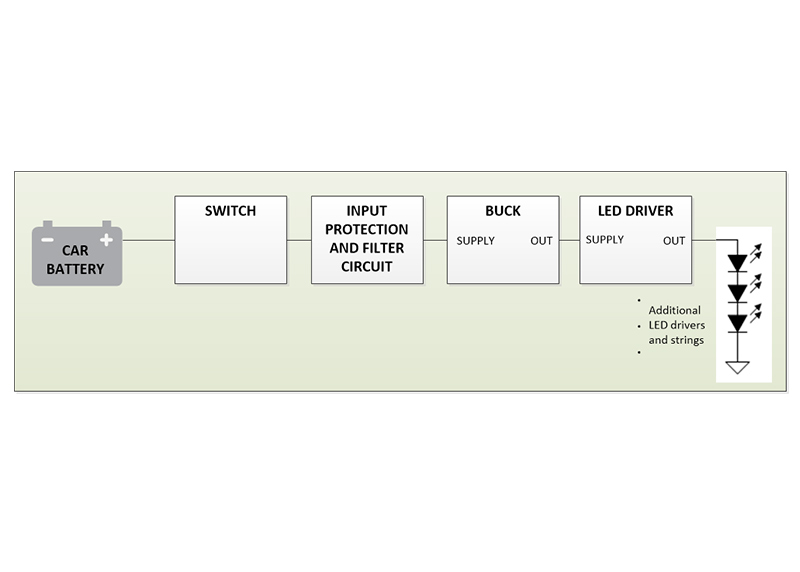
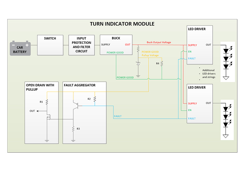
The LED-based turn indicator module shown in Figure 1 comprises a typical automotive battery, switch, input filter, buck regulator and some LED drivers. So what happens if the light stops working? How will you know? Which part of the system failed?

 Figure 1: Turn indicator moduleFigure 1: Turn indicator module

Buck regulator and LED driver integrated circuits implement diagnostic features in order to detect an event against faults. For example, the POWER GOOD signal is a diagnostic feature used to indicate whether or not the output of a buck is in regulation. Similarly, constant-current LED drivers output a FAULT signal to indicate LED short and open circuits.

In this article, I will focus on rear lighting fault circuits and how to combine PWRGD signals from a buck regulator and the FAULT signal from a LED driver to design a fault circuit.

The buck converter PWRGD signal

The POWER GOOD pin is typically an open-drain output with an external pullup resistor. The output asserts high in normal operation and low if the output voltage is low because of an incorrect output voltage, thermal shutdown or enable shutdown. For TI devices, check out buck regulators with POWER GOOD pin functionality.

According to data sheets, the POWER GOOD pin must be pulled high using recommended values. Given system requirements, it is possible to pull the POWERGOOD pin high to the output of a buck regulator using a pullup resistor. However, if the buck regulator output voltage is greater than the recommended pullup voltage, it’s best to use a Zener diode to clamp to a lower voltage.


Accelerate the evolution of passenger comfort and convenience

 Automotive lighting from front to rearExplore TI's design resources for automotive lighting.

LED driver FAULT signal

In TI linear LED drivers, the FAULT pin is an open-drain transistor with a weak internal pullup and must be pulled high in order to release the fault signal. In normal operation, the FAULT pin asserts high. If an LED short or open fault occurs, the device has an internal pulldown current and the FAULT pin asserts low.

TI’s automotive-grade LED drivers have two FAULT pin design options:

  • One-fail-all-fail (OFAF): Shuts down all devices and reports a fault if there is a fault in one of the devices.
  • Disabled OFAF: When one device has a fault, the remaining devices continue operating and a fault is reported.

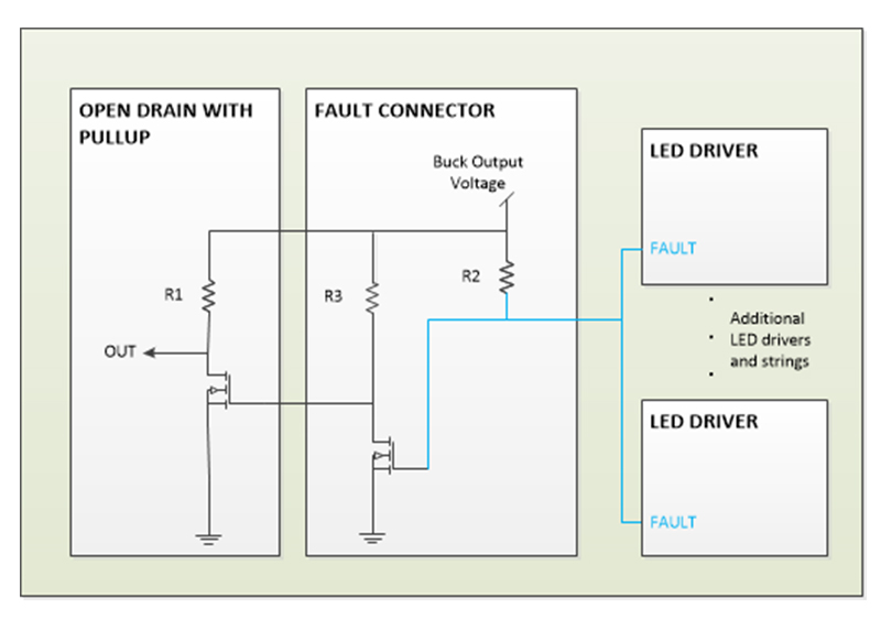
When connecting the FAULT pins of up to 15 devices together, the system uses OFAF. Figure 2 shows the fault connector circuit connected to the FAULT pins of LED drivers. The fault connector circuit is used to improve FAULT signal robustness. The open drain with pullup is used for easy interface with external circuitry.

Figure 2: Fault connector

Figure 2: Fault connector 

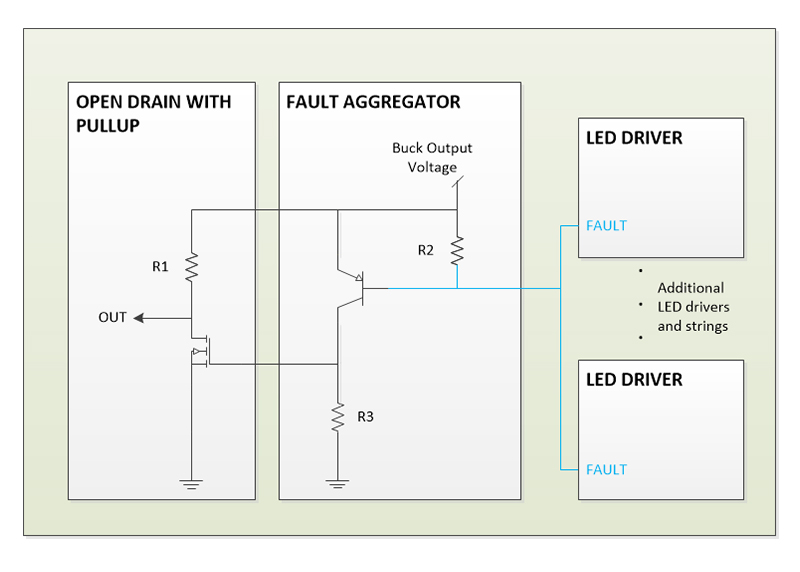
Disabled OFAF requires a fault aggregator circuit. Figure 3 shows the fault aggregator circuit connected to the FAULT pins of LED drivers. The open-drain output with pullup is used to assert OUT low in the event of a fault and high if there is no fault.

Figure 3: Fault aggregator

Figure 3: Fault aggregator

The fault aggregator circuit is defined as a fault pin pullup circuit. In order to disable OFAF, the FAULT pin must be pulled up to maintain a voltage greater than 2 V at all times. The P-channel transistor (PNP) is used to convert the FAULT pin from a current-controlled pin to a voltage. Pullup resistor R2 keeps FAULT greater than 2 V. Typically, a fault signal asserts low in the event of a fault and asserts high if there is no fault. Thus, the open-drain output with pullup inverts the logic of the fault aggregator circuit to assert OUT low in the event of a fault and high if there is no fault. You can omit the open-drain output with pullup from the design if the system requires OUT high in the event of a fault and low if there is no fault.

When a fault is triggered, the LED driver internally pulls down current, and the pulldown current flows through pullup resistor R2. The PNP turns on, the output of PNP goes high and OUT becomes low. When no fault is triggered, the LED driver internally pulls up and PNP acts as an open switch. The output of PNP goes low and OUT becomes high. In both cases, FAULT remains greater than 2 V.

Considering the turn indicator module, the buck regulator output voltage should power the fault aggregator circuit; a Zener diode can clamp the buck regulator output to a lower voltage. In case of a buck regulator failure, there is no power to the fault aggregator, and a fault is indicated.

The “Automotive high side dimming rear light reference design” shows how to design a fault aggregator circuit using TI’s TPS92630-Q1 and TPS92638-Q1.

Using POWER GOOD signal to enable an LED driver

One approach to combine the buck regulator POWER GOOD signal and LED driver FAULT signal is to take advantage of the enable (EN) pin of the LED driver. When the EN pin is high, the LED driver operates normally. When the EN pin is low, the LED driver is in sleep mode, with ultra-low quiescent current.

Figure 4 shows how to connect the POWER GOOD pin to the EN pin using pullup resistor R4 and a Zener diode. The Zener diode provides a lower pullup voltage for the POWER GOOD pin. The POWER GOOD pin is pulled high by R4 to the clamping voltage from the Zener diode.

Figure 4: Connecting POWER GOOD and EN

Figure 4: Connecting POWER GOOD and EN

By connecting the output of the POWER GOOD pin to the EN pin of the LED drivers, the POWER GOOD signal now controls the LED drivers. In normal operation, the POWER GOOD pin asserts high and the LED drivers are enabled. In the case of a buck regulator failure, the POWER GOOD pin l asserts low, the LED drivers are not enabled, the fault aggregator circuit has no power, and OUT becomes low – indicating a fault.

System fault analysis

The goal for a fault circuit is to indicate any fault in the turn indicator module that prevents the LEDs from turning on. The sources of a fault could be an incorrect voltage output from the buck regulator, incorrect current output from LED drivers or faulty LEDs.

Figure 5 shows the complete turn indicator module block diagram, where the POWER GOOD pin connects to the EN pin of the LED drivers using pullup resistor R4 and a Zener diode. The fault aggregator circuit disables OFAF.

Figure 5: Disabling OFAF with a Zener diode and fault aggregator

Figure 5: Disabling OFAF with a Zener diode and fault aggregator

When the system operates normally, the battery voltage is filtered and bucked down to power the LED drivers. The POWER GOOD pin is pulled up to the Zener diode clamping voltage, asserts high and enables the LED drivers. The LEDs then power on, with no short or open LED fault detected. Thus, FAULT asserts low, the fault aggregator asserts low, and no fault is indicated to the output.

Now consider a buck regulator output voltage fault. The buck output voltage is out of nominal range, and the POWER GOOD pin asserts low. The LED drivers are disabled and the LEDs are powered off. FAULT asserts low when the LED drivers are disabled. The fault aggregator has no power from the Zener diode clamp voltage, and the output goes low, indicating a fault.

The turn indicator module can fail in other ways. Some examples include an LED short or open circuit or LED driver thermal shutdown. The circuit shown in Figure 4 enables detection of these different fault types in the turn indicator module.

Conclusion

Automotive lighting systems are implementing more fault circuits. To save space and reduce cost for fault circuits, try connecting the POWER GOOD pin to the EN pin of the LED driver. For LED faults, consider using or disabling OFAF. Choose the design option that meets the requirements for your specific application.


What is an op amp?

$
0
0

Many textbooks and reference guides define operational amplifiers (op amps) as special integrated circuits (ICs) that perform various functions or operations, such as amplification, addition and subtraction. While I agree with this definition, it’s also important to note the importance of the voltages at the input pins of the device.

When the input voltages are equal, the op amp is usually operating linearly, and it is during linear operation that the op amp accurately performs the aforementioned functions. However, an op amp can change only one thing to make the input voltages equal: the output voltage. Therefore, the output of an op amp circuit is typically connected in some manner to the input, which is commonly referred to as voltage feedback.

In this article, I will explain the basic operation of a general-purpose, voltage-feedback op amp and refer you to other content where you can learn more.


Designing with op amps

 Explore TI Precision Labs, our on-demand training for analog engineers.

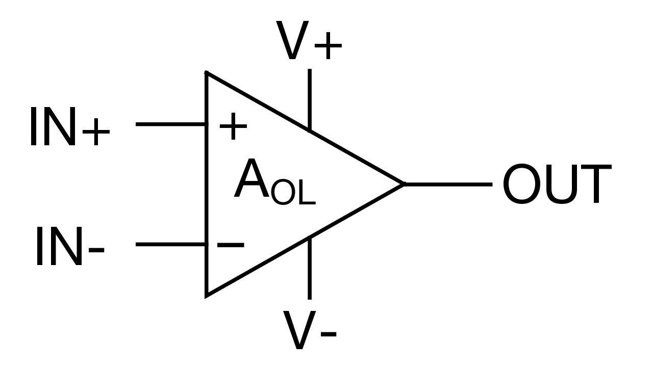
Figure 1 depicts the standard schematic symbol for an op amp. There are two input terminals (IN+, IN-), one output terminal (OUT) and two power-supply terminals (V+, V-). The names for the terminals may vary from manufacturer to manufacturer or even within a single manufacturer, but they’re the same five terminals nonetheless.

For example, you may see Vcc or Vdd instead of V+. Similarly, you may see Vee or Vss instead of V-. Other labels for the power-supply terminals will differ because they refer to the types of transistors inside the device. For example, when using bipolar junction transistors (BJTs) inside of op amps, the power supplies correspond to the collector and emitter terminals of the BJTs: Vcc and Vee. When using field-effect transistors (FETs) inside op amps, the power-supply labels correspond to the drain and source of the FETs: Vdd and Vss. Today, many op amps contain both BJTs and FETs, so V+ and V- are common labels, regardless of the transistors inside the device. In short, don’t get caught up on the pin labels; just understand what they do.

Figure 1: General-purpose op-amp schematic symbol

Equation 1 expresses the transfer function of an op amp:

      (1)

In Equation 1, AOL is known as the “open-loop gain,” and it is generally an extremely large value in modern op amps (120 dB, or 1,000,000 V/V). As an example, if the voltage difference between IN+ and IN- is just 1 mV, the op amp will try to output 1,000 V! In this configuration, the op amp is not operating in a linear region because the output is not able to make the inputs equal to one another (remember, ideally IN+ equals IN-). Therefore, op amps need a way to control the open-loop gain, which is done with negative feedback.

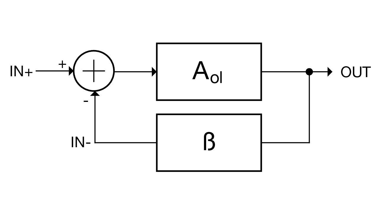
Figure 2 depicts an op amp as part of a feedback control system. You will notice that the output, OUT, is fed back to the negative input, IN-, through a block labeled ß. ß is known as the feedback factor, and generally uses resistors to divide down the output voltage.

Figure 2: Op amp with negative feedback

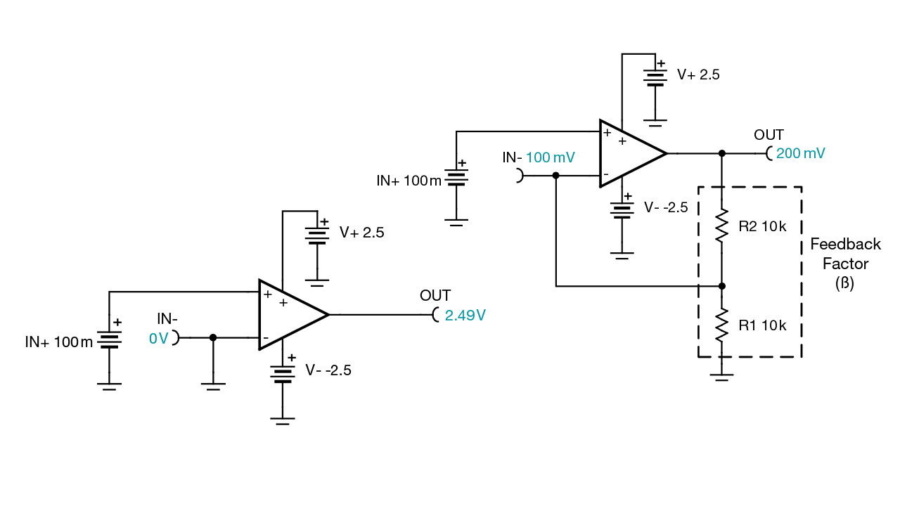
Figure 3 compares an op amp operating in open loop versus one with negative feedback. These TINA-TI™ software simulations use a nearly ideal op amp with power supplies in order to limit the output voltage. Notice that for the open-loop configuration on the left, the output is nearly equal to the positive power supply (V+). This is because there is a small difference (100 mV) between the input pins. This small voltage is amplified by the open loop gain, which forces the output to one of the supply voltages. In the negative feedback or closed-loop version on the right side of Figure 3, the voltage divider on the output of the op amp necessitates an output voltage of 200 mV in order to make the inverting and noninverting inputs equal.
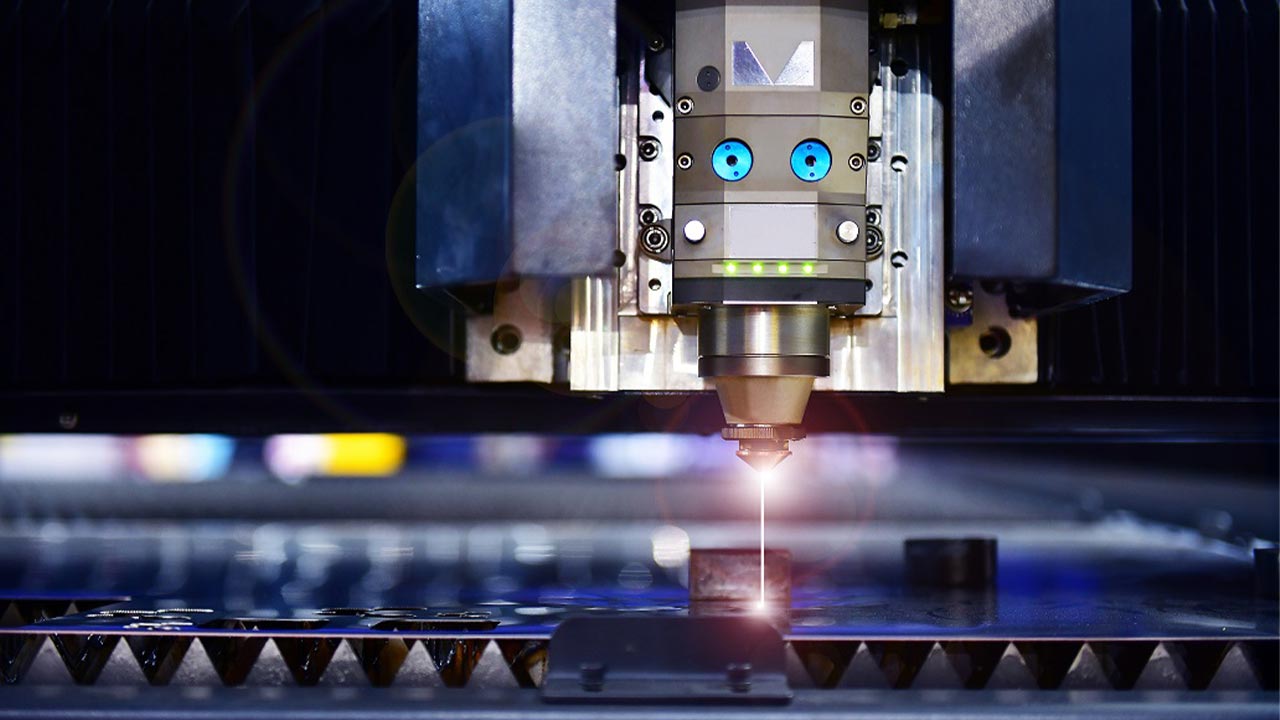
Figure 3: Open loop (left) versus negative feedback (right)

The amplification of the input voltage is known as gain. It is a function of the resistor values in the feedback loop. Equation 2 depicts the gain equation for the circuit on the right in Figure 3, which is known as a noninverting amplifier. You’ll see that the calculated output voltage corresponds to the simulation. If you’re interested in learning more about this circuit (and other common op-amp circuits like the buffer, inverting amplifier and difference amplifier), you can download the e-book, the “Analog Engineer’s Circuit Cookbook: Amplifiers.”

      (2)

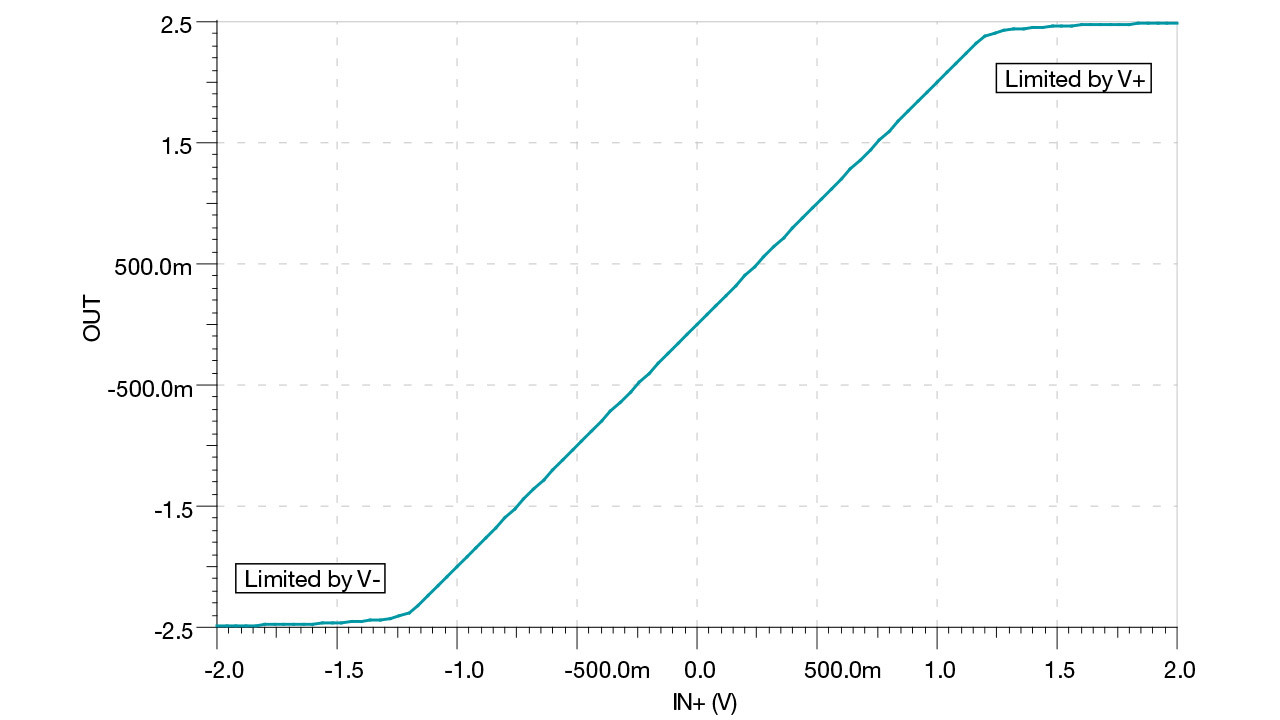
The output of an op amp is limited by the supply voltages. Figure 4 is a plot of the output voltage versus the input voltage of the noninverting amplifier in Figure 3. Notice the limitation where the output saturates as it approaches the positive and negative supplies.
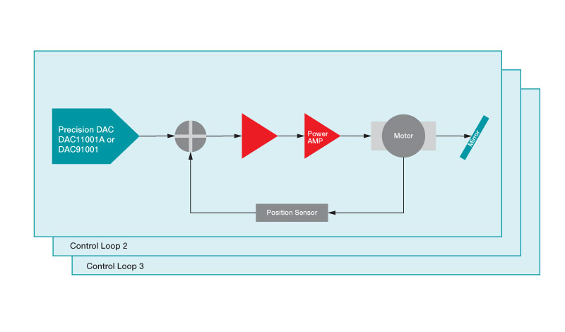
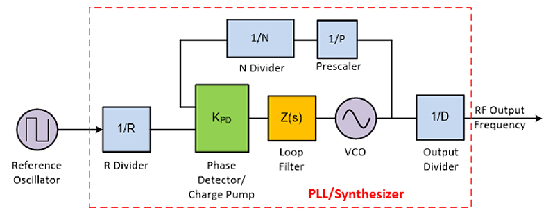
Figure 4: Output versus input voltage for a noninverting amplifier circuit

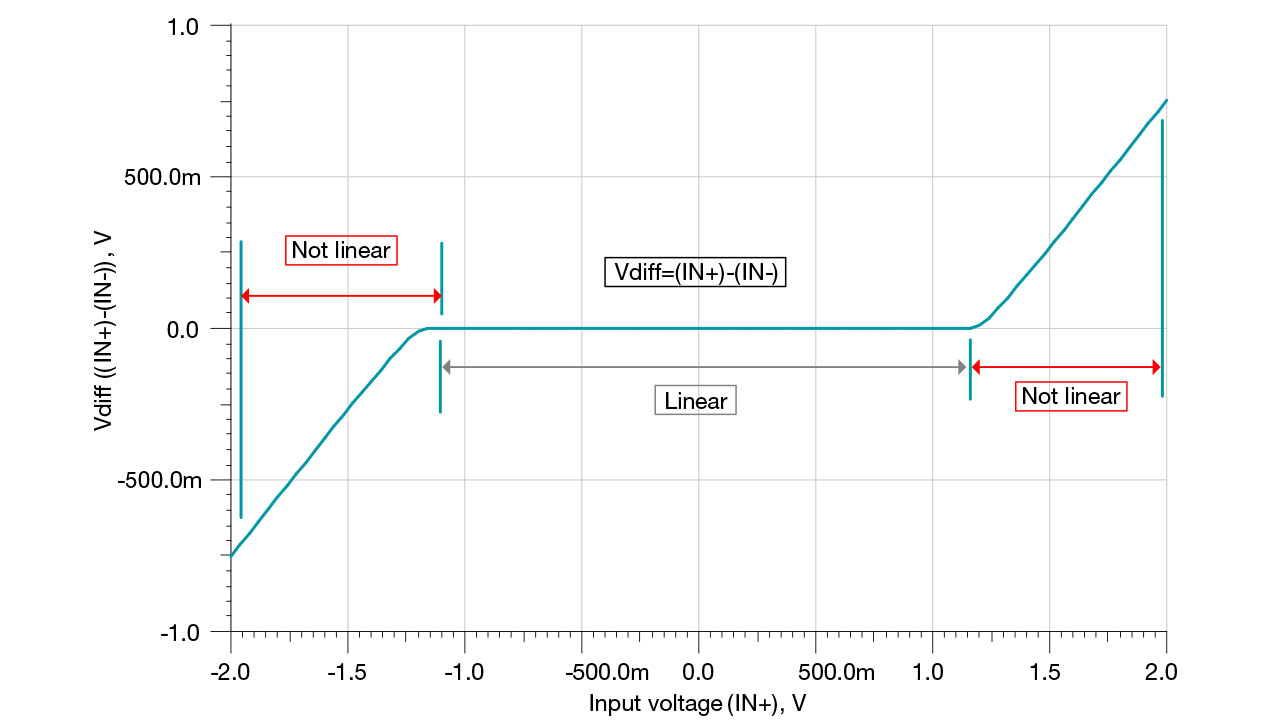
Due to this limitation, you’ll see in Figure 5 that the voltage difference between the input pins, Vdiff, increases as the output approaches the supplies. It is only when the inputs are nearly equal that the op amp is operating in a linear region.

Figure 5: Vdiff versus IN+ for a noninverting amplifier circuit

In order to understand op amps at a deeper level, check out our analog curriculum, TI Precision Labs. This curriculum delves further inside the op amp and discusses fundamental nonidealities such as input offset voltage (Vos), input bias current (IB) and input/output limitations. There are also lectures on advanced topics such as op amp bandwidth (BW), slew rate (SR), noise, common-mode rejection ratio (CMRR), power supply rejection ratio (PSRR) and stability. In addition to lectures, some of the topics have hands-on lab experiments. In order to conduct these experiments, you’ll need the corresponding op-amp evaluation module.

If you’re more of a tinkerer at heart, you may be interested in the Universal Do-It-Yourself (DIY) Amplifier Circuit Evaluation Module (for single-channel devices), the Dual Channel Universal Do-It-Yourself (DIY) Amplifier Circuit Evaluation (for dual-channel devices) or the DIP Adapter Evaluation Module (which can be used in conjunction with a standard prototyping board or breadboard). The DIY EVMs support a variety of packages and have a number of standard op-amp circuits, such as the noninverting amplifier described in this article, inverting amplifier, buffer and filters (both Sallen-Key and multiple feedback). Because the dual in-line package (DIP) adapter EVM converts many standard surface-mount packages to DIP for use in conjunction with a breadboard, you can evaluate just about any amplifier in just about any configuration.

So that’s the fundamental principle of an op amp: it is only linear when the voltages at the input pins are equal. In order to achieve this, however, an op amp can only adjust its output voltage. Output swing limitations can cause the input voltages to diverge from one another, which yields nonlinear, undesirable behavior.

Additional resources

7 signs you might be a power-supply designer

$
0
0

For aspiring electrical engineering students trying to decide what to specialize in, I strongly encourage considering power electronics. Every new electrical or electronic product needs a power supply – talk about job security! Despite what you might think, the field is full of challenging work and opportunity for innovation, driven by the quest for smaller devices and higher efficiency.

It may not be as sexy as being a digital designer. But if you decide to take the path less traveled, you’ll be rewarded with challenging and innovative work, and eventually find yourself in a tightknit community of digital outcasts.

Power-supply designers are a different breed. Yet there are common threads that weave through the fabric of the power community and bind us together.

You might be a power-supply designer if ...

1. … you brag about your low IQ. Forrest Gump taught us that a low IQ isn’t necessarily a bad thing. Of course, in power supplies, IQ refers to quiescent current – not intelligence quotient – and it can draw some strange looks from anyone eavesdropping on a conversation. Power-supply designers are always trying to reduce their IQ in order to extend battery life and improve efficiency. This is particularly important with low-dropout (LDO) linear regulators. At TI, we are proud of our portfolio of low-IQ LDOs, which enable designers to prolong battery life and performance in their systems.

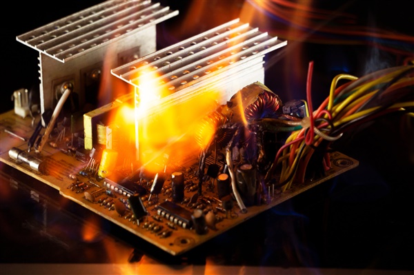
 2. … you keep retelling the same story involving an exploding capacitor. We’ve all been there. Whether it was due to soldering the capacitor into the circuit backwards, an overvoltage condition or too much ripple current, nothing will draw a crowd to your lab bench faster than an explosion (Figure 1).


Figure 1: Blame it on the technician!

After your pulse rate goes back to normal and the cloud of magic smoke clears from the lab, it’s natural to admire the awesomeness of what just transpired. Don’t be ashamed to share vivid details of your impromptu fireworks show with your peers. We won’t judge, and will happily reveal tales of calamities past. Always use your protective eyewear, people!

3. … you’ve ever searched Wikipedia for the truth table of a simple logic gate. If you don’t use it, you lose it. After working in the analog world of power-supply design for over 20 years, I have lost touch with the realm of 1s and 0s. Whenever I struggle with a digital circuit, I pull out Figure 2, which I found in a fortune cookie many years ago. It calms my nerves and allows me to focus on the problem.


Figure 2: The most perfect fortune cookie fortune ever

Digital control of power supplies is more common now than when I began my career. If you need help with designing a digital power supply and don’t have a fortune of your own, TI offers a plethora of digital power products and resources that offer flexibility, efficiency and integration so that you can meet your dynamic system needs and reduce your total cost.

4. … you’ve ever had to explain that perpetual motion is impossible. If you design power supplies long enough, at some point you’ll be asked to create a power supply that delivers more output power than what’s available from the input source. It’s amazing how difficult it is to convince some people that this violates the first law of thermodynamics (energy is neither created nor destroyed). The next time you are faced with this dilemma and want to be bold, you could simply ask rhetorically, “So, you want this power supply to be 110% efficient?” And if that doesn’t work, try asking them what is wrong with Figure 3.


Figure 3: Infinite power

Of course, the most sensible response is to renegotiate the power requirements of the input, the output or both – and then design with TI’s highly efficient DC/DC switching regulators to deliver the most power possible from a limited power source.

5. … you’ve ever told management that they can only meet two out of three goals. The old saying “two out of three ain’t bad” definitely applies to power-supply design. Of course, I’m referring to the three trade-offs of cost, size and efficiency, which unfortunately, your manager or customer may not fully grasp.

You can make a power supply smaller and cheaper by switching at a higher frequency, but that will make it less efficient. You could keep it small and make it more efficient by using better components, but that makes it more expensive. Or you could make it more efficient and cheaper by using larger components. Sorry, but just like everything else in engineering, nothing comes for free. Good luck explaining this to your manager!

 6. … you speak in a language only other power-supply designers understand. Like siblings who have spent way too much time with one another, over time, power-supply designers tend to develop new words to communicate among themselves. To the outsider, this will sound like nonsense, but to the power-supply designer these are highly technical terms.

Many years ago, one of my great mentors documented these terms so others could understand our conversations. I wish I could share this glossary of power-supply terms publicly, but not all are appropriate to publish.

7. … you count the days until the next Power Supply Design Seminar (PSDS). The PSDS has been the premier industry-led seminar for practical power-supply design since the 1980s. Every two years, we hit the road to bring training directly to you, with new content that has been carefully screened to be useful, educational and interesting.

Whether you’re new to power-supply design or have been designing switching power supplies for decades, the PSDS has something for everyone. It provides a chance to learn something new, get a refresher of the basics, and connect with others in the power-supply community in your local region.

Over the decades, Unitrode and TI have created a treasure trove of reference material for power-supply design, all of which is free to access. The show continues with the 2020 PSDS beginning soon – you can register here.

If you’re new to the power-supply community, welcome to the secret society of power-supply designers! If you already identify as one of us, please share your stories and other signs that “you might be a power supply designer if …” by commenting beneath this article.

For all of you, I look forward to connecting at the 2020 Power Supply Design Seminar.

How intelligent, automated robots on wheels are changing last-mile delivery

$
0
0

Early last year, students at George Mason University were joined by 25 somewhat unusual, new residents. Measuring just under 2 feet tall, Starship Technologies' fleet of boxy wheeled robots were on campus to deliver anything from coffee to sushi.

English major Kendal Denny immediately placed an order through Starship's app, which is paired with the university's meal plan.

“They were this new technology that no one on campus had ever experienced before," she said.

George Mason's executive director of campus retail operations, Mark Kraner, had been struggling with competition from other food delivery services – but managing the university's own human delivery force didn't seem viable.

“It's difficult to make sure you have the right number of people in the right places at the right times,” he said.

Rolling around at 4 mph, typically delivering orders within 15-30 minutes, Starship’s robots have quickly adapted to the campus, and the students have adapted to them, too.


 Read our white paper: How sensor data is powering AI in robotics.

“I used it a lot during exam periods when you don't have time to go to the dining hall and stand in the line," said recent graduate Sofya Vetrova. “It's much easier to just order from your phone. You get notified when the delivery is downstairs, so it’s very convenient and less time-consuming."

Tens of thousands of food orders have been delivered so far across campuses nationwide, including at The University of Texas at Dallas. At George Mason, Mark is looking into expanding the service to deliver mail, groceries and bookstore orders.

"Cars are really difficult on campus because parking spaces are rare," he said. “But the robots don't need them, and they can weave easily around students, so they're just like anyone else walking along a sidewalk."

The challenge of the last mile

For George Mason students, the robots simply represent convenient food delivery, but automated delivery could mean much more on a global scale.

According to the Logistics Research Centre of Heriot‐Watt University, the last mile -- the final stage of delivery from a transportation hub to the customer's home -- contributes an average of 181 grams of CO2 into the air per delivery.1  And, with the majority of deliveries taking place in highly populated urban areas, congestion is a major concern. A combination of increasing urbanization alongside the growth of e-commerce is only increasing the problem, as urban freight looks set to increase by 40% by 2050.2

“The last mile of delivery is responsible for many of the problems we see with trucks polluting the air and blocking traffic lanes," said Matt Chevrier, a robotics expert with our company. "If we could replace these with smaller robots, which contribute significantly less pollution to the streets and can insert themselves into ordinary traffic, it could have a significant impact on urban air quality and on urban quality of life in general."


Robots in the wild

Unlocking the potential of automated delivery is not without its challenges. The first wave of robotics unfolded in factories and laboratories, taking the form of fixed robotic arms that precisely repeat pre-programmed routines, safely inside fenced-off zones.

As robots are being released into the real world, and expected to successfully navigate both the diverse obstacles presented by the urban environment and the unpredictable behaviors of their human co-inhabitants, then they need to independently perceive, understand and learn from their surroundings.

Fundamentally, that requires a few things: precise, accurate sensors, fast connection systems analogous to the human nervous system, rapid data processing -- often enabled by artificial intelligence – and quick reactions. Starship seems to be achieving all of these feats.

Multiple sensing technologies are used by robots depending on their size and speed. Some use LIDAR, ultrasonic, cameras, radar or a combination of these technologies. LIDAR is often used for autonomous vehicles with high speeds requiring long breaking distances. Starship doesn’t use LIDAR and relies on other sensor fusion for navigation and obstacle detection.

Our company’s TI mmWave sensors operate at a wavelength smaller than typical radio waves, but greater than lasers. This allows the sensor to see in challenging environmental conditions – such as darkness, extreme bright light, dust, rain, snow and extreme temperatures.

TI mmWave sensors also enable accurate detection of transparent objects, such as glass. “TI mmWave brings a lot of advantages new opportunities by ensuring that if something needs to be detected, it can reliably be detected," Matt said.

Intelligent Robots

Detection is only half the story, however. Wheeled robots also need to identify what's in front of them and then judge how best to respond. In dynamic environments, it isn't feasible to await a decision while the raw data is sent to the cloud for processing, which means the machine learning algorithms need to run on the robot itself.

Our company's Sitara™ processors are specifically optimized for the low-power operation of machine learning in the robot itself, enabling mmWave sensor data to be utilized for accurate categorization in real time. For the longer term, this data can also be uploaded to stationary computer systems, where time-constraints and power demands aren't an issue, and used to further train identification algorithms, while also building up a detailed map of the robot's typical routes.

“We've all had situations where the GPS fails on us, or doesn't give us an accurate enough location," Matt said. “Supplementing this with the robot's own map can make navigation much more reliable."

Back at George Mason, the robots have been quickly accepted as part of the student community. “People like to take pictures with them and just watch them, because they are cute," Kendal Denny said. “They're kind of our new mascot."

  1. Logistics Reearch Centre, Heriot-Watt University.
  2. Supply Chain Dive.

Choosing buck converters and LDOs for miniature industrial automation equipment: what to consider

$
0
0

As the factory automation and control equipment market evolves, shipments of equipment with sensors such asfield transmitters, machine vision and position sensors are increasing. As a result, the demand for feature-rich power integrated circuits (ICs) that could power these devices is also growing.

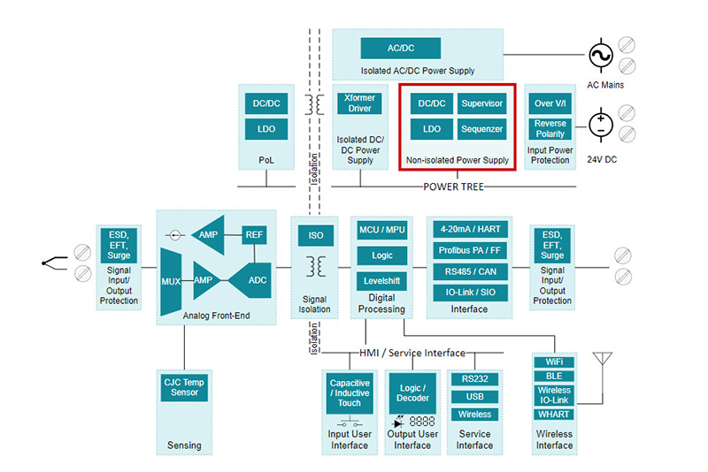
Figure 1 shows a block diagram of a temperature transmitter. The nonisolated power-supply subsystem (highlighted in red) consists of a low dropout regulator (LDO), a DC/DC converter or a power module. In an earlier technical article, “Powering tiny industrial automation control equipment with high-voltage modules: how to ensure reliability,” my colleague Akshay Mehta explained how to power miniature industrial automation control equipment with high-voltage modules. In this article, I’ll take a look at how to use buck converters and LDOs for the same purpose.


Figure 1: Temperature transmitter subsystem

High input voltage, higher stakes

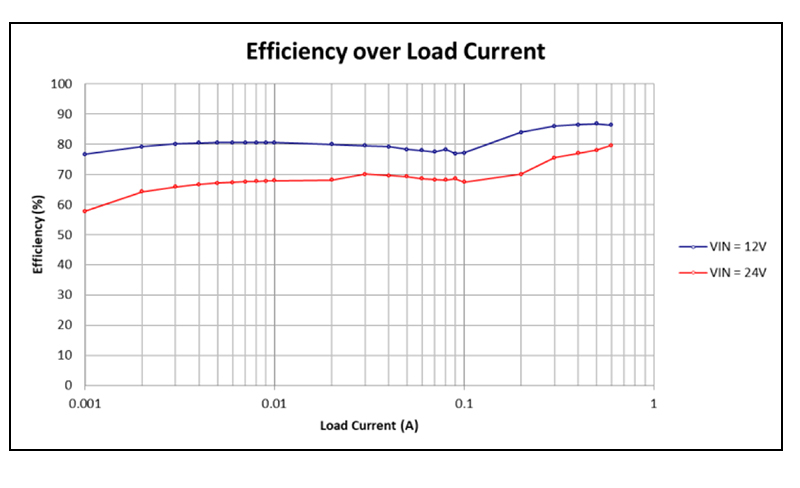
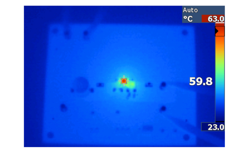
There are a number of ways to regulate the input DC voltage in factory automation and control equipment. You can use an LDO, a DC/DC converter or a power module. LDOs such as the TPS7A47 are commonly used in sensor power supplies due to their simple design and ability to attenuate input noise and deliver a ripple-free output voltage. DC/DC converters are a good choice for applications operating at lower output voltages, higher input voltages or higher output currents. For example, the LMR36503 and LMR36506 DC/DC converters enable a low shutdown current specification of 1 µA and an operating quiescent current specification of 7 µA. For loads with low output currents – less than 20 mA – these performance specifications ensure higher efficiency for 4- to 20-mA loop applications. Figure 2 shows the efficiency and thermal performance of the LMR36506 converter.


Figure 2: Efficiency and thermal performance at 24 VIN, 5 VOUT, 2.1 MHz at 0.6A
Big challenge, small solution
 
Most field sensors are small, which constrains the size of the printed circuit board (PCB). For instance, ultrasonic sensors with M12 housing need a PCB width less than 9 mm. Incorporating power-supply components on a small PCB in a subsystem – as shown in Figure 1 – becomes very challenging for hardware designers.
 
A power module with an integrated inductor such as the TPSM265R1 can address this challenge, since DC/DC converters require that you use additional components such as an inductor to maintain high frequencies. However, if you prefer to use a DC/DC converter, you can reduce the total solution size by choosing converters that operate at higher frequencies, which reduces the size of the inductor and capacitor, or by selecting a device with integrated external components.
 
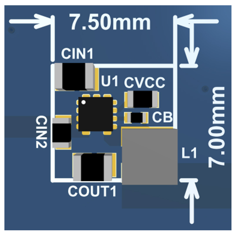
For example, the LMR36503 and LMR36506 come in 2-mm-by-2-mm packaging with as witching frequency enables you to use an ultra-small inductor and output capacitor, while the internal loop compensation and fixed 5-V/ 3.3-V output options reduce the overall external component count. It is possible to optimize the total solution size further, as shown in Figure 3.
 

Figure 3: LMR36506 example solution size
Lowering EMI, raising the standard
 
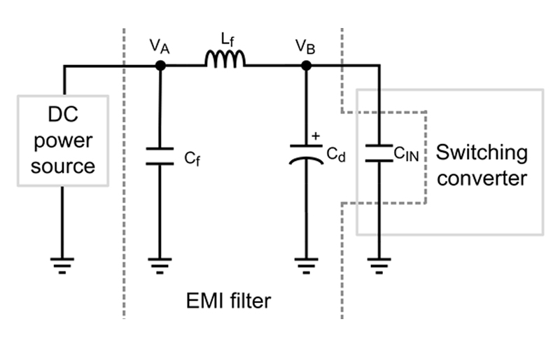
All switching power supplies generate electromagnetic interference (EMI) by virtue of the fact that they switch the input voltage using fast rise and fall times. An EMI filter and metal shielding can help resolve EMI issues, as Figure 4 illustrates. However, a multiple-stage EMI filter could reduce the efficiency of your application while increasing solution size and design costs. To combat this reduced efficiency, use DC/DC converters designed to provide lower EMI.

Figure 4: An EMI filter structure for DC/DC converters
 
The LMR36503 and LMR36506 are designed with a flip-chip on-lead (FCOL) technology, which eliminates power device wire bonds that might result in higher package parasitic inductance. As shown in Figure 5, the IC is flipped upside down, and copper posts on the IC are soldered directly to a patterned leadframe. This reengineered construction enables a small solution size and a low profile, as each pin attaches directly to the leadframe. In addition, the flip-chip package lowers package parasitic inductance versus traditional wire-bond packages, resulting in much lower ringing and noise generation during switching transitions.


Figure 5: Wire-bond quad flat no-lead and FCOL packages
Conclusion
 
As the field sensor housing gets smaller, the constraint on PCB size becomes more of a challenge for board designers to provide power to the sensors. In this case, the LMR36506 is an option for meeting this challenge.
 
Additional Resources:

Protecting your power amplifier stage with analog switches

$
0
0

As the story of “The Hare and the Tortoise” taught us, sometimes it pays to be steady and calculated. With growing demand from consumers for higher bandwidth and speeds for their wireless data, the pressure is on semiconductor manufacturers to design systems that meet these requirements – much like how the hare focuses on being the fastest to reach the finish line. However, as the tortoise shows, it is just as important to be steady in this pursuit by ensuring that systems are rugged and reliable.

Because communications equipment, such as radio units and active antennas, is primarily based outdoors, it’s critical that internal components operate reliably regardless of environmental factors. Analogous to Aesop’s fable, systems must be high performing (like the hare), while being rugged (like the shell of the tortoise) to protect internal circuitry from external fault conditions. One way to ensure protection is to use an analog multiplexer, also known as a “mux,” to protect the internal power amplifier (PA) stage.

Why the PA stage?

Amplifier integrated circuits (ICs) use electric power from a power supply to increase the power of an input signal. By using an amplifier, you can produce a strong output signal from a weak input signal. For example, PAs are used to drive the loads of output devices, such as headphones, speakers, servos and radio frequency (RF) transmitters.

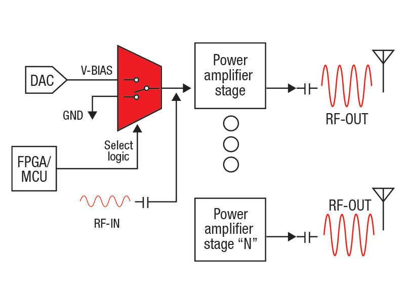
In the case of RF transmitters, RF PAs amplify low-level RF signals in massive multiple-input multiple-output (MIMO) antenna systems. Traditional massive MIMOs contain eight transmitter and eight receiver (8T8R) RF channels to amplify their antenna signal. In contrast, modern 5G systems will have up to 64T64R channels that increase download/upload data rates and throughput. Having this many channels in one remote radio unit requires protecting each channel from external fault conditions. A simple and cost-effective way to protect a system from these fault conditions is to use a 2-to-1 analog switch per channel, as shown in Figure 1.

PA stage protection per channel using an analog switchAs you can see from Figure 1, there are multiple PA stages based on the number of transmit and receive channels in the radio unit. Getting these PAs to function correctly requires applying a bias voltage (V-BIAS) to the gate of each FET. Unfortunately, V-BIAS is susceptible to external fault conditions such as overcurrent, overvoltage or overtemperature events that can exceed nominal safe values. In such cases, a field-programmable gate array or microcontroller detects the fault condition and immediately sends a select logic signal to the mux, disconnecting the V-BIAS signal path. Without the V-BIAS signal, the PA stage turns off, protecting the channel from the fault condition. Ultimately, the 2-to-1 analog switch turns the PA stage off in the event of a fault while providing a safe path to ground for the low-level RF signal (RF-IN). Analog switches, such as one-channel, 2:1 general-purpose analog multiplexers with 1.8-V logic control like the TMUX1219 or TMUX1247, can safely perform this function while operating at temperatures up to 125°C. Additionally, they can be directly controlled by 1.8-V field-programmable gate arrays or microcontrollers (MCUs) without the need for a level shifter due to their 1.8-V logic support. Read the application note, “Simplifying Design with 1.8 V logic Muxes and Switches” to learn more about the 1.8-V logic of these devices.

Protecting remote radio unit RF channels is critical because a fault event in one of these channels can significantly damage a system. With up to 64 channels per unit, this level of protection is critical to designing a high-bandwidth, high-speed system that has reliable performance. So if you keep the tortoise’s mindset when considering reliability and protection, you will remain in the race to meet the needs of next-generation networks.

How DACs can help you increase the precision of laser marking systems

$
0
0

Even when selling hundreds, thousands or even millions of products, many companies individually mark every single unit they sell with a brand or logo. The task of marking brands and etching logos is performed by laser marking machines, and the process requires a very high level of precision. As the technology progresses, designers of these systems are under pressure to make laser marking machines even more accurate so that more detailed markings are possible.

A laser marking machine (Figure 1) uses a high-intensity, low-power laser to etch a very precise design on anything from a cellphone to something like hand tools and printed circuit boards (PCBs). To create the desired output, the laser needs to be very carefully guided with the help of a precision digital-to-analog converter (DAC).

Figure 1: A laser cutting machine

So how does the DAC contribute to controlling the laser? The DAC is responsible for providing a very precise output voltage, which is then used as the analog input for a motor. Each specific analog input code from the DAC is related to a specific motor position. This motor is responsible for moving a mirror, which can be repositioned in the x, y or z planes to guide and reflect the laser and position it on the end equipment, where it can then alter the material’s surface and etch a logo, text or barcode. See Figure 2.

Diagram of DAC providing output for motor control of mirror

Figure 2: TI’s DAC11001A providing an output to the analog motor-control loop

As products that require etching become smaller, such as PCBs and some consumer goods, the precision of a laser marking system must increase. TI’s DAC11001A and DAC91001 offer 20-bit and 18-bit resolutions, respectively. These resolutions are important because they translate to the number of voltage steps available at the output of the DAC. An 18-bit resolution, for example, would have 262,144 unique codes (see Table 1), allowing for that many motor positions to control the laser. A 20-bit DAC offers 1,048,576 unique codes, providing far more granularity and far more precision.

16-bit = 216 = 65,536 (0 to 65,535)

18-bit = 218 = 262,144 (0 to 262,143)

20-bit = 220 = 1,048,576 (0 to 1,048,575)

Table 1: Calculations for DAC resolution to number of codes (16 to 20 bit)

What other benefits come with laser making systems utilizing 20-bit DAC performance? Well, if a full turn of the motor equates to 1 radian, what kind of step size do you need? Existing systems have a resolution of about 10 microradians for around 1 radian full-scale range. This equates to a resolution of 18 bits, ideally, but with system-level nonlinearity, many designers desire 20-bit resolution. This is where DAC11001A can help by offering nearly four times the number of output codes, and by extension, even finer control of the motor.

Another concern to consider is motor vibration. Any glitch in laser marking systems can adversely affect the final etching. These systems are very sensitive to residual motor vibration because the control loop has a multiple-order transfer function. Designers use complex techniques to achieve better performance, from selecting a low vibration motor to using complex control system logic. One of the key causes of motor vibration is the code-to-code glitch from the DAC. DAC11001A and DAC91001 have a very low code-to-code, code-independent glitch of 1nV-s. This is achieved through an integrated track-and-hold circuit that isolates the output of the DAC from the inherent code-to-code glitch of the internal resistor ladder.

As we have seen, laser marking machines have to contend with many variables with trying to achieve high precision. The DAC plays a pivotal role in solving this problem and can make a designer’s work much easier. Innovative solutions that offer higher resolution for increased accuracy and better glitch performance can make all the difference in laser marking designs.

Additional resources


Adjusting VOUT in USB Type-C™ and wireless charging applications, part 1

$
0
0

For applications using USB Type-C Power Delivery (PD) and wireless charging, the output voltage (VOUT) from the charger can fluctuate higher or lower than the input voltage. Four-switch buck-boost regulators are popular in these applications because adjusting their feedback signal can dynamically change the VOUT.

A buck-boost regulator’s output voltage can be adjusted either by varying the error amplifier’s reference voltage (VREF) or by varying the feedback voltage. If monolithic pulse-width modulation (PWM) four-switch buck-boost controllers such as TI’s LM34936 and LM5176 do not provide the ability to access VREF, however, varying the feedback voltage becomes the only way.

To help you design systems using buck-boost controllers with dynamic output voltages, in this series I will discuss a few options for using the feedback signal to adjust the output voltage. The first installment will focus on using switched resistors, while the second installment presents a different approach that requires fewer components and signal lines.

Understanding the VOUT setting and feedback signal

Figure 1 shows a typical VOUT setting for the controller and error amplifier. By looking up the VREF for the error amplifier in the data sheet, Equation 1 calculates VOUT by setting the values of R1 and R2:


Figure 1: Feedback circuit and VOUT setting

Using switched resistors to adjust VOUT

Figure 2 shows a simple option to dynamically adjust VOUT between two voltage levels by incorporating a switch, S1. Assume that S1 is an ideal switch, and that its impedance is infinity when off and 0 Ω when on. When switch S1 is turned off, R3 is not in the picture of the VOUT setting, and is simply the same as given in Equation 1. To avoid confusion in this discussion, let’s assume that the voltage is VOUT1, as expressed by Equation 2:

If S1 is turned on, it will place R3 in parallel with R1. The new output voltage, VOUT2, will satisfy Equation 3:

where

This results in VOUT2 being greater than VOUT1. By solving Equations 2 and 3, you can determine the resistor values. By toggling S1, you can switch VOUT between VOUT1 and VOUT2.


Figure 2: VOUT adjustment with a switched resistor

Preventing a false OVP trigger

Some PWM controllers like the LM34936 and LM5176 have built-in output overvoltage protection (OVP), implemented by monitoring the feedback (FB) pin voltage. If the FB pin sees >10% above VREF, the controller riggers OVP and stops switching until after the FB voltage falls below the hysteresis of the OVP threshold. Because of this feature, any abrupt resistor switching should be prevented, since turning off S1 suddenly will cause the FB voltage to jump up instantaneously and create a false OVP event. The solution is to switch S1 gradually, where R5 and C1 delay the on/off command of S1 to engage or disengage R3 gradually.

There are a couple of factors involved in selecting the resistor-capacitor (RC) delay time constant; the RC needs to match up with the loop response time, as well as the transition time between VOUT levels specified by the application, in order to enable proper transition between the two voltage outputs.

Multivoltage programming

Adding switched resistor branches can program additional VOUT levels. Figure 3 shows an approach employing three switched resistor branches to set the four VOUT levels for USB Type-C PD applications.


Figure 3: Three switched resistor branches for four VOUT settings

Table 1 summarizes the programming schemes for the four different voltages.


Table 1: Programming switched resistors for USB Type-C PD

As shown in Figure 4, it is important to make sure that switching to different resistors won’t trigger a false OVP event in the feedback loop. Incorporating an RC for each of the switches will help avoid an OVP event while switching to the proper voltage rail at the appropriate time.


Figure 4: Gradually switching the resistor to avoid triggering an OVP event during dynamic VOUT adjustment

Conclusion

By incorporating switches and resistors into the feedback loop, buck-boost converters can dynamically adjust the VOUT for USD Type-C PD and wireless charging applications. This approach is straightforward, simple and easy to implement. Controlling the speed of the switches is a requirement when using four-switch buck-boost controllers.

For a different approach using fewer components and signal lines, see the second installment of this series.

Additional resources

Why component integration carries weight for space-based PLL synthesizers

$
0
0

In space, no one can hear you scream about your overcomplicated and expensive satellite PLL synthesizer design.

Designing a phase-lock loop (PLL) synthesizer requires multiple individual components and discrete devices that take up a lot of volume and add significant mass. A typical PLL design might consist of a discrete voltage-controlled oscillator (VCO), a synthesizer and often an additional pre-scaler/divider or an output multiplier to accommodate higher frequencies. In some cases, even discrete phase detector/charge pumps are used to minimize noise in the system. With a long list of critical components, it’s not surprising that size and complexity would create challenges for designers working to create smaller, lighter systems that they intend to launch into space.

The challenge is similar to what mobile phone designers faced when implementing radio frequency (RF) and microwave components in early mobile devices. Relying on the integrated circuits (ICs) available at the time, these handheld devices required a plethora of discrete components – resulting in expensive, bulky devices with miniscule battery life.

Although the synthesizers in a mobile phone and a satellite system have largely different requirements, they do share the challenges for maintaining performance while reducing mass/volume. So, how did we get from brick-sized phones to the sleek and pocket-friendly smartphones today, and how can satellite system designers simplify their PLL designs? By integrating RF and synthesizer components into monolithic RF ICs.


More speed, less board space

 Achieve up to 15 GHz speeds while reducing board space by as much as 90% with the LMX2615-SP RF PLL synthesizer for space applications.

Integration isn’t an alien concept for designers today, nor is it limited to space or mobile phone designs. Communication satellites employ a wide range of RF and microwave frequencies. The growing complexity of both satellite-to-ground and intersatellite communication systems requires new architectural concepts.

Existing discrete synthesizer solutions with multiple components comprising multiple VCOs, PLL dividers, a charge pump and supporting circuitry can occupy an 8-inch-by-10-inch footprint. With higher levels of integration, it’s possible to fit the same functionality into a 1-inch-by-1-inch printed circuit board area. It’s important to minimize the overall power consumption to avoid any problems dissipating extra heat. Having integrated low-dropout regulators provide internal power supplies eliminates the need for more external radiation-hardened components.

Figure 1 provides a visual reference to PLL/synthesizer functional blocks suitable for full or partial integration into a monolithic RF IC.

Figure 1: RF PLL/synthesizer functional blocks

Integration can also help with reliability. Implementing a wideband synthesizer with an integrated multicore VCO, when compared to using discrete VDO modules, is an intuitive and more cost-effective approach when minimizing system size. The smaller the solution surface area, the lower the chances are of a stray heavy-ion hitting a critical component and disrupting normal operation.

Ready for lift-off?

So if you are looking to kick off a space-ready RF synthesizer project or searching for how to save space in an existing design platform, there is a ray of hope on the horizon. A few key requirements are now easier to check off at the start, with integration in RF IC technology to help you navigate through the difficult performance requirements of space-ready designs.

Additional resources

Fueling the next generation of advanced driver assistance systems

$
0
0


Automated parking. Automatic emergency braking. Adaptive cruise control. Driver assistance features once reserved for luxury vehicles are expanding to more mainstream vehicles to bring next-level autonomy and advanced driver assistance systems (ADAS) to your daily driver.

As new models grow smarter – learning, connecting, communicating, monitoring, making decisions, entertaining and, of course, helping you drive – vehicle complexity and the computing power required to process the enormous amounts of data that make these advanced features possible has skyrocketed.

“The road to better ADAS, and eventually autonomy, has turned cars into innovation hubs and put them at the forefront of technological advances,” said Curt Moore, who leads our TI Jacinto processors business.

 automotive iconLearn more about the Jacinto 7 processor platform.

To fuel the next generation of autonomy, our company announced the new low-power, high-performance Jacinto™ 7 processor platform that will allow automobile designers and manufacturers to create better ADAS technology and automotive gateway systems that act as communication hubs. The first two devices in the Jacinto 7 processor platform aim to improve awareness of the car’s surroundings and accelerate the data sharing in the software-defined car– all enabled by a single software platform that developers can use to scale their software investment across multiple vehicle designs.

“We harnessed more than two decades of automotive and functional safety expertise to develop processors with enhanced deep learning capabilities and advanced networking to solve design challenges in ADAS and automotive gateway applications,” Curt said. “These innovations will provide a flexible platform to support the needs of a manufacturer’s vehicle lineup, from high-end luxury cars to the rest of their fleet.”

 Accelerating the data highway

Three trends are influencing the evolution of modern vehicles:

  • Improving ADAS technology and migrating to higher levels of automated driving
  • Enhancing the connection to the cloud to enable over-the-air updates, emergency calling and more
  • Vehicle electrification to reduce emissions, enable higher efficiency and power advanced electronics

Each of these trends requires enormous amounts of data that need to be processed and communicated in real time, securely and safely. Improving ADAS and vehicle automation requires a combination of cameras, radar and possibly LIDAR technology within systems to quickly adapt to the world around them. Communicating data inside and outside the vehicle requires a substantial increase in data processing. Managing and connecting the influx of data inside and outside the car is also critical to enable vehicle electrification.

And features that are growing in popularity – such as car-sharing, fleet management and tracking, car dealers monitoring vehicle health remotely to schedule preventive maintenance, and data collection for improving ADAS – all require a connection to the internet and the cloud. Over-the-air updates will enable users to do everything from updating critical software fixes to refreshing entertainment content on the go.

“The influx of information coming into the car underscores the need for processors or systems-on-chip to quickly and efficiently manage multilevel processing in real time, all while operating within the system’s power budget,” Curt said.

For more information, learn how we’re making ADAS technology more accessible in vehicles

Isolation 101: How to find the right isolation solution for your application

$
0
0

While you may already have a good idea of what isolation is, perhaps you have questions about the various types. In this technical article, I’ll define the four major types of isolation and explain how engineers can benefit from TI’s new fully integrated transformer technology, which delivers several advantages compared to other reinforced isolation solutions.

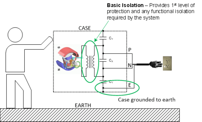
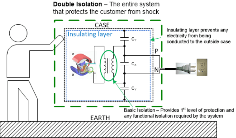
Simply put, isolation blocks unwanted DC and AC currents between separate parts of a system while transferring desired signals and/or power. Designers will apply isolation in many applications to power high-side gate drivers in power or motor-drive circuits, protect low-voltage circuits in high-voltage systems (such as processors in electrical automotive systems), separate communication between systems with different voltage potentials, or prevent electrical shock to end users of high-voltage equipment. Many different levels of isolation exist, including functional, basic, double and reinforced isolation.

Functional isolation, as the name suggests, merely provides a function. It passes a signal or power from a system at one voltage potential to another system and a different voltage. It does not protect against electrical shock.

Basic isolation is the next step up. It is functional isolation, but adds electrical shock protection. Class I devices use functional isolation along with an earth ground connection to protect users. Figure 1 shows a typical Class I device.

Figure 1: Typical Class I device

Double isolation takes a system with basic isolation (the basic level of protection against electrical shock) and adds a supplementary insulation layer between the electrical parts and the end user to reduce the likelihood of electrical shock in the event that basic isolation fails. Class II products require double isolation. These products are manufactured with AC plugs that do not have the earth ground prong on them, which improves the safety of the product because it does not depend on external wiring for user safety. Examples of end equipment with double isolation include grid asset monitoring systems, portable medical devices like IV pumps, and electrical devices like blenders or charging supplies for cellphones.

A second layer physically insulates internal metal parts (that could become live) from external casing, or uses a nonconductive external casing like plastic. Class II devices do afford some amount of safety vs. Class I devices because they do not depend on external wiring to provide redundant protection. Figure 2 illustrates a typical Class II device.

Figure 2: Typical Class II device

Reinforced isolation achieves the same result as double isolation using a single layer. A device with reinforced isolation provides basic isolation; plus, it is designed to ensure physical separation between printed circuit board traces, cores, windings, pins, etc., while meeting safety creepage and clearance distances (which refer to a physical distance between two voltage systems). A reinforced device is designed with double isolation, but can only be tested as a single piece.

Safety standards define values that must achieved for certification. For example, International Electrotechnical Commission (IEC) 60950-1 requires a creepage/clearance distance for basic isolation of 3.2 mm and a creepage/clearance distance for reinforced and double isolation of 6.4 mm. The voltage rating requirements for basic insulation are 2,500 VRMS for 1 minute and 3,000 VRMS for 1 second; for reinforced and double isolation, they are 5,000 VRMS for 1 minute and 6,000 VRMS for 1 second. You can see that reinforced/double isolation is exactly that – double the basic isolation. Double isolation devices are indicated on the label with a double-box insignia, as shown in Figure 3.

Figure 3: Double isolation insignia

Once you’ve decided to build a Class II device, you’ll need double or reinforced isolation. Why choose one type over another? The answer lies in the size and cost of your solution. As you could imagine, a single device that does the job of two lends itself to a physically smaller solution. You’ll achieve cost savings not only through integration into a single device, but in the reduction of engineering required to meet the isolation safety standard.

Fully integrated, reinforced isolation solutions are available in small packages, and they’re easy to implement. Such devices have several benefits compared to other solutions. For example, the Texas Instruments UCC12050 integrates all of the control, drivers, field-effect transistors and magnetics into a single package. You need only to place the device on the board with some bypass capacitors and follow the directions for proper board layout to design a reinforced isolated solution to bias supply applications in a super-small footprint. All of the engineering work has been done: no magnetics design, no supply controller selection.

Standards like Verband der Elektrotechnik (VDE) 0884-10 and International Electrotechnical Commission (IEC) 60747-17 provide the minimum requirements for reinforced isolation device certification. The UCC12050 fulfills all of the requirements for reinforced isolation, with minimum protections of 7 kVPK (for 1 second, production tested) and 5 kVRMS (for 1 minute) of isolation.

In summary, functional and basic isolation electrically isolate one voltage rail from another, while double and reinforced isolation offer interchangeable solutions to the same design goal – removing the earth ground pin from the plug.

Reinforced isolation provides a benefit over double isolation by reducing two insulating devices to one. It is a good choice in your system to save time, effort, space and possibly cost over other isolated bias supply solutions.

Additional resources:

4 trends in space-grade power management in 2020

$
0
0

Power architecture designs for space applications have historically lagged behind the commercial world due to the complexity of designing radiation-hardened integrated circuits (ICs). Today, the situation is changing rapidly. Developments in 5G are fueling the need for more bandwidth and global internet coverage, pushing many countries to launch higher volumes of satellites into space, while increased functionality and protection demands are driving the need for specialized space-grade power ICs that come in small packages and offer greater integration. As designers opt for more complex ICs for their space-grade power-management projects, here are four key trends to watch in 2020.

1. Higher power density in satellite payloads.

Modern satellites need to handle more onboard decision-making, requiring more bandwidth for data transfer and more secure data streams. As a result, satellite payload processing demands will continue to rise. This means that power requirements will continue to rise as well, as engineers expect higher power output capability from the same size board. The electronic components for space applications will get proportionally smaller, not only to support the high current requirements of the new generation of field-programmable gate arrays (FPGAs) that form the core of most satellite payloads, but also to meet the tight core voltage tolerance requirements of these FPGAs and to give designers more functionality in the same package size to achieve their design goals. TI’s TPS50601A-SP, the highest-power-density DC/DC converter IC in the market, is a 6-A, 7-VIN buck converter that is 50% smaller than similar solutions.

2. Increased integration of space FETs and smaller ceramic packages.

Along with higher power density, engineers designing power supplies for space-grade applications will continue to look for smaller solution sizes. One way to decrease the existing solution size is to integrate some of the high quantities of discrete field-effect transistors (FETs) and passives into a monolithic IC. This trend will grow in 2020, with high demand for products in known-good-die form or with more integration if in a ceramic package. For example, the TPS7H2201-SP is an eFuse with integrated protection features that can replace discrete solutions for cold sparing, overcurrent and reverse-current protection, and programmable current limiting. You can also expect to see smaller ceramic packaging – to the point where new package development is die-size-limited – as IC manufacturers look for ways to further shrink the power-supply size. 

3. More satellites with radiation-hardened power.

The growth of 5G networks is encouraging more countries to launch higher volumes of low-earth-orbit (LEO) satellites into space. These satellites are slated to be in space for less time than traditional satellites and therefore are exposed to less radiation. Thus, many satellite-makers are looking for a new class of products that offer some level of reliability and radiation performance at a lower price than traditional space-grade ICs. When designers try to achieve this by using a mix of radiation-hardened and commercial-off-the-shelf products, they often realize the importance of the power-stage architecture in ensuring the success of the mission. Transients can damage downstream devices, and designers will increasingly look for failure propagation mitigation in the power solution. The TPS7H2201-SP and TPS50601A-SP are examples of products in the critical power path that can help protect downstream devices from overvoltage and overcurrent. Another option is to consider Space Enhanced Plastic (Space EP) components, which are intended for short LEO missions, tested to a 30-krad total ionizing dose (TID), assured to 20-krad TID with radiation lot acceptance testing, and characterized to 43 MeV-cm2/mg for single-event latch-up (SEL).

 4The growth of in-depth radiation effects analysis and collateral.

The growth of more complex, integrated power ICs makes radiation testing, modeling and reporting even more important, and requires detailed evidence of an IC’s suitability for a space environment. Since the complexity of modern space-grade devices makes such analysis difficult, more designers will start to lean on suppliers for support, driving demand for detailed documentation for space-grade power-management devices, including radiation reports for TID, single-event effects (SEEs) and neutron displacement damage effects, as well as worst-case analysis (WCA) models. To answer this demand, more manufacturers will start providing full SEL, single-event upset (SEU), single-event transient (SET), single-event burnout (SEB) and single-event gate rupture (SEGR) characterization for devices, as well as worst-case analysis models, which include process-voltage-temperature variation, aging effects from life testing, TID effects, and which support Monte Carlo analysis. WCA models are available today for the TPS7H1101A-SP low-dropout regulator (LDO), the TPS7A4501-SP LDO, and the TPS50601A-SP buck converter.

Conclusion

Space application designers are demanding new, integrated technology that is in line with the commercial world but doesn’t compromise reliability and capability. These four trends are among many driving the development of cutting-edge space-grade power-management products, as well as detailed radiation reports and Qualified Manufacturers List Class V radiation-hardness-assured qualification to support both high- and low-orbit projects.

Additional resources:

Viewing all 4543 articles
Browse latest View live


<script src="https://jsc.adskeeper.com/r/s/rssing.com.1596347.js" async> </script>