Quantcast
Channel: TI E2E support forums
Viewing all 4543 articles
Browse latest View live

Using quad op amps to sense multiple currents

$
0
0

(Note: Paul Goedeke co-authored this technical article.)

Quad package operational amplifiers (op amps) offer good value in terms of cost per channel and can help save space on a printed circuit board (PCB) during layout. It’s common to use a multichannel op amp in applications such as three-phase motors and multiple LED strings, which sense multiple currents. However, using a quad op amp can introduce some complexities. In this article, I’ll discuss some PCB layout considerations when using quad op amps.

Figure 1 shows an example schematic, with generic current sources IS1, IS2 and IS3 representing the measured currents. Channels A and B are both unidirectional low-side current-sense circuits, each with their own gains. Channel D is a buffer for a reference voltage used by channel C in a bidirectional current-sense circuit.

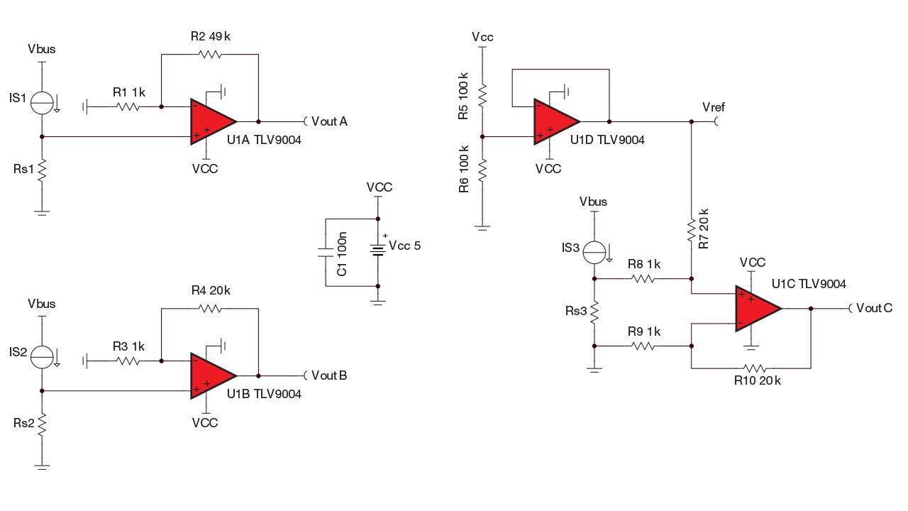
Figure 1: Multicurrent sensing schematic example

Figure 2 shows the same schematic but arranged around a shared, quad amplifier package. Careful layout is required to avoid turning floorplanning compromises into liabilities that impact circuit performance. Optimal placement for all channels may be difficult given the number of components and the need to place the sense resistors close to the device.

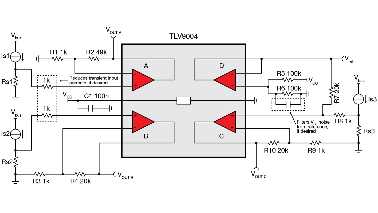
Figure 2: Example schematic shown around a shared amplifier package

Designs that measure multiple currents are more susceptible to parasitic inductances because of the amount of current flowing through the ground net. For example, a long, thin trace between the ground nodes of two components on a PCB will have a high parasitic inductance. High-frequency signals (such as noise or large transients) can turn small parasitic inductances into large impedances, which creates a potential difference between the ground nodes.

You can see this effect in Figure 3, which shows the channel D buffer circuit from Figure 1. A long trace between the ground node of R6 (shown in Figures 1 and 2) and the ground node of the op amp causes the parasitic inductance, shown as Lpcb. A transient creates a voltage delta across Lpcb, which means that the op amp and R6 are referenced to different potentials. For more information on PCB parasitic inductance, see the “Analog Engineer’s Pocket Reference” and “Analog Engineer’s Calculator.”

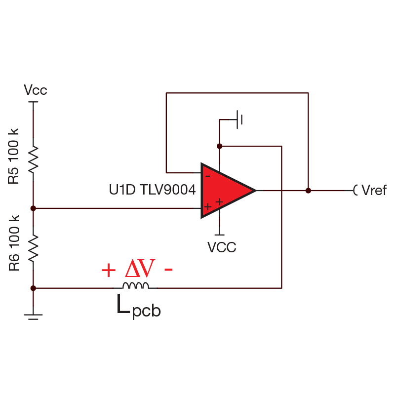
Figure 3: Parasitic inductance from PCB trace

To understand why these parasitic inductances can cause an issue, remember that the voltage across an inductor is determined by Equation 1, and that the current through an inductor cannot change instantaneously:

      (1)

Therefore, when a current transient occurs, the inductance of the trace fights the change in current and develops a voltage potential known as ground bounce. In some cases, ground bounce may cause device damage by violating the data-sheet’s absolute maximum limits for voltage and current.

In the case of the reference circuit on channel D (shown in Figure 3), ground bounce impacts the performance of the circuit by shifting the buffered voltage created by the R5 and R6 resistor divider. Channel C uses that value as a reference point, so any change in the reference impacts its output as well.

To reduce the effects of ground bounce and maintain system performance, keep these PCB layout considerations in mind:

  • Use Kelvin connections to the sense resistors to help eliminate the impact of parasitic trace and pad resistance in the measurement. Make sure that the sense traces are routed to the inside of the sense resistor footprint.
  • Try to keep the trace lengths to each sense resistor as short as possible and use balanced trace lengths for both Kelvin connections. If possible, move the sense resistors to achieve a better layout.
  • During layout, carefully consider the return current path:
    • Use ground planes to create a low-impedance return path.
    • When using a ground plane, make sure that no islands are created or that current is forced to take a long path around other traces. If necessary, connect with vias to a ground plane on another layer.
    • Keep a short path between the ground nodes of filtering and decoupling components and the ground node of the op amp.

In general, follow the best practices for current-sensing circuit layouts as discussed in the technical article, “How to lay out a PCB for high-performance, low-side current-sensing designs.” For general PCB layout considerations for op amps, read “The basics: How to lay out a PCB for an op amp.”

Let’s look at a couple of example circuit layouts using the schematic in Figure 1 and the Texas Instruments (TI) TLV9004 op amp in a 14-pin thin-shrink small-outline package. Figure 4 shows a nonideal PCB layout.

Figure 4: Example of a poor quad layout

Here are the major concerns with this layout:

  • The return path is made up of long thin traces.
  • No ground planes are used.
  • The sense resistors are far from the op amp and are not Kelvin connected.
  • The connections to the sense resistors have long, unequal trace lengths and differing widths.
  • The decoupling capacitor, C1, is far from the op amp’s VCC pin.
  • The supply voltage doesn’t pass through the decoupling capacitor before connecting to the op amp.
  • There are many more vias than the circuit requires, adding inductance and complexity.

Figure 5 shows the same nonideal layout but with the ground net highlighted. Notice the long trace between the negative supply pin of the op amp and the ground of R6 (as indicated by the white arrows). This is the exact scenario shown in Figure 3.

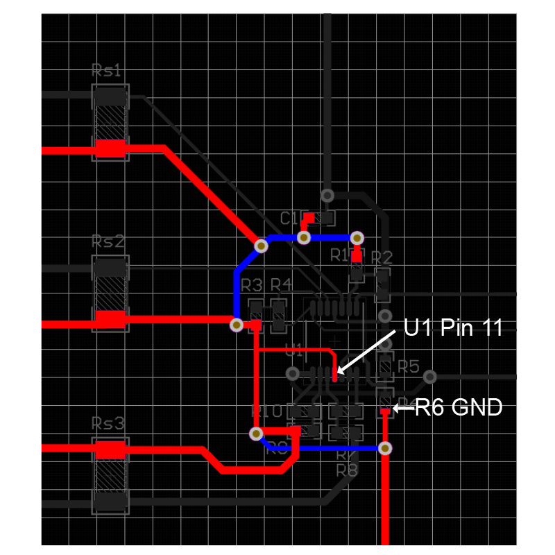
Figure 5: Example of a nonideal quad layout with the ground net highlighted

Figure 6 shows a well-designed PCB layout for this particular circuit. This new layout is much more compact and addresses the major concerns highlighted in the nonideal layout.

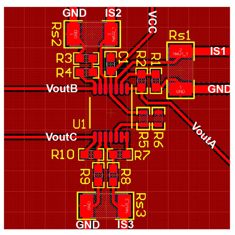
Figure 6: Well-designed layout for multiple current-sensing circuits

Some notable changes:

  • The components are placed close together to keep trace lengths short, reducing the susceptibility of noise coupling onto the traces.
  • Sense resistors are now close to the other components and use well-implemented Kelvin connections, as shown in Figure 7.
  • A ground plane provides a low-impedance return path.
  • The decoupling capacitor is placed as close to the op-amp supply pin as possible and routed such that the VCC trace must pass through the capacitor before connecting to the op amp.

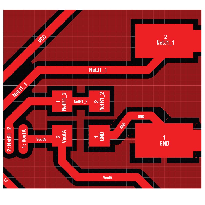
Figure 7: Kelvin connection detail

Using a quad package amplifier is often a good decision for a circuit design because it can help save cost and space on a PCB. Using the tips discussed above and the TI TLV9004 op amp, your quad amplifier circuit design can be successful. The 1-MHz TLV9004 has built-in electromagnetic interference and radio-frequency interference filters that can help improve a circuit’s resilience to interference. This device comes in package options ranging from an industry-standard 8.65-mm-by-3.91-mm small-outline integrated circuit package to an ultra-compact 2.0-mm-by-2.0-mm super-thin quad-flat no-lead package, making it useful for many types of applications.

Additional resources


How to choose the right thermistor for your temperature sensing application

$
0
0

There are thousands of thermistors on the market today, and finding the right one for your temperature-sensing application can be confusing. In this technical article, I’ll talk about some of the important parameters that you need to keep in mind when choosing a thermistor, particularly if you’re deciding between two popular types of thermistors for temperature sensing: negative temperature coefficient (NTC) thermistors or silicon-based linear thermistors. NTC) thermistors are frequently used due to their very-low price point, but they deliver low accuracy at temperature extremes. Silicon-based linear thermistors provide higher performance and high accuracy across a wider temperature range, but this typically comes at a higher price point.

The right thermistor for your application will depend on many parameters, such as:

  • Bill-of-materials (BOM) cost.
  • Resistance tolerance.
  • Calibration points.
  • Sensitivity (change in resistance per degree Celsius).
  • Self-heating and sensor drift.

BOM cost

Thermistors themselves are inexpensive devices. Because they are discrete, it is possible to alter their voltage drop through the use of additional circuitry. For example, if you are using an NTC thermistor, which is nonlinear, and prefer to have a linear voltage drop across your device, you may choose to add additional resistors to help achieve this characteristic. However, another alternative that would reduce BOM and total solution cost is to use a linear thermistor that already provides the voltage drop you want. The good news is that you can find both thermistor options at a similar cost thanks to our new family of linear thermistors, which help engineers simplify design, lower system cost and reduce printed circuit board (PCB) layout size by at least 33%.

Resistance tolerance

Thermistors are categorized by their resistance tolerance at 25°C, but that doesn’t quite tell the whole story of how they vary across temperature. It’s important to calculate the tolerance across your specific temperature range of interest by using the minimum, typical and maximum resistance values provided in the device’s resistance vs. temperature (R-T) table, which you can find in a design tool or data sheet.

To illustrate how tolerance varies with thermistor technology, let’s compare an NTC and our TMP61 silicon-based thermistor, which are both rated at a ±1% resistance tolerance. Figure 1 illustrates that as the temperature moves away from 25°C, both devices increase their resistance tolerance, but there is a very large difference between the two at temperature extremes. It’s important to calculate this difference so that you can choose a device that maintains a low tolerance for your temperature range of interest.


Figure 1: Resistance tolerance: NTC vs. the TMP61

Calibration points

Not knowing where your thermistor stands within its resistance tolerance span can decrease your system performance, because you need a larger margin of error. Calibrating will tell you what resistance values to expect, which can help you greatly reduce that margin of error. This is, however, is an added step in your manufacturing process, so you should try to keep calibration to a minimum.

The number of calibration points you’ll need depends on the type of thermistor you’re using and the temperature range of your application. For narrow temperature ranges, one point of calibration is fine for most thermistors. For applications requiring a wide temperature range, you have two options: 1) Calibrate three times using an NTC (this is due to their low sensitivity and high resistance tolerance at temperature extremes), or2 ) calibrate once using a silicon-based linear thermistor, which is significantly more stable than an NTC.

Sensitivity

Having a large change in resistance per degree Celsius (sensitivity) is just one piece of the puzzle when trying to obtain good accuracy from a thermistor. However, a large sensitivity won’t be very helpful unless you have the correct resistance values in software by either calibrating or choosing a thermistor with a low resistance tolerance.

NTCs have very large sensitivity at low temperatures given their exponential decrease in resistance values, but the sensitivity drastically decreases as the temperature rises. Silicon-based linear thermistors don’t have a large swing in sensitivity like NTCs, which allows for stable measurements across the whole temperature range. As the temperature rises, the sensitivity of silicon-based linear thermistors typically exceeds that of an NTC at about 60°C.

Self-heating and sensor drift

Thermistors dissipate power consumption as heat, which can affect their measurement precision. The amount of heat dissipated depends on many parameters, including the material composition and current passing through the device.

Sensor drift is the amount that a thermistor drifts over time, and is typically specified in data sheets via accelerated life tests given as a percentage change in resistance value. If your application requires a long lifetime of consistent sensitivity and accuracy, look for a thermistor with low self-heating and sensor drift.

So when should you use a silicon-based linear thermistor like the TMP61 over an NTC?

Taking a look at Table 1, you can see that for the same price, nearly any situation that is within the specified operating temperature of silicon-based linear thermistors can benefit from their linearity and stability. Silicon-based linear thermistors are also available in both commercial and automotive variants, and come in the standard 0402 and 0603 footprint packages common to surface-mount-device NTCs.

ParameterNTC thermistorsTI silicon-based linear thermistor
BOM cost

Low to mid:

  • Low cost for the thermistor
  • May require extra linearization circuitry

Low:

  • Low cost for the thermistor
  • No need for extra linearization circuitry
Resistance tolerance

Large:

  • Big difference between tolerance at 25°C and temperature extremes

Small:

  • Small ±1.5% maximum tolerance across the whole temperature range
Sensitivity

Inconsistent:

  • Very large at low temperatures
  • Drastic decrease with rising temperatures

Consistent:

  • Stable sensitivity across the whole temperature range
  • Greater than NTCs typically above 60°C
Calibration points

Multiple:

  • Multiple points needed for wide-range applications

One:

  • Only one point needed for wide-range applications
Self-heating and sensor drift

High:

  • Increased power consumption with temperature
  • Large sensor drift

Minimal:

  • Decreased power consumption with temperature
  • Small sensor drift

Table 1: NTCs vs. TI silicon-based linear thermistors

For complete R-T tables of TI thermistors and easy temperature conversion methods with example code, download our Thermistor Design Tool.

Additional resources

Driving HVAC system flaps with an integrated, multichannel motor driver

$
0
0

Automotive heating, ventilation and air-conditioning systems (HVAC) systems contain multiple flaps, each driven by a corresponding motor. Integrated, multichannel motor drivers give designers the ability to drive multiple motors independently in both directions. Having the ability to drive all motors (also known as flap actuators) from a single device saves not only board space but also cost, albeit introducing challenges.

One design challenge when integrating multiple half bridges in one device is how to handle the thermals of the integrated field-effect transistors (FETs) in the operating ambient temperature range. Driving multiple motors with the least amount of pulse width modulation (PWM) signals is a complex task. There are cases where one of these multichannel devices is not enough to drive all of the HVAC system flaps, and multiple device communication setups are required.

Another design challenge is how to control the movement speed of the flap loads. This speed control is typically achieved using a pulse-width modulation (PWM) drive, which requires the generation of PWM signals within the device.

To solve these challenges, TI created the integrated, multichannel DRV8912-Q1 motor-driver family. These drivers can drive up to six motors simultaneously in both directions or up to 11 motors separately in a single integrated circuit. Figure 1 shows the pinout of the device, highlighting its integration of 12 half-bridge outputs, the use of Serial Peripheral Interface (SPI) communication and no PWM input pins.

Figure 1

Figure 1: DRV8912-Q1 package


Drive more motors with fewer brushed-DC drivers

 Reduce design time and increase reliability in your automotive HVAC design with the DRV8912-Q1 family of scalable, multi-channel brushed-DC motor drivers with advanced diagnostics. 

Thermal performance

Thermal management, which is managing the die temperature of the device, is one of the biggest challenges with integrated multi-half-bridge drivers. Figure 2 shows the low drain-to-source on-state resistance (RDS[on])of the integrated FETs in the DRV8912-Q1 motor-driver family across an ambient temperature (TA) and with an operating voltage range from 4.5 V to 32 V. The ability to drive multiple loads while keeping the die temperature below 150°C is essential for a multi-half-bridge device in HVAC systems.

Figure 2: High- and low side RDS(on) vs. TA

Daisy-chain communication and PWM generators

For cars that have multiple HVAC zones and options, there could be a need for multiple devices to drive a large number of flap actuators. This does not mean that you need to increase the number of microcontrollers in your design, however, as the DRV8912-Q1 family does daisy-chain in SPI-based communication. As shown in Figure 3, one microcontroller is a master communication device, and multiple drivers are slaves using a single SPI communication. This feature of the motor driver reduces hardware expenses and overall system size.

 figure 3

Figure 3: MCU to flaps with daisy-chain

Speed control is a benefit of using PWM control in HVAC systems. The motor drivers in the DRV8912-Q1 family have four integrated PWM generators. These generators enable the configuration of duty cycle and frequency, as well as PWM generator assignments to one or more channels. For example, you can assign one PWM generator to half bridges 1, 3, 5 and 6, while assigning a second PWM generator to half bridges 2 and 4. This setup enables you to drive up to two groups of loads with two PWM generators.

Advanced diagnostics in HVAC systems: open-load detection

Open-load detection (OLD) is a diagnostic feature that determines whether or not there is an open electrical circuit between the HVAC control module and the flap motor. In HVAC systems, disconnected load detection is challenging because the current required to drive the motor changes when the airflow changes. These current changes can cause false open-load faults.

The DRV8912-Q1 motor driver family provides four types of OLD diagnostics to meet HVAC load disconnection diagnostic needs:

  • Active OLD. Active OLD ensures a driver-to-motor connection when the motor is driving. Figure 4 is an example where the OLD current threshold, IOLD, must drop below the motor current, IOUTx, for a duration larger than tOLD to cause an OLD event. Fault clearing occurs when IOUTx becomes greater than IOLD. This OLD diagnostic gives you the ability to detect load disconnections while the load is driving and stops the system from continuing operation. 

figure 4

Figure 4: Active OLD operation

 Low-current active OLD. The OLD current threshold is around one-tenth the magnitude of the active OLD current threshold. In HVAC systems, the airflow traversing through the driven flaps causes the motor to require less torque (current) to drive the flaps. The motor’s driving current could drop to a value below the IOLD of active OLD, creating a false OLD flag. With a lower OLD threshold, driving motors when the required drive current is less than the active OLD current threshold can prevent false OLD flags from occurring.

  • Negative-current active OLD. When the current OLD threshold is negative, this diagnostic uses the current recirculating through either the body diode of the recirculation FET or the FET itself to prevent a false OLD flag seen in active OLD. Figure 5 shows the false flag occurring with negative current enabled in Figure 5a, and the flag prevented without negative-current enabled in Figure 5b.

Figure 5: False OLD flag during high-side current recirculation with (a) and without (b) negative-current enabled 

  • Passive OLD. Passive OLD detects an open-load condition before the driver outputs are enabled. All of the FETs are in a high-Z state, while a minimal amount of diagnostic current flows through the load for a short amount of time to test the load’s connection to the FETs. The diagnostic current must be minimal to avoid load rotation. With this OLD diagnostic, you can detect a motor disconnection even if the motor is not driving.

Simplifying flap driving

HVAC systems vary in complexity and automation level, depending on vehicle class. The DRV8912-Q1 family is pin-to-pin compatible between all devices. With low RDS(on) for thermal performance, SPI daisy-chaining, internal PWM generation and unique open-load detection, the benefits of the DRV8912-Q1 device family for HVAC systems are numerous.

Additional resources:

Exploring evolving trends in automotive cluster audio design

$
0
0

Automotive instrument clusters are in the middle of a revolution. The cluster is rapidly becoming a part of the larger infotainment ecosystem. Consumers are driving around with intelligent, quickly evolving displays on their dash, but the audio chimes – the essential driver alerts that come from a speaker housed inside the cluster – are lagging behind.

Cluster audio does not get the attention that a vehicle’s central head unit audio gets. Advances in low-power audio technology are enabling new trends in cluster systems, however.

Out with the old

Analog gauge clusters are a dying market, replaced in most vehicles by a hybrid cluster featuring digital displays. However, discrete audio amplifiers – the source of the chime in these ancient electromechanical clusters – have stuck around, in spite of the vast leaps in automotive audio technology.

Discrete amplifiers emit a sound resembling a weak buzz more than a proper audio signal. The microcontrollers responsible for controlling the whole cluster often have only one output pin to spare for generating a pulse-width modulated (PWM) audio signal. After passing through a low-pass filter, the signal becomes a simple sine wave, which is amplified by a discrete amplifier. The sound is often overdriven in order to achieve the sound pressure levels (SPLs) that the vehicle manufacturer requires.

Replacing the discrete amplifier with an integrated audio amplifier (Figure 1) is a simple but rewarding design change. For example, feeding the same signal into the input of the TPA6211A1-Q1 Class-AB amplifier provides the benefits of:

  • Louder, clearer sound – integrated amplifiers can output audio at much higher output power levels (3 W of power from a 5-V rail) without distorting, meaning louder (higher SPLs) chimes and less harmonic distortion and noise (THD+N).
  • Simpler design – discrete amplifier designs can use up to four transistors and up to eight passive components per channel, which in some cases puts a discrete design in the same cost range as an integrated Class-AB amplifier. The simpler integrated solution might actually save money in the long run.

Figure 1: Example discrete amplifier circuit with low-pass filter (left) and integrated amplifier with low-pass filter (right)

The digital cluster chime

Engineers who have embraced the benefits of integrated audio are advancing what solid-state instrument clusters and the audio chime can do for drivers. For example, advanced driver-assistance systems (ADAS) make use of the cluster speaker in some vehicles to provide an auditory warning when drivers need a reminder to remain alert. Common driver errors, such as drifting out of their lane or failing to check their blind spot, cannot be fixed by a loud chime, but chimes can help give the driver an extra sense of what is happening around them. It is possible to make forward collision, blind spot and lane departure warnings more effective by using the cluster chime to alert drivers without forcing them to divert their eyes from the road.

These advanced features are made possible by the adoption of advanced automotive processors, such as TI’s Jacinto DRAx digital cockpit systems-on-chip (SoCs), which operate the cluster displays in hybrid and solid-state clusters. Processors with memory open up the possibility of storing digital waveforms. Rather than rely on a single pin for audio output, digital processors use an I2S bus, possibly as an FPD-Link channel, to send the digital audio data to the speaker amplifier. This increases the range of sounds that a cluster can make.

Digital audio amplifiers provide a huge benefit in such systems, eliminating the need for a digital-to-analog converter to convert I2S to audio. As Figure 2 shows, introducing a digital input amplifier to a cluster design can open up the possibilities for chime alerts with little additional cost and only simple design changes.

Figure 2: Digital amplifiers simplify design by integrating power and data converters, essential elements for higher-end audio chimes

Load diagnostics

Load diagnostics are a major concern for automotive audio systems. During production or in use, the speaker wiring can become disconnected from the speaker (an open load condition), create a short between the wires (a terminal short condition), or come in contact with the voltage rails (a short-to-ground or short-to-power condition). All of these events can damage the amplifier and speaker if not detected quickly. Damaged audio systems are not only expensive but can be hazardous to drivers in a vehicle that uses the cluster chime for ADAS warnings.

Automotive amplifiers have begun to integrate load diagnostics to help lessen design challenges and costs. Amplifiers with integrated load diagnostics notify the cluster processor of the fault and can mute or shut down the device as necessary to prevent permanent damage to the device or speaker.

Sounds good – what’s next?

With all of the advances in automotive technology, what’s next for the instrument cluster, and what does that mean for the audio chime? For some manufacturers, it means louder, clearer and more immersive audio experiences.

Some manufacturers are moving toward integrated cockpits, which bring the cluster processor into the head unit. The processor generates the graphics, which are sent via FPD-Link to a remote cluster display in the familiar space behind the wheel. I2S signals from the processor can be sent via FPD-Link to the cluster audio amplifier. Cluster chimes can also be amplified by a spare channel in the infotainment amplifier, bringing the cluster’s audio into the head unit as well.

Modern drivers are now accustomed to the bells and whistles in their vehicles that make the driving experience safer and more fun. Designing clear, robust cluster audio systems is simple yet critical. With that in mind, how can you afford not to use the best low-power integrated audio amplifiers available?

Additional resources

Three questions to ask about wireless BMS for hybrid and electric vehicles

$
0
0

(Dan Torres co-authored this technical article.)

Lithium battery cells are continuously getting more affordable and energy dense, and can drive hybrid electric vehicles (HEVs) and electric vehicles (EVs) farther, longer. With these advancements, automotive design engineers can now turn their attention to further enhancing efficiency by reducing the size and weight of the battery management system (BMS).

For background on battery management systems, see “HEV/EV battery management systems explained simply.”

The traditional wired BMS architecture connects battery packs using wire harnessing in a daisy-chain configuration, which is cumbersome to manufacture, often requires maintenance, and is difficult to service.

To overcome these challenges, an evolution to wireless BMS shows potential, with wireless chipsets working in conjunction with battery monitors to communicate and pass voltage and temperature data from each cell to the main microcontroller in the system. The inherent reduction in the number of required cables and harnesses lowers vehicle weight and saves costs.

Figure 1 is an example of a wireless BMS architecture.

Figure 1: TI’s wireless BMS architecture

If you’re exploring the idea of switching to a wireless BMS architecture, here are three key questions to consider:

1.      Is it reliable?

Although wireless communication is already replacing cables in various applications, one critical point to consider is the reliability of the wireless link and network. You can quantify reliability using packet error rates and the probability of successfully sending a message between a transmitter and a receiver. This probability should be 99.999%, with a packet error rate of 10-6.

2.      Is the wireless BMS safe for passengers, mechanics and property?

A wireless BMS should accurately monitor conditions and respond quickly, reliably and safely if a hazardous event is detected to mitigate danger or destruction. Ideally, the system should meet requirements up to Automotive Safety Integrity Level D, which is the highest functional safety goal defined by the International Organization for Standardization 26262 road vehicle standard.

3.      Is it secure?

Will a wireless BMS work if someone attempts to tamper with the vehicle’s battery system? Look for systems that provide encrypted messages, using security enablers such as cryptographic accelerators with key exchange and refreshment mechanisms, message integrity checks and debugging security.

Bonus question! Which is best: wired or wireless BMS?

This is a trick question, because either a wired or wireless BMS may be appropriate for your design, depending on your automotive architecture and design goals. Table 1 compares the main differences between a wired and wireless system.

Considerations

Wired BMS

Wireless BMS

Weight

Wiring increases overall vehicle weight.

A wireless system decreases vehicle weight.

Design flexibility and serviceability

Less flexibility with a larger footprint overall; more difficult to service.

Larger overall footprint; less flexible system design due to cumbersome wires, difficult to service.

Smaller footprint enables more flexibility with a simpler design and placement within the vehicle. Easier to service.

Measurement

Time-synchronized measurements of voltage and current can be a difficult design challenge.

Wireless systems naturally enable time-synchronized measurements and provide the ability to add more synchronized sensing capabilities.

Reliability

Wiring harnesses tend to break over time; they are difficult to repair and require rewiring of battery packs.

No wires to maintain; design has to overcome harsh automotive radio-frequency environments and non-line-of-sight challenges.

Security

Contained and fully secure system communication.

Possible to breach poorly designed systems that lack security protocols.

Table 1: Comparing aspects of wired and wireless BMSs

Wired battery management systems are tried, true and not going anywhere soon; but wireless BMS are the next evolution. In fact, with Strategy Analytics estimating 36 million EVs on the road by 2026, wireless BMS offer promising ways to make vehicles more efficient and reliable – features that appeal to both original equipment manufacturers and consumers.

Watch this video to learn more about wireless BMS and see a demo. 

(Please visit the site to view this video)

Adjusting VOUT in USB Type-C™ and wireless charging applications, part 2

$
0
0

As I discussed in the first installment of this series, one option to control output voltage (VOUT)for USB Type-C Power Delivery (PD) and wireless charging applications is to use switching resistors. This article will explain a different approach that requires fewer components and signal lines called modulated voltage programming.

Modulated voltage programming

You may recall from part 1 that switching resistors require three switched resistor branches and three control signals to produce the four voltages needed for USB Type-C PD applications. Each switched resistor branch also requires a resistor-capacitor (RC) delay to control the speed of switching, in order to prevent falsely triggering the overvoltage protection (OVP) function of the four-switch buck-boost controllers. The actual hardware requires many additional components, and the solution can appear cumbersome and may not easily fit into compact designs. In such cases, you may need a different approach to reduce the number of components.

Figure 1 shows an example in which a modulated voltage source (VC) alters the feedback (FB) pin voltage. Therefore, Equation 1 determines the VOUT:

where VREF is the controller error amplifier reference voltage. Decreasing or increasing VC will adjust VOUT up or down, respectively.

There are two ways to control the VC level with a microprocessor. The first is to use an integrated digital-to-analog converter (DAC), and the second is to directly use the pulse-width modulation (PWM) signal produced by the microprocessor.


Figure 1: Adjusting VOUT with a modulated voltage source

Controlling voltage through a DAC

USB Type-C PD and wireless charger systems usually have a microprocessor with an internal DAC. If it does not have an internal DAC, an external one like TI’s DAC43401 or DAC53401 can be used. As shown in Figure 2, the DAC can produce the required VC to adjust VOUT by programming the microprocessor to follow Equation 1.

False VOUT OVP can be a problem if the slew rate of VC is too quick. Therefore, when using microprocessor to control VC, make sure that the VC transition time is longer than the buck-boost DC/DC stage loop response time but does not exceed the applicable USB Type-C specifications.


Figure 2: Using a DAC to control the VC

Controlling voltage through a PWM signal

The second approach is to use a General-Purpose Inputs/Output port (GPIO) of the microprocessor to produce a PWM signal. This PWM signal can be filtered out by an RC filter to produce a DC voltage before being fed into the FB pin, as shown in Figure 3. Changing the PWM duty cycle can dynamically adjust VOUT.


Figure 3: Adjusting VOUT through the PWM signal

The PWM filter will, however, introduce ripple voltages. If the low-pass corner frequency of the RC filter is much lower than the frequency of the PWM signal, both R3 and the FB pin will see an almost pure DC voltage. Therefore, the PWM will not cause significant ripples on the VOUT rail. I recommend choosing R4 and C1 such that the RC filter’s corner frequency is set to at least two decades below the frequency of the PWM signal, such that the ripple voltage at FB pin can be attenuated by at least 40 dB. Consequently, the selection of R4 and C1 should satisfy Equation 2:

where fPWM is the frequency of the PWM signal.

Assuming that the PWM signal’s duty cycle is D, the valley voltage is 0 V and the peak voltage is VPWM, then VOUT will satisfy Equation 3:

Using two-stage RC filters to avoid excessive delays

As mentioned above, the RC filter needs to attenuate the PWM by at least 40 dB. If the PWM signal frequency is limited, say to 200 kHz, the RC filter’s corner frequency will have to be set at 2 kHz, implying an RC filter time constant of about 80 ms. Since the settle time of an RC filter takes four times the time constant, the response to a step duty-cycle change will take more than 320 ms to settle, much longer than the USB Type-C PD specification of the voltage transition time. A solution is to use a two-stage RC filter, as shown in Figure 4.


Figure 4: A two-stage RC filter to reduce the delay time

A two-stage RC filter provides 40 dB of attenuation per decade. In the same example, where the PWM signal is at 200 kHz, the filter’s corner frequency can be raised to 20 kHz, reducing the filter’s time constant to only 8 ms. The response to a step change of duty cycle will settle down within just 32 ms, which is fast enough to meet the USB PD applications. In general, choose the RC filter according to Equation 4:

Now, VOUT and the PWM duty cycle (D) satisfy Equation 5:

Note that VOUT will increase when D decreases. Programming the microprocessor according to Equation 5 will produce a PWM signal with the correct duty cycle to regulate the four-switch buck-boost output to the desired voltage level appropriate for a USB Type-C PD application.

Conclusion

For every technique showcased in this series, it is important to remember that false OVP events are possible if the switching between voltage levels is too quick. So make sure that the transition time is sufficient enough to satisfy the application and not trigger a false OVP event.

Additional resources

Exploring connectivity trends for Bluetooth® Low Energy in the car

$
0
0

Connectivity’s ubiquity in the world is certainly gaining momentum in the automotive industry. Many car owners think of automotive wireless connectivity as a simple interaction with an in-car infotainment system, but new applications are emerging, whether it’s personalizing an owner’s interaction with the vehicle, creating a path for lower-power connectivity operation when in the key-off state, or providing users the experience of passive entry via phone-as-a-key (PaaK) applications. 

For several years now, TI’s Bluetooth® Low Energy technology has been connecting multiple elements within the car, including head units, tire pressure monitoring systems (TPMSs), telematics control units (TCUs), car access through PaaK and other accessories.

In 2014, TI created the CC2541-Q1 device, followed by the CC2640R2F-Q1 device in 2017 and now the CC2642R-Q1 device, which features 352 KB of available flash space and an Arm® Cortex®-M4F processor core, while maintaining the same low-power performance as the previous platforms. The device works in combination with the SimpleLink™ software development kit (SDK).

Let’s break down a simple example where TI Bluetooth Low Energy device are being used today. One of the latest trends is the use of Bluetooth Low Energy for car access via PaaK applications. This where a a vehicle owner can pair their phone with the car via Bluetooth, then the car and phone passively connect to one another to locate the phone and unlock the vehicle for permitted users. When designing car access systems, there are certain quality and reliability requirements needed. For example:

  • Reliable interoperability with smartphones
  • High performance in noisy and challenging environments
  • AEC-Q100 qualified hardware
  • Software development process that meets high industry standards for quality
  • Low-power consumption in the key-off state

With the CC2642R-Q1 device, in combination with TI’s Bluetooth 5.1 stack in the SimpleLink SDK, you can leverage the sub-1-µA standby current, low-power transmit and receive currents (7.3 mA and 6.9 mA, respectively) and gain robustness, range and reliability in data transmission using the coded physical layers provided in the Bluetooth 5 specification.

Another use case where low power is a big requirement is in TCUs. Often, TCUs comprise high-power-consuming connectivity devices or elements such as cellular modems, Wi-Fi® and many other types of connectivity, depending on the vehicle. When the vehicle is in the key-off state, there are stringent power budgets that the vehicle must maintain in order to not drain the battery.

Therefore, some sort of system is required that allows the vehicle to shut off the higher-current-consuming components of the vehicle but still wake up when needed. While there are several options for connectivity within the car, Bluetooth Low Energy is a great option for quality and reliability. It is often used as a way to enable the TCU to determine whether it needs to wake up to handle software updates or any other diagnostic functions. TI envisions the trend of using Bluetooth Low Energy to connect applications within the car will continue to increase as vehicles become more technologically advanced and connected.

Additional resources: 

(Please visit the site to view this video)

MIOTY, the new LPWAN standard, provides quality and scalability for worldwide Sub-1 GHz communication

$
0
0


Wireless technologies are the backbone of our rapidly evolving, connected world. These technologies push different boundaries around communication speed, range and integration. Developers and manufacturers are looking for standardized solutions that offer a simplified approach to Internet of Things (IoT) design.


While communication speed has been a priority for decades, there’s been a stronger focus lately toward long range and low power connected devices. The networks long-range, low-power devices use are often referred to as low-power wide-area networks (LPWANs). Examples of applications that benefit from LPWANs are environmental sensors like temperature and air quality and battery-powered flow meter sensors for water, heat and gas.


These sensors typically communicate very infrequently – with minutes to hours between each engagement. For such applications, the technology is optimized for long-range radio-frequency (RF) communication at the expense of high data throughput.


Today, LPWAN solutions have a lack of scalability and are less robust due to interference issues and coexistence problems with other radio networks. Many existing solutions are not able to offer very high data delivery consistency over time. Battery life is also limited due to inefficient transmission methods.


TI is one of the founding members of the recently formed MIOTY Alliance, which serves as the governing body of the MIOTY LPWAN solution. The MIOTY standard offers a complete long-range and low-power solution for worldwide Sub-1 GHz communication


MIOTY can help IoT developers overcome design challenges such as:

  • Difficulty meeting long-range requirements Achieving long battery lifetime

  • Performance degradation in high-node-count networks.


MIOTY has many inherent advantages, including:

  • A combination of coding and narrowband operation enables long rage RF communication.

  • Reduced packet overhead and efficient coding result in current saving.

  • More robust communication and larger networks are possible due to the telegram splitting.


The MIOTY solution offers a star network for low-power end/leaf nodes, as well as a gateway solution for cloud connectivity. As of today, MIOTY offers a private network, but the expectation is that third parties will also offer a network solution as a service.


The MIOTY standard operates in license-free bands around the world. There are no costs involved in using the radio spectrum, unlike narrowband IoT (NB-IOT) solutions.


Standard vs. proprietary solution

The answer may seem obvious, but existing LPWAN solutions on the market today are suffering from a lack of standardization; some are driven by startup companies with an unproven track record. It isn’t easy to make alterations to an RF protocol or system if you need to reverse the compatibility of an existing product, so it’s important to choose the right solution now and for the future.


The basic MIOTY technology (physical layer [PHY]/Media Access Control) is based on a public technical standard by the European Telecommunications Standards Institute (ETSI) (TS 103 357) and can be downloaded by anyone at no cost. MIOTY has already been tested with three independent silicon providers, including Texas Instruments, using the CC1310 microcontroller (MCU).


Key benefits of MIOTY technology

MIOTY technology is a good fit for long-range, low-power and robust networks. It can scale to large networks and reach 5 km in urban areas.


Existing LPWAN solutions give the impression that there are multiple silicon providers available, but a more careful look reveals that some solutions use RF transceivers from only one or two companies – representing vendor lock-in. MIOTY is transparent with respect to important details like modulation formats (PHY). MIOTY solutions have already been tested with multiple vendors, which helps create real competition in the marketplace.


TI offers a complete family of products for MIOTY. The CC1310 wireless MCU, part of the SimpleLink™ platform, is an ultra-low-power system-on-chip that includes an RF transceiver and an Arm® Cortex®-M3 MCU plus peripherals. This device can fit a complete MIOTY stack as well as a small sensor application in a 4-mm-by-4-mm quad flat no-lead package. Larger memory and higher processing power alternatives are CC1312R and the CC1352R. CC1352R can in addition to handling sub 1 GHz MIOTY, also handle a Bluetooth Low Energy connection to a smartphone.


MIOTY is truly the LPWAN solution for the future. It offers scalable, robust network performance, which is a core requirement for industrial IoT. In addition, the MIOTY standard provides low power due to effective system architecture. When combined with the low power SimpleLink RF SoC, this architecture makes long battery life possible. As the IoT landscape continues to grow and evolve, the MIOTY standard and the SimpleLink platform create a viable connectivity option for worldwide Sub-1 GHz communication.


Visit www.mioty-alliance.comto learn more about MIOTY technology.


How a look-ahead boost conquers battery-life challenges in speakers

$
0
0

Life is hard for audio system designers under pressure to design speakers with a longer battery life. “It doesn’t play as long as I wanted” is feedback no marketing team wants to receive.

One easy way to extend battery life is to increase the size of the battery. Yet few systems can bear the increased cost of a larger battery, so selecting a larger battery with more milliampere hours is out.

Another design approach necessitates spending inordinate amounts of time searching for that magic combination of key components like boosts, microprocessors, radio-frequency modules and amplifiers with low power consumption.

Project development time may be too short (or resources too few) to do much more than tweak the current design. Frequently, a design ends up with a simple, constant-output boost to increase the voltage from a 1S battery to 12-V rail to drive a cheap, inefficient TV amplifier at 10 W.

Ironically, a major contributor to the power problem is that cheap, inefficient TV amplifier. Those amplifiers were designed years ago for TVs and speaker bars, both powered by a 24-V regulated rail. But solutions borrowed from yesterday do not translate well to battery-powered designs. Battery life suffers more when a constant-output boost converter continually drains a 1S battery to generate a 12-V rail, even when idling.

Einstein once said that the thinking that created the problem isn’t the thinking needed to solve the problem. So using Einstein for inspiration, consider replacing your regular boost converter with a look-ahead Class-H boost converter and replace the TV amplifier with a higher-efficiency amplifier designed for battery-powered systems. You’ll get bonus points if the entire solution is integrated into one device!


Looking for high efficiency in small speaker applications?


Learn more about the TAS2562 audio amplifier with Class-H boost

The look-ahead processing matches the power consumption to the audio output by constantly analyzing the audio signal and keeping the power within a small envelope of power use, then managing the boost output. This envelope-tracking approach reduces audio power consumption as much as 40%. It also lowers the system bill of materials (BOM) by removing extra components. You can read more about Class-H boost in the application note, Benefits of Class-G and Class-H Boost in Audio Amplifiers.

TI devised a test to compare a look-ahead boosted solution to a constant-output boost converter. Our test comprised these steps:

  1. Fully charge the 1S battery of the original solution.
  2. Connect a TI battery monitor evaluation module to track battery life.
  3. Run the speaker at full volume until the battery dies.
  4. Repeat the process with the same conditions using a Class-H boost converter.

Figure 1 shows how this the look-ahead boost works: the upper half of Figure 1 shows the battery life of the original boosted amplifier with constant output, while the lower half of Figure 1 shows what a look-ahead Class-H boost can do.

Figure 1: TI’s look-ahead Class-H boost reduces power consumption 40%

Figure 2 shows what is happening moment by moment as music plays.

Figure 2: TI’s look-ahead Class-H boost uses half a Watt less power on average

The look-ahead boost converter tracks the incoming signal using sophisticated algorithms that manage the power level; it increases and decreases the boost to match the voltage that the amplifier needs. Its capabilities are similar to what you do when driving: you watch the road ahead, then accelerate, coast or brake to match the conditions.

The look-ahead Class-H boost converter controls power consumption in battery-powered systems; our tests and power-consumption comparisons show that this approach is easy and effective. The converter increases battery life and reduces BOM cost because you can drop the external boost and possibly reduce the battery size as well.

For some designers, these two changes alone more than pay for the cost of the amplifier. That’s why leading audio brands have this built their own version of a look-ahead boost into their systems and are getting more bass, louder music and longer battery life.

You could emulate the leading brands by creating an effective look-ahead boost control. It takes a bigger processor, a variable boost and software development to track the audio signal and calculate the power needed by the amplifier at just the right moment. It isn’t impossible, but it takes time and expertise, and increases BOM.

TI has done all this work for you. These amplifiers start with a 90% efficient Class-D amplifier, then integrate look-ahead processing, a multilevel boost and a tracking algorithm. And with easy-to-use control software, PowerTune amplifiers are a simple path to longer battery life, lower BOM and reduced development time.

Additional resources

Rich and Mary Templeton give $51 million to transform engineering at Union College and recruit more women to tech careers

$
0
0

Rich and Mary Templeton have given $51 million to their alma mater, Union College, to transform its engineering and liberal arts programs and help recruit more women into technology careers, a challenge our company has long been devoted to solving.

The donation from our president, chairman and CEO and his wife - the largest gift in Union's 225-year history - will be used to create the Templeton Institute for Engineering and Computer Science. It will also be used to hire additional engineering faculty and broaden the curriculum. The announcement of the gift was made on Feb. 21 during a ceremony at the school.

"The greatest thing we can do to impact community is to build great educational institutions that are equipping students for the future," Rich said. "Mary and I were fortunate to be educated by Union, a wonderful college that did a great job of preparing us for successful careers."


Rich and Mary Templeton met at Union College.

In making the gift, Rich and Mary are honoring a legacy of giving instilled in them by Texas Instruments' founders and leaders.

"Mary and I have had the privilege of learning about giving and community impact from people like the late Margaret McDermott, wife of TI founder Eugene McDermott, who selflessly gave of her time, treasure and talents over six decades to make a difference," Rich said. "We are grateful to follow the example set for us by generations of leaders who were determined to make TI a company that we can all be proud to be a part of and proud to call our neighbor."

Rich and Mary were 17 when they met at Union in Schenectady, N.Y. They took freshman calculus together and became good friends while he helped her with homework. He joined our company after earning a bachelor's degree in electrical engineering. Mary, a philanthropist and community volunteer, graduated with a bachelor's degree in computer science.

"We want to be very thoughtful and deliberate about philanthropy and what types of investments could make the biggest differences that would be impactful - not just today, but in the future," Mary said. "For that reason, we feel very strongly about education. If you educate, it's the old adage: If you teach a person to fish, they'll eat for life."

"The founders of TI were our inspiration to
become active philanthropists."
– Mary Templeton


Rich and Mary Templeton speak to female engineering students in a roundtable discussion at Union College.

'This allows us to be innovative in our teaching'

Union is among a handful of liberal arts colleges in the U.S. that offer an engineering curriculum. Rebecca Cortez, Ph.D., professor of mechanical engineering and director of Union's engineering program, hopes that adding more dedicated engineering faculty members will encourage cross-collaboration among staff to expose a wider range of students to math and science.

"The support from the Templetons will strengthen our current engineering program," she said. "This allows us to be innovative in our teaching. Engineering faculty can teach courses with some of our humanities and social science colleagues, bringing new perspectives to students."

Union leadership will also explore broadening its course offerings to include areas that may attract more female students to engineering. Sarah Taha, a recent Union graduate who earned a scholarship to study biomedical engineering, said she was the only woman in some of her engineering classes. She hopes the gift will also be used to create scholarships that bring more women into the program. "Union really focuses on equality," Sarah said. "I think having a specific scholarship for women would be a win. Mine helped me become the woman I am today."

Inspired by a legacy of giving

Mary and Rich carry forward a long-held TI tradition of giving back.

They give generously to educational institutions and other organizations in the community, and also co-led the 2018-2019 United Way of Metropolitan Dallas' campaign, which raised more than $61.6 million.

"Mary and Rich Templeton are tremendous examples of what we want for all our students at Union College," said David Harris, president of Union. "I am grateful that they appreciate they were more prepared for careers and life because they majored in engineering and computer science at a school that emphasizes the liberal arts, and even more so that they are committed to ensuring future generations have similar opportunities."

Mary hopes their commitment to giving back will inspire others to do the same.

"The founders of TI were our inspiration to become active philanthropists," Mary said. "I hope that years from now someone says we inspired them to give of their time, talent and treasure. That would be a wonderful legacy."

Designing with linear thermistors

$
0
0

The same hardware and software design methods commonly used with other positive temperature coefficient (PTC) or negative temperature coefficient (NTC) thermistors also apply to silicon-based linear thermistors. In this technical article, I’ll cover some simple hardware and software methods when using silicon-based linear thermistors.

Hardware

One method to generate an output voltage across a silicon-based linear thermistor is to use a voltage divider circuit, as shown in Figure 1. This results in a positive and linear voltage drop ( ) response, which is most often routed directly to the analog-to-digital converter (ADC).


Figure 1: Low-side voltage divider biasing

The bias resistor value should be the resistance at 25°C (R25) of the silicon-based linear thermistor device in use. Table 1 shows the bias resistor values for several TI thermistors.

Generic part numberRbias value
TMP6110 kΩ
TMP63100 kΩ
TMP6447 kΩ


Table 1: Bias resistor values

Alternatively, silicon-based linear thermistors can be biased directly using a precision current source, as shown in Figure 2. This method eliminates the need for a bias resistor and provides a greater dynamic voltage drop range.


Figure 2: Precision current-source biasing

Keep in mind that while voltage and current sources are designed to be constant, they do vary slightly under different operating conditions, which could impact temperature measurement. Luckily, using a ratiometric approach can help negate the effect of power-supply variation because the ADC will read in a value proportional to its own reference voltage. As Figure 3 illustrates, it is possible to tie to the ADC reference voltage when using the voltage divider circuit.


Figure 3: Ratiometric thermistor circuit

Software

Software for TI’s silicon-based linear thermistors is very simple, and our Thermistor Design Tool makes it even easier by providing resistance vs. temperature (R-T) tables, multiple temperature conversion methods and example code. When using the tool, make sure to select your device and enter your specific circuit parameters.

If you’re using a look-up table (LUT), you’ll find all of the resistance values across temperature under the Device Resistance Tables tab provided both in 1°C and 5°C steps. You can use the Lookup Table or Interpolation From Lookup Table tabs in the tool to get started with TI’s example code. The standard LUT method will round up or down to the nearest value found in the LUT.

The interpolation method in Equation 1 will calculate the temperature in between values found in the LUT for greater precision. Silicon-based linear thermistors can take advantage of interpolation because of their very stable, linear R-T response across temperature.


where X is the measured resistance, Y is the unknown value of temperature, X1 and Y1 are the lower-limit values in the LUT, and X2 and Y2 are the upper-limit values in the LUT.

As an alternative to LUTs, TI recommends using a curve-fit equation known as a fourth-order polynomial regression (Equation 2). Compared to other conversion methods, this equation (shown in Celsius) is very accurate and saves processing time on top of memory.

You can find the solved coefficients for your design in the 4th Order Polynomial Regression tab of the Thermistor Design Tool. The tool also provides example code for the Steinhart-Hart equation (Equation 3, shown in Kelvin), a typical method of temperature conversion for thermistors:

The Threshold Detection tab shows you what values you may expect to see from your ADC at specific temperatures for simple threshold monitoring. This method is helpful for applications where continuous temperature collection is unnecessary, but it’s critical for the system to stay above or below a temperature threshold.

Additionally, the Averaging tab explains how averaging your temperature samples can help increase the measurement resolution and signal-to-noise ratio. Using a first-in-first-out sequence, as shown in Figure 4, you can create a running average that calculates the temperature every time a new sample comes into the array.

Figure 4: FIFO operation

When calculating the average, you would take the sum of all the values in your array and divide by the total number of samples (Equation 4).

Switching to a silicon-based linear thermistor does not require much work, especially if you are already using another type of thermistor. A change required for any type of new thermistor would be in software. Easy to use and very versatile, TI’s linear thermistors come with all of the data and example codes you need, and our team of engineers on the TI E2E™ support forums can help you quickly set up your design. Regardless of your hardware or software preferences, our design tools help you get to market quickly and effectively.

Additional resources

  • Look at our thermistor FAQs for frequently asked questions related to industry compliance standards and design specifications.
  • Check out TI’s thermistor page to learn more about our silicon-based linear thermistors.

35 years later, APEC continues to set the tone for innovation in power management

$
0
0

From exploding demo boards and memorable (and hilarious) photographs to the first-ever session on gate drivers, APEC has evolved over the last 35 years from a small conference for power design enthusiasts to the world’s largest gathering of leading power experts and power design innovators. Read the memories of our APEC veterans to get a glimpse of what APEC was like 35 years ago, and how the show, TI and the power industry have evolved ever since.

Pradeep

Pradeep Shenoy, worldwide manager of Power Design Services

My first few years attending APEC felt a little bit like visiting a new country. I don’t think I understood half of what was going on. The applications were so diverse (from low-power solar photovoltaic energy harvesting to high-power motor drives) and the technical depth was a bit overwhelming. Digital control was a hot topic, while wide bandgap semiconductors like gallium nitride were just starting to emerge in switching power converters. Electric vehicles were still in their infancy.

Today, APEC is an exciting gathering of power electronic professionals from across the globe. I get to hear former colleagues like Robert Pilawa from the University of California, Berkeley, talk about hybrid switched-capacitor converters. Industry sessions touch on interesting topics, such as vehicle electrification and electromagnetic interference challenges. It is fantastic to see how APEC has grown over the last several decades.


 Laszlo Balogh, senior technologist and Distinguished Member, Technical Staff

LaszloThe year was 1992. I was living in Switzerland, and APEC that year was in Boston, a ‘short’ flight away. So off I went to my first-ever APEC. What I couldn’t know at that time was that the conference would become such an important part of my professional career. As a young engineer in the 1990s, I had a chance to see Lloyd Dixon, Rudy Severns, Nathan Sokal, Dr. Thomas G. Wilson, Bruce Carsten, Bob Mammano, Milan Jovanovic, Richard Redl, Robert White, Dr. Ray Ridley and many more of the greatest practicing engineers in this field lay the foundation for modern switch-mode power conversion.

Later that same decade, I was a regular APEC author writing about power factor correction, soft-switching converters and high-frequency power converter designs. Preparing for the 1999 show, I had a crazy idea for a topic: I had signed up to give a professional educational seminar lasting three-and-a-half hours – only about gate drives! My investment paid off, and the session was a great success. In the following years, the Unitrode/Texas Instruments Power Supply Design Seminar published my material, which was soon regarded as the “gate drive bible.”

Twenty-eight years and 26 APECs later, I am equally excited to head to New Orleans to learn about new technologies, discover emerging industry trends, and to some extent pay forward the knowledge and experiences I gained in the early years. While looking back at the first 35 years of APEC history, I am also looking forward to solving the new challenges of our time, such as miniaturizing power converters, integrating renewable energy sources, cutting the cords and electrifying our transportation systems.


 Stephanie Watts Butler, technology innovation architect

While I had read APEC papers, I only attended my first APEC conference in 2011. The congeniality everyone showed me left a deep impression, especially considering that they all seemed to have known each other for at least a decade. Listening to discussions on how the technology had changed over the previous decades and examining the new technology on display in the exhibit hall demonstrated the vitality of the power electronics industry. The entire conference seemed so vast that consuming it all was impossible.

Comparing the program from 2011 and this year’s program shows how the strong march of technology continues. In 2011, neither a single paper nor session used the words “wide bandgap”; the introduction to the program used the words “compound semiconductor” instead. One session had silicon carbide in the title and another had gallium nitride, but neither session was dedicated to them. In 2020, based on titles alone, 170 of the papers are related to wide-bandgap technology and topics – that’s over 20% of all APEC presentations and posters!

Given the rapid advancement of power electronics, APEC is the place to see established and new technology, and to meet experienced and new attendees. As for show size and content, it’s even bigger now than it was in Texas nine years ago.


Richard Nowakowski, product marketing engineer, DC/DC Converters

My first APEC experience was 20 years ago in 2000. Like this year, the conference was held in New Orleans. I was new to power management at that time, and also new to TI. I finally had the opportunity to meet and learn from power industry experts I heard so much about. It was great to meet Laszlo Balogh, Aung Tu and Bill Andreycak.

TI introduced the UCC3895 bipolar metal-oxide semiconductor advanced full-bridge phase-shift controller that year. Thankfully, demo setup was on Sunday, because something went wrong when connecting the probes and the board blew up – the flame was about a foot high!

In 2000, our team worked on a 6-V, 6-A synchronous buck converter with integrated metal-oxide semiconductor field-effect transistors in a 28-pin thin-shrink small-outline package, which is 4.4 mm by 9.7 mm without leads, and the smallest and highest output current of its kind back then. Twenty years later, we will exhibit a 40-A synchronous buck converter in a 5-mm-by-7-mm quad flat no-lead package, among other demos.

Fortunately, there is time to socialize at the conference with other engineers. While walking to dinner with several new colleagues in New Orleans back in 2000, I saw a police car, an ambulance and a gutter, and could not resist a photograph opportunity. I was not the only one who posed lying in the gutter and got the photo framed! Stop by the booth; I will have that treasured photo with me.

Additional resources

  • To see what TI plans for APEC 2020, check out our APEC hub.

What the DIN VDE V 0884-11:2017-01 standard means for your isolated designs

$
0
0

As of January 2020, Deutsches Institut für Normung (DIN) V Verband der Elektrotechnik, Elektronik und Informationstechnik (VDE) V 0884-10:2006-12 is no longer an active certification standard for evaluating the intrinsic insulation characteristics and high-voltage capabilities of magnetic and capacitive galvanic isolation products. This marks the end of a three-year transition period for integrated circuit (IC) manufacturers that began in 2017 when VDE released the DIN VDE V 0884-11:2017-01 updated standard. IC manufacturers must now upgrade to the new certification requirements or remove VDE certification from their corresponding data sheets.

Since this standard is the only component-level certification created for basic and reinforced digital isolators, it helps original equipment manufacturers and end-equipment manufacturers feel confident that a digital isolator will meet their systems’ high-voltage requirements and end-equipment level certifications.


Find the right TI digital isolator for your design

Isolation iconOur digital isolators are designed to meet industry standards for automotive and industrial designs. Learn more about our certifications for digital isolators.

What’s new in DIN VDE V 0884-11?

There are several critical changes in the certification process and requirements from DIN V VDE V 0884-10 to DIN VDE V 0884-11. These changes, as shown in Table 1, list the component standards for both basic and reinforced certification.

Criteria / parameter

DIN V VDE V 0884-10

DIN VDE V 0884-11

Max surge isolation voltage (VIOSM)


  • Reinforced test voltage = 1.6 x VIOSM
  • Basic test voltage = 1.3 x VIOSM
  • Reinforced minimum = 10 kV
  • 50 surge strikes (unipolar)
    • Reinforced test voltage = 1.6 x VIOSM
    • Basic test voltage = 1.3 x VIOSM
    • Reinforced minimum = 10 kV
    • 50 surge strikes (bipolar, 25 each polarity)
  • Reinforced test voltage = 1.6 x VIOSM
  • Basic test voltage = 1.3 x VIOSM
  • Reinforced minimum = 10 kV
  • 50 surge strikes (bipolar, 25 each polarity)

Max working/repetitive isolation voltage determination

(VIOWM, VIORM)

Insulation lifetime data is not required

Based on TDDB insulation lifetime data analysis

Partial discharge test voltage

(VPD(M))
  • Reinforced = 1.875 x VIORM
  • Basic = 1.5 x VIORM

  • Reinforced = 1.875 x VIORM
  • Basic = 1.5 x VIORM

Minimum rated lifetime

Not defined

  • Reinforced = 20 years x 1.875 (safety margin)
  • Basic = 20 years x 1.3 (safety margin)

Failure rate over lifetime

Not defined

  • Reinforced = < 1 ppm
  • Basic = < 1,000 ppm

Standard / certification expiration

January 2020

No set expiration date

Table 1: DIN V VDE updates (basic and reinforced)

What hasn’t changed in DIN VDE V 0884-11?

While the partial discharge testing criteria do not change in DIN VDE V 0884-11, it is useful to understand the relevance of partial discharge testing on isolation components. Both TI and VDE still test for partial discharge in silicon-dioxide-based digital isolators, even though silicon dioxide does not have partial discharge. Optocouplers use partial discharge testing as a means to screen out bad production units built with an unwanted void in the dielectric. It is critical to rule out units with any defects, but it is important to note that you cannot depend on this testing as a minimum guaranteed lifetime test. The time-dependent dielectric breakdown (TDDB) testing done on digital isolators – but not on optocouplers – is an accurate lifetime testing process. Read the white paper, “Enabling high voltage signal isolation quality and reliability” to learn more about TDDB testing.

Why IC certifications matter

Certifications allow equipment manufacturers to confidently use isolation devices in their products worldwide, meet end application design requirements, and know whether an isolator will work reliably throughout its lifetime. Updates and revisions to certification requirements, like those from DIN VDE, ensure that high-voltage safety requirements remain relevant and as stringent as necessary. Since it is not a guarantee that a component manufacturer has met the requirements of DIN VDE V 0884-11, it is crucial to review board components for both future and existing designs to ensure that they still meet the certification requirements.

Additional resources

Keeping the brain cool: how to use high-power DC/DCs in single-board computer designs

$
0
0

Single-board computers for industrial applications once functioned only as a simple logic controller for handling a human machine interface (HMI), providing various control functions and network communication. Today, single-board computers act as the brain of complex systems used in industrial robotics, machine vision and factory automation.

To deliver the processing required, current-generation single-board computers contain 16 core central processing units (CPUs), 256 GB of Double Date Rate 4 memory, multiple 10 Gigabit Ethernet and USB ports, digital I/O and the Serial Advanced Technology Attachment interface. Next-generation systems also include field-programmable gate arrays, graphics processing units and application-specific integrated circuits capable of running artificial intelligence and machine learning algorithms for things such as voice control, object recognition, predictive maintenance and process optimization.

All of this processing power is not sitting cool and comfy in a data center. A CPU must run reliably 24/7 in the harsh environment of a manufacturing line or chemical processing facility. The increased processing requirements of the single-board computer, along with the need for high reliability in harsh environments, create new challenges for power management. Power consumption in a high-performance single-board computer can easily reach 25 W and beyond. Ambient operating temperatures can reach 85˚C with little to no air cooling. Small form factors require multilevel printed circuit board (PCB) stacking, which adds up to high thermal stress and noise susceptibility. Therefore, any power solution you choose can’t make thermal loading any worse.

Thankfully, semiconductor process and package technologies have advanced to address the power-management needs of high-performance industrial single-board computers. If you’re designing power solutions for high-performance processing applications operating in harsh environments, you need converters that minimize heat dissipation, radiated noise and solution size to enable higher reliability and reduced system cost. Figure 1 is a block diagram of a high-performance CPU board for robotic system control.

Figure 1: Block diagram for high-performance CPU board for robotic system control

Power-management challenges

Industrial applications like factory automation and control, robotics and motor drives use a power- supply unit (PSU) that distributes a 24-V bus to power components in a system like the CPU board. The output of this PSU ranges between 10 V and 32 V under various operating conditions. Add to that the occasional transient voltage spike, and you need a DC/DC converter that operates up to 36 V and can handle transients without affecting reliability.

The high-performance CPU and logic circuitry typically operate from 5 V or 3.3 V and consume 20 W to 30 W of power. One converter you may wish to consider is TI’s LM61460, which converts the 24-V nominal input to the logic-level supply voltage, and accepts input voltages from 3.0 V to 36 V with 42-V transients.

Thermal challenges

Heat is a major challenge in any high-performance computing application. The power-management solution cannot degrade the system’s thermal operating range. Figure 2 shows the typical efficiency curve for the LM61460. Its peak efficiency above 93% at full load dramatically reduces the heat contribution from the DC/DC converter.

Figure 2: Efficiency chart for the LM61460

Figure 3 shows the thermal image of the LM61460 while operating under full load conditions. A measured PCB-to-ambient thermal coefficient of 19.7°/W results in a low PCB temperature rise due to the DC/DC solution. High conversion efficiency minimizes convection heat.

Figure 3: A thermal image of the LM61460 shows a 37˚C temperature rise at full load and a PCB-to-ambient thermal coefficient of 19.7˚C/W

Electromagnetic interference and noise challenges

High-performance digital systems are noise-sensitive. A DC/DC switching power supply can be a significant noise source that can couple into sensitive data lines, resulting in errors. This is because the high transient voltages of the switch node create high-frequency harmonics that can radiate throughout the system. To address that, choose converters that offer noise-minimizing features.

The LM61460 helps minimize radiated and conducted noise that can wreak havoc in compact systems by enabling design engineers to control the slew rate of the switch node. Slew-rate control reduces the high-frequency harmonic content of the switching waveform, thus reducing the energy of the harmonics present. Figure 4 shows the slew-rate control feature using RBOOT to control the drive strength.

Figure 4: Slew-rate control feature using RBOOT to control the drive strength

Designing a high-performance CPU board to meet the processing requirements of today’s factory automation and control systems is challenging. Advanced processing capabilities drive the need for higher output power, while the increase in power drives the need for more efficient power-supply solutions. Thermal and electromagnetic interference issues can cause a functional design to fail, sending designers back to the drawing board. To avoid these problems, consider using high VIN, quiet DC/DC converters like the LM61460.

Additional resources

Solving high-temperature isolation design challenges with Grade 0 digital isolators

$
0
0

As the automotive industry continues to embrace 48-V systems in hybrid electric vehicles (HEVs), the need for signal isolation for in-vehicle networking becomes even more critical. The features and benefits of higher voltages are significantly reduced without reliable, effective protection for low-voltage circuits.

However, understanding that you need to isolate signals from high-voltage events in 48-V vehicles is only half the battle. Unlike fully electric vehicles (EVs), HEVs use traditional combustion engines (ICEs) in addition to battery systems. ICEs generate high temperatures, often in excess of 125°C. To reliably operate in such environments, automotive systems – and the components from which they are built – must be able to withstand high temperatures, as defined by the Automotive Electronics Council (AEC)-Q100 “Failure Mechanism Based Stress Test Qualification for Packaged Integrated Circuits.


Temperatures up to 150°C in your HEV/EV system? No sweat!

The industry's first Grade 0 AEC-Q100 digital isolator, the ISO7741E-Q1, helps you save design time, cost and space in automotive designs where ambient operating temperatures can exceed 125°C.

The AEC-Q100 standard outlines the specifications that integrated circuits (ICs) designed for use in automotive systems must meet for reliable operation. Since automotive systems are often subjected to temperature variations, a key specification of the AEC-Q100 standard is an IC’s ambient operating temperature range. The AEC-Q100 outlines operating temperature ranges of automotive-qualified ICs according to the different temperature grades, as shown in Table 1.

Grade

Ambient operating temperature range

Grade 0 (or A)

-40°C to +150°C

Grade 1 (or Q)

-40°C to +125°C

Grade 2 (or T)

-40°C to +105°C

Grade 3 (or I)

-40°C to +85°C

Grade 4 (or C)

-40°C to +70°C

Table 1: Automotive grades as defined by AEC-Q100

As the widest temperature range defined by the AEC-Q100, Grade 0 devices are typically designed for use in high-temperature systems, such as 48-V HEVs, since these vehicles can occasionally reach temperatures beyond 125°C due to their use of ICEs.

Since EVs don’t have an ICE, the ambient operating temperature does not typically exceed 125°C in most cases, so devices rated to Grade 1 will suffice.

Protecting low-voltage circuits with Grade 0 digital isolators

Let’s take a look at a few use cases to better illustrate the benefits of Grade 0 when isolating in-vehicle network signals, specifically focusing on digital isolators. Digital isolators are typically used between the different voltage domains (e.g. 48-V and 12-V) to protect circuits on the low-voltage side from the high-voltage side and reduce the impact of high-voltage common-mode noise on low-voltage side signals.

The starter/generator shown in Figure 1 is one example where a Grade 0 digital isolator, like the ISO7741E-Q1, can reduce design complexity while increasing signal protection in a high-temperature environment. In a starter/generator, a digital isolator and a Grade 0 Controller Area Network Flexible Data Rate (CAN FD) transceiver, such as the TCAN1044EV-Q1, can transfer data from the 48-V side to the 12-V side of a system. The 48-V electrical system sits in close proximity to the ICE; thus, any temperature rise on the 48-V system will affect the isolator that sits on the edge of the interface between the 48-V and 12-V sides. The temperatures of these systems go beyond 125°C up to 150°C for a short period, typically bounded by the mission profile or operating temperature profile, which varies by car manufacturer.


Figure 1: Digital isolator protecting the low-voltage side of a 48-V starter/generator system

Other applications that may benefit from higher-temperature-grade digital isolators include water pumps, cooling fans, soot sensors and traction inverters in 48-V HEVs. Most of these systems use digital isolators, along with a transceiver (CAN, CAN FD or Local Interconnect Network [LIN] communications protocols in most cases), as the communication interface. Figure 2 shows a heating, ventilation and air conditioning (HVAC) compressor module with an isolator used for communication from the MCU on the high-voltage side to the communication interface board on the low-voltage side.

Figure 2: Digital isolator protecting the low-voltage side of a 48-V HVAC compressor module

If the digital isolator is used at temperatures beyond its operational limit, it could result in either the degradation of the system timing specifications or no communication if the isolator stops functioning. Both of these cases are undesirable for a critical system like the starter generator. The standard way to ensure communication at all times is to use liquid and air cooling systems that reduce heat and maintain IC temperatures below their operational limits. But designing in elaborate air cooling systems can result in increased cooling system design costs, space and weight. Using ICs that meet higher ambient operating temperatures reduces the burden on cooling systems, making them simpler and more cost effective.

Most automotive-qualified digital isolators, including the ISO7741-Q1, meet the Grade 1 temperature range requirement of -40°C to 125°C, which is suitable for many automotive applications. However, in high-temperature systems, similar to the use cases discussed in this article, Grade 0 devices such as ISO7741E-Q1, will provide HEV/EV designers an alternate digital isolation solution that can reduce bill of materials and time to market, without compromising system performance.

Additional resources


Improving temperature measurement accuracy in battery monitoring systems

$
0
0

As we reviewed in my article, Next-generation battery monitors: how to improve battery safety while improving accuracy and extending runtime, accurate monitoring of battery voltage, current and temperature can help ensure safe operation of systems for popular consumer products, including vacuum cleaners, power tools and e-bikes. In this article, we will take a deeper look at temperature monitoring for lithium-based batteries, including proper configuration for safe system operation.

When a lithium-based battery operates outside of the cell manufacturer’s specified temperature range, there is a risk of thermal runaway occurring, which can ultimately result in fire or explosion. Therefore, to ensure the safety of the system and comply with various standards requirements, the battery must be disabled whenever the cell temperature is outside this specified temperature range. But knowing when to disable the battery depends on the accuracy of the battery monitor and protector’s temperature measurement subsystem, making it critical for safe system operation.

The newest additions to TI’s family of battery monitors and protectors, the BQ76942 (3 cells in series [3S], up to 10S) and BQ76952 (3S up to 16S), integrate a 16-/24-bit delta-sigma analog-to-digital converter (ADC), which is multiplexed among various voltage measurements, including measurement of the internal die temperature and external thermistors.

The BQ76942 (10S) and BQ76952 (16S) include an internal die temperature measurement based on the ADC measurement of a ΔVBE voltage using its internal reference. This voltage is converted to a temperature reading, which can be read through the serial communications interface.

Both battery monitors support temperature measurements using external thermistors on up to nine device pins, which provide flexibility for system designers regarding where to measure temperature within the battery pack. It is possible to designate individual thermistor measurements and the internal die temperature reading for use as a cell temperature, field-effect transistor (FET) temperature or neither.

The protection subsystem uses measurements designated as cell temperature to recognize cell over/undertemperature in charge or over/undertemperature in discharge, as well as to determine whether cell balancing is allowed or not. Thermistors designated for FET temperature are used to recognize FET overtemperature. Any thermistors enabled but not designated for cell or FET temperature will be used for temperature reporting, but not used by the protection subsystem.

The internal die temperature also determines whether cell balancing is allowed or not, and whether the device should be put into a shutdown state to avoid erroneous operation beyond its specified operating temperature range.

The thermistors are measured while connected to an internal pullup resistor connected to the REG18 (~1.8-V) low-dropout regulator, as shown in Figure 1.

Figure 1: Temperature measurement using external thermistors

During operation, the device autonomously biases each thermistor one at a time, using an internal pullup resistor programmable to 18 kΩ or 180 kΩ. The pullup resistors are measured during factory trim, with their value stored digitally within the device for use in temperature calculation.

The voltage ADC measures the thermistor pin voltage ratiometrically by using the REG18 voltage as its reference. The voltage on each thermistor is measured every one to three measurement loops, with the raw ADC count value available through the DASTATUS6() subcommand. The device converts these measurements into temperature every 250 ms while in normal mode, or at each measurement interval while in sleep mode.

The BQ76942 and BQ76952 use a fifth-order polynomial to calculate temperature based on the ADC measurement. The devices include default polynomial coefficients for:

  • The Semitec 103-AT thermistor (10 kΩ at 25°C, B25/85 = 3,435 k) using the 18-kΩ pullup resistor.
  • The Semitec 204AP-2 thermistor (200 kΩ at 25°C, B25/85 = 4,470 k) using the 180-kΩ pullup resistor.

Custom coefficients optimized for use with a different thermistor can also be written into registers or one-time programmable memory.

The temperature calculated for each enabled thermistor is available in units of 0.1°K for readout using the serial communications interface.

Conclusion

The BQ76942 and BQ76952 battery monitors and protectors include a high-performance measurement subsystem that integrates an internal die temperature measurement and supports up to nine external thermistors for cell or FET temperature measurement. These devices can be used in a variety of applications, such as power tools and e-bikes, to ensure system safety by monitoring cell temperature and disabling the battery pack when conditions become dangerous.

Additional resources

Dark-current measurement in automotive telematics applications

$
0
0

Today’s vehicles have more intelligence and more connectivity than our mobile phones did 20 years ago. They are in near-constant communication with the world, whether through subscription-based communications services or built-in cellular functionality. In the future, this will include vehicle-to-vehicle communication. The core controlling communication to the outside world is the telematics control unit (TCU) (Figure 1).

Figure 1: Typical vehicle-to-world connectivity options

In addition to the communication that happens when the vehicle is in motion, there is a need to communicate when the vehicle is turned off, for tasks like module firmware downloads, diagnostic uploads to cloud services or location services notifications.

For internal combustion engine-based vehicles, vehicle-off communication will always be a drain on the battery. While this might not be a concern for a charging electric vehicle, a noncharging electric vehicle runs into the same issue as an internal combustion vehicle. Although communication will not consume nearly enough power to drain a battery, if the vehicle is in an extended off-state (such as parked at the airport during a long trip), the drain does potentially become a concern. Therefore, it is important to understand how much power is being consumed by this vehicle off communication to ensure that there will be enough battery power left to start the vehicle when the owner returns. The current consumed is often referred to as “dark current.”

Different vehicles have different methodologies for monitoring their dark-current consumption. Many vehicles simply count the number of communication sequences that have occurred. When the count reaches a certain level, the TCU will slow down the frequency of communication and eventually stop it all together to preserve the battery’s state of charge. This method works well if all communications have equal power consumption.

If on the other hand, different communications consume different current amounts, it may be more beneficial to measure the actual consumption to better know the current being drained from the battery. Measuring this current presents two primary challenges:

  • The telematics system is most likely directly connected to the 12-V battery rail as shown in figure 2, which for many vehicles requires 40 V of overvoltage survivability.
  • The current levels that need to be measured are often in the tens of milliamperes. This presents a challenge for many current-measurement technologies, especially if they also have to measure normal current consumption levels that could be in the tens-of-ampere range.


Figure 2: Typical system block diagram for a TCU with integrated eCall functionality, highlighting the diagnostic current monitoring of the 12-V battery input line

TI’s INA186-Q1 addresses both challenges. The INA186-Q1 has a common-mode voltage range that extends up to 42 V, allowing it to survive on automotive 12-V battery rails. For more information on this topic, see the “12-V Battery Monitoring in an Automotive Module” application brief.

The ability to have a dynamic range of four decades of current measurement is a challenge for most current-sense amplifiers. For example, let’s say that you had these specifications:

  • Bidirectional current measurement:
  • Maximum measured current: ±10 A.
  • Minimum measured current: ±10 mA.
    • Common-mode voltage: 12 V (VBATT).
    • Supply voltage: 5 V.
    • INA186A1-Q1 with a gain of 25 V/V.

Thus, you have an output voltage swing that is approximately half of the supply voltage (2.46 V – see section 7.4.3 of the INA186-Q1 data sheet for more information on bidirectional current measurement). To calculate the ideal shunt resistor value, you would want 10 A to be exactly 2.46 V. At a gain of 25, this translates to an input voltage of 98.4 mV. Therefore, the ideal shunt value is 9.84 mΩ. In reality, you will want to use a slightly lower-valued shunt resistor to ensure that you do not saturate the output over various operating conditions and shunt variations.

The root-sum-square method is used for error calculation. TI offers more on current measurement error calculation in our TI Precision Labs - Current Sense Amplifiers training series – specifically the TI Precision Labs - Current Sense Amplifiers: Introduction to Different Error Sources video. A first-order calculation using these four error sources – offset, gain error, common-mode rejection and power-supply rejection – results in the error levels shown in Table 1 at the two extreme currents.

Device

Max
VOUT
(V)

Gain
(V/V)

Max
VIN
(V)

Ideal
RSHUNT
(mΩ)

Error
at 0.01 A
(%)

Error
at 10 A
(%)

INA186A1-Q1

2.46

25

0.10

9.840

65.1%

0.9%

INA190A1-Q1

2.46

25

0.10

9.840

21.9%

0.2%

Table 1: First-order ideal shunt resistor and error calculations for a typical telematics dark-current measurement application

As you can see, the error at 10 mA is over 50%, which may be too high for the application. To improve the error at low currents, you’ll need an amplifier with better offset. The INA190-Q1 shown in Table 1 is a pin-for-pin upgrade to the INA186-Q1 that provides improved accuracy.

In addition, you need to comprehend the power dissipation of the system and the cost of the shunt resistor. At a maximum current of 10 A with a 9.84-mΩ shunt, the maximum power dissipation is just under 1 W. If you can tolerate the additional low-current error, it will likely be easier to identify a cost-effective 4.92-mΩ shunt with 0.5-W power dissipation than the original 9.84-mΩ shunt. The low-current error will increase, however, with half of the voltage drop at minimum current.

As vehicle-off communications increase, it is vital to ensure that the battery will retain enough charge to handle vehicle-start functions. Accurately measuring the current consumed is one way to help the vehicle manage this functionality. TI current-sense amplifiers can help solve challenges related to high-accuracy dark-current monitoring.

Additional resources:

SoC power design: 3 steps to a thermally optimized power supply

$
0
0

This year marks the 35th anniversary of the Applied Power Electronics Conference (APEC). It’s a perfect reason to take a trip down memory lane when it comes to power-supply design for system-on-chip (SoC) applications, such as communication base stations, test and measurement equipment or data centers.

While designing thermally optimized power supplies has never been an easy task, the power requirements of modern SoCs have made doing so increasingly challenging. When the first integrated field-effect transistor (FET) buck converters hit the market about 20 years ago, they sought to solve a major challenge emerging in the industry: the need to supply increasing amounts of power at point of load in an increasingly limited amount of board space.

Tackling that challenge is still a top priority, but today’s power designers also face trends that make managing thermals even more critical: continually rising SoC power requirements, higher ambient temperatures and higher converter switching frequencies. If your power-supply design doesn’t adequately account for these constraints, you run the risk that it won’t be able to supply the power you need. Here are three steps you can take to ensure your power supply adequately addresses the needs of your SoC.

1.       Understand your processor’s power needs.

Reducing solution size and external component count has always been a goal for power designers. Integrating FETs into the package with a buck controller is one good way to do that, and the industry has continued to use this approach to increase power density in the face of rising SoC power requirements. Because of this trend, selecting a converter that’s properly rated for your application need is especially critical.

There are many heuristics that you can use to determine if a converter’s power rating will fit your application need, but a good place to start is to understand the power loss at the current level where you’ll use the converter. Figure 1 is a power-loss curve for the TPS546D24A, a buck converter rated for 40-A output current. Since this converter’s package has a large ground pad and its integrated FETs have low RDS(on), its power loss is relatively low, even at a high output current. Carefully considering the power loss under your load condition for any device you’re designing with is a good way to ensure that your converter is properly derated to match the application’s thermal environment.

Figure 1: TPS546D24A power loss 

2.       Ensure that your design can handle higher temperatures.

Using a buck converter with high power loss can be especially problematic in applications with higher ambient temperatures (TA). To tackle this challenge, TI has developed converter solutions that can operate over a wider range of temperatures, typically specified as a maximum junction temperature (TJ). Consider the increasingly common condition where the environment in which your device will be operating is at 60°C or greater. In this condition, it doesn’t take much power loss for a traditional 105°C TJ-rated buck converter to enter thermal shutdown.

While efficiency or power-loss curves can be a helpful starting point, to understand the true operating range of your power supply, ask to see its safe operating area (SOA) curves. For the TPS546D24A, these curves are shown in Figure 2. SOA curves are a good way to understand what power level your converter can realistically deliver over its full operating lifetime based on the ambient temperature in which it will be operating.

Figure 2: TPS546D24A SOA curves

3.       Balance the benefits and drawbacks of high switching frequency operation.

The correlation between higher switching frequency (FSW), higher switching losses and higher total power loss is well understood, but requirements for smaller solution size and faster transient response have pushed more power designers to accept lower-efficiency power solutions. One major factor contributing to this are the power requirements of common processor core rails, which may only allow a total output-voltage deviation of a few percent over changes in line voltage, load voltage and operating temperature. Switching to converters with a higher FSW will allow your design to react more quickly to voltage transients and regulate them more effectively. This principle has driven many power designers to use converters that can switch at frequencies above 1 MHz, even for very high-power applications. Ultimately, the value of operating your converter at a high FSW will depend on your specific application conditions, but choosing a device with a resistor-adjustable or pin-selectable FSW will enable the greatest flexibility for tackling thermal challenges in the face of shifting load requirements.

These are just a few of many considerations when designing a point-of-load power solution, but keeping these in mind when choosing power devices will make optimizing the thermal performance of your applications much more manageable.

Additional resources:

How smart thermostats get their degrees

$
0
0

Have you ever woken up on a cold morning, stumbled over to your smart thermostat, and turned up the temperature by a degree or two just to get the heat started? I am sure most people can relate to having engaged in a similar type of interaction with their smart thermostat. Today’s smart thermostats give their users temperature adjustment granularity down to the degree. Have you ever wondered how this is possible?

This type of temperature setting granularity is unheard of for analog thermostats. Analog thermostats use thermistors to measure ambient temperature. These thermistors have resistance tolerance ratings in the 0.5%-1% range which can equate to temperature accuracy from ±1-2°C at room temperature, meaning granular control of the temperature is not possible. Smart thermostats can provide per-degree granular adjustment capabilities by using digital temperature sensor integrated circuits that have sub-1°C accuracy levels in most cases. Figure 1 is a reference block diagram of a smart thermostat.

Figure 1: System block diagram of a smart thermostat

Figure 1: System block diagram of a smart thermostat

Integrated circuit-based temperature sensors are quickly becoming a key tool in a thermostat designer’s toolkit. One design challenge that designers face when implementing digital temperature sensors is interfacing the control and data input/output (I/O) interfaces with the thermostat’s main processor or controller I/O. In many cases, the digital temperature sensor’s I/Os are operating on voltage levels that may be different than the I/O voltage levels supported by the main processor, as a result of being developed in silicon process technologies optimized for temperature sensing.

In order to overcome the challenges posed by the I/O voltage level mismatch between the digital temperature sensor and the thermostat’s main processor, you can leverage voltage-level shifters or level-translation devices. Voltage-level shifters enable you to quickly and cost effectively level shift the control and data interfaces between the digital temperature sensor and the thermostat’s main processor, allowing the two devices to interoperate.

Level shifters are available in a wide variety of configurations, covering channel counts from 1 to 32 channels, with support for voltage levels from 0.65 V to 5.5 V. Level-shifter devices can level shift many common interface standards such as I2C, Serial Peripheral Interface, universal asynchronous receiver transmitter and general-purpose I/O (GPIO).

Let’s take a look at how simple level-shifting integrated circuits can help you implement level translation in smart thermostat designs.

A common control interface between a digital temperature sensor and a thermostat’s microcontroller is I2C. I2C control buses are common standard open-drain control buses implemented in many systems. Often, the controller will operate on a common voltage node such as 3.3 V with a 3.3-V I2C control bus, while the digital temperature sensor will operate at a lower I/O voltage such as 1.8 V (or lower). In this case, an autodirectional level translator such as the TXS0102 can level shift between the 1.8-V I2C I/O of the temperature sensor and the 3.3-V I2C control bus, as shown in Figure 2.

Figure 2: I2C level-translation example using the TXS0102 with integrated pullup resistors

Figure 2: I2C level-translation example using the TXS0102 with integrated pullup resistors

Another common approach to interface temperature sensors to a thermostat’s controller is to use the GPIO pins of the controller. The GPIOs can be easily level shifted using single or multichannel level-translation devices like TI’s SN74AXC2T45 dual-channel level translator, as shown in Figure 3.

Figure 3: Example of GPIO level translation using the SN74AXC2T45

Figure 3: Example of GPIO level translation using the SN74AXC2T45

Some thermostat designers may consider discrete level-shifting solutions using components such as field-effect transistors (FETs) and resistor devices to implement very simple single- and dual-channel unidirectional level shifting. However, discrete approaches have specific drawbacks for thermostat designs; they use a considerable amount of board space, and the high leakage associated with components such as FETs means higher power consumption in standby mode.

For simple unidirectional level shifting and temperature sensor-to-processor interoperability, consider TI’s 2N7001T single-channel unidirectional level translator. A 2N7001T-based implementation consumes 80% less board area than comparable discrete solutions, while also providing considerably lower leakage, better signal performance and a much simpler implementation, for about the same solution cost as discrete implementations. Figure 4 compares a common discrete push-pull level-shifting implementation and an integrated implementation using the 2N7001T.

Figure 4: Size comparison between a discrete push-pull level translation (left) and the 2N7001T implementation (right)

Figure 4: Size comparison between a discrete push-pull level translation (left) and the 2N7001T implementation (right)

As smart thermostat designs add even more intelligence and capabilities, level-translation solutions from Texas Instruments enable you to implement critical connectivity between key system components. For more information on level translation and smart thermostat design solutions, see TI’s level translation landing page as well as the smart thermostat solutions page.

Dan Rembold’s problem-solving skills put him on the road to cancer recovery

$
0
0

Dan Rembold had 72 hours left to live. And he didn't know it yet.

It was January 2017. He'd been facing down a high fever for nearly two weeks and was also preparing to take leadership of three new teams at our company. He'd been diligently documenting his symptoms and his conversations with multiple doctors, hoping to get to the bottom of his mysterious illness.

"I eventually started to realize that this was more than the flu, but I had no idea what to expect," he said. After a battery of tests at an emergency room in Dallas, Dan got his answer. He had acute myeloid leukemia (AML) - an aggressive and deadly blood cancer - and his case was so advanced that his organs were starting to shut down. He would have died within a matter of days without treatment.

"Obviously, that's a tough diagnosis, but initially I was just relieved to know what it was," he said. "Engineers want to dissect the problem so we can come up with a solution. So my first reaction was to learn as much as possible so I could help my doctor get to the root of the problem."

(Please visit the site to view this video)

A tough challenge means a big opportunity

Dan loves a challenge.

That's what drew him to lead in the high-pressure environment of the business unit at our company that creates novel technologies tailored to the individual requirements of some of our customers.

It's also why he's not fazed by raising five kids and managing a farm with his marathon-runner wife, and former TIer, Julie Rembold. It's what gets him up before 5 a.m. to fit in a cycling workout every morning - with more on the weekends - and you can hear it in the enthusiasm with which he describes the endurance he'll need to take part in one of the world's toughest bicycle relays, the 3,000-mile Race Across America, in 2021.

He was used to facing down seemingly intractable problems in demanding circumstances. And he dissects those problems using the same method of thorough analysis, attention to detail, documentation and tracking that led doctors to an accurate diagnosis - and to a course of treatment that would save his life.

"In my job we deal with some of the hardest challenges the company faces, because we're directly accountable to our customer's needs," he said. "So the tougher a challenge is, the bigger the opportunity to get stronger by overcoming it. That mindset directly applied to battling cancer."

'There is nothing more beautiful than to be able to do this.'

5 life lessons Dan Rembold learned from his experience with cancer:

  1. Great experiences can come from the toughest challenges. Some amazing things came out of my situation.
  2. Be grateful for what you have. As bad as things seem, someone else has it tougher than you do. Count your blessings and appreciate the small things.
  3. When confronted with a desperate situation, set big goals and reward yourself when you get past the tough times. As a reward for making it through treatment, my wife and I planned some major trips and got VIP seats to see a concert pianist I listened to during my stay in the hospital.
  4. Take it easy on yourself and be patient. Continually remind yourself to be patient with slow progress and steps backwards. Focus on the future. Try to stay optimistic, and don't get discouraged by things outside your control.
  5. Accept help from others. Be selfish when you need to, don't worry about imposing on others and let other people help!

Five thousand miles away in Kerpen, Germany, a woman Dan had never met was waiting to save his life.

The only chance to prevent a recurrence of his cancer was a stem cell transplant.

"I told the doctor to give me toughest treatment with the best chance to eradicate the leukemia so that I could move on and live the rest of my life."

Even with siblings, there's only a 25% chance of a match, and neither Dan's brother nor sister met the criteria. Without a family donor, they turned to the international donor registry, where the odds of a DNA match with a stranger who has a similar ethnic background are about one in 5 million to 10 million.

Dan had five potential matches. Four of them backed out of donating.

But for Andrea Frank, a 49-year-old German whose father had died of leukemia when she was just 15, the chance to donate stem cells to Dan was a dream come true.

"Years ago I couldn't help my father, but now I had the chance to help someone else," she said. "Bonnie, Naomi, Freja, Lucas and Elyas can still experience a life with their father. Julie has her husband. Anne and Bill have their son. And Bonnie and Eric have their brother. There is nothing more beautiful than to be able to do this."

On the road to recovery

Remembering the 84 days he spent in the hospital makes Dan appreciate the opportunity to solve engineering problems at work every day. "After I got out, I couldn't sleep for two weeks because I was so excited to work on projects and think of ideas and things that Julie and I wanted to do," he said. "Now when I have challenges at work, I think: 'Bring it on!'"

That explains how he joined the Leukemia & Lymphoma Society's eight-man relay team for next year's Race Across America. Even split between eight people, 3,000 miles of nonstop cycling is a big step up for someone whose longest race so far has been 100 miles.

"One of TI's senior leaders once told me: 'If you're going to work hard anyway, you might as well try to win the Super Bowl,'" he said. "I've always felt that way about life in general."

Viewing all 4543 articles
Browse latest View live


<script src="https://jsc.adskeeper.com/r/s/rssing.com.1596347.js" async> </script>