↧
Clock tree fundamentals: finding the right clocking devices for your design
↧
Monitoring 12-V automotive battery systems: Load-dump, cold-crank and false-reset management
The 12-V lead-acid battery is a staple in automotive electronic systems such as automotive cockpits, clusters, head units and infotainment. Monitoring the battery voltage is necessary in order to maintain and support the power requirements of the modern vehicle. Although automotive batteries can withstand wide voltage transients that exceed their nominal voltage during load-dump and cold-crank conditions, what is considered an acceptable operating voltage range changes, and each automotive manufacturer has their own specification that goes beyond the International Organization for Standardization (ISO) 26262 standard. In this technical article, I’ll go over how to manage load-dump and cold-crank conditions, and how to use hysteresis to prevent false system resets.
Managing transients during load-dump conditions
An automotive 12-V battery is nominally specified to operate between 9 V and 16 V. Variations outside of this range increase during conditions known as load dump and cold crank. The ISO 26262 standard, a functional safety standard for automotive electric and electronic systems, describes the expected range of these voltages.
In the load-dump event illustrated in Figure 1, the alternator, designated with the letter A, is abruptly disconnected from the battery because of mechanical vibration, a loose terminal or corrosion at the terminal. The event can cause a battery-voltage transient as high as 60 V for nearly 500 ms.

Figure 1: Load-dump and transient characteristics
Automotive manufacturers can implement overvoltage protection, which will disconnect vital systems from a load-dump event; see Figure 2. Setting a trip point will disconnect the supply source from the electronic subsystem and reconnect the supply after a fixed delay, once the transient voltage settles within a normal operating range. A high-side protection controller such as the LM5060-Q1 needs a disable and enable external signal, which may require a complex design that includes discrete components or a microcontroller.
High-voltage supervisors such as the TPS37A-Q1 and TPS38A-Q1 operate up to 65 V, simplifying designs by directly connecting to the battery and withstanding a load-dump transient voltage. The TPS37A-Q1 and TPS38A-Q1 also give automotive manufactures flexibility by providing a programmable reset delay through an external capacitor, which delays the turn-on of the LM5060-Q1, thus helping protect downstream subsystems from an overvoltage event by allowing an additional reset delay time for the supply voltage to settle.

Figure 2: An overvoltage protection circuit
Effectively dealing with cold-crank conditions
During cold-crank, the starter draws more current and pulls the battery voltage down, sometimes as low as 3 V for 15 ms. Cold-crank conditions are occurring more frequently in modern automobiles as manufacturers adopt systems such as start-stop, a hybrid design that disengages the combustion engine when the vehicle is not in motion (stopped at a traffic light, for example) to improve fuel economy. Start-stop functionality necessitates continuous monitoring of the battery voltage while consuming the least amount of power to ensure that the downstream system is properly initialized and devices remain in a valid state. The TPS37A-Q1 and TPS38A-Q1 voltage supervisors are a good fit for cold-crank conditions because their minimum operating voltage is 2.7 V; additionally, their maximum quiescent current of 2 µA helps manufacturers minimize power losses.
Using hysteresis to prevent false resets in a system
Despite the nominal operating range of 9 V to 16 V, automotive manufacturers specify their own “out of operating voltage range” limits for automotive batteries. Most voltage supervisors used for monitoring have a narrow operating range (i.e. 3 V to 5 V) within those limits, necessitating the use of multiple devices or discrete circuits to implement a monitoring circuit that can properly detect both undervoltage and overvoltage limits.
Preventing false resets requires hysteresis at both the upper and lower boundaries; look for devices with factory-programmable voltage threshold hysteresis that offer the flexibility to monitor the voltage rail through the VDD pin (or a dedicated SENSE pin when a voltage rail is higher or lower than VDD). A lack of integrated circuit hysteresis management will require the implementation of discrete components to ensure system robustness, but that increases both system size and cost.
Both the VDD and SENSE pins provide hysteresis to prevent false resets in a system where the monitored rails can fluctuate as voltage varies from various load sources. Hysteresis plays a critical role in providing a stable system in the event that the supply voltage spikes or dips in a response to a vehicle operational condition. For instance, when a driver turns on the air conditioning, the voltage can spike or dip momentary, which can trigger a false reset.
Conclusion
Voltage monitoring ensures that critical systems in modern vehicles are operating safely. By operating directly from the battery and providing the necessary control logic to protection circuitries, high-voltage supervisors offer many benefits, including an effective way to manage load-dump and cold-crank conditions, as well as a reliable way to prevent false system resets. In addition, their separate VDD and SENSE pins can help address redundancy to create a highly reliable system.
Additional resources
- To learn how to set the trip point accurately, read the application note, “Optimizing Resistor Dividers at a Comparator Input.”
- To understand how to improve system reliability, read the white paper, “Streamlining Functional Safety Certification in Automotive and Industrial.”
- For an in-depth discussion of the functions and specifications of voltage supervisors, check out the e-book, “Voltage Supervisor and Reset ICs: Tips, Tricks and Basics.”
↧
↧
Improve wireless battery management with the industry’s best network availability
The year 2019 marked more than 2 million sales of electric vehicles (EVs), and reports indicate sales may reach as high as 8 million annually in the next few years, with China leading the way.
Battery management systems (BMS) are an essential compone...(read more)![]()
↧
Designing with low-power op amps, part 1: Power-saving techniques for op-amp circuits
In recent years, the popularity of battery-powered electronics has made power consumption an increasing priority for analog circuit designers. With this in mind, this article is the first in a series that will cover the ins and outs of designing systems with low-power operational amplifiers (op amps).
In the first installment, I will discuss power-saving techniques for op-amp circuits, including picking an amplifier with a low quiescent current (IQ) and increasing the load resistance of the feedback network.
Understanding power consumption in op-amp circuits
Let’s begin by considering an example circuit where power may be a concern: a battery-powered sensor generating an analog, sinusoidal signal of 50 mV amplitude and 50 mV of offset at 1 kHz. The signal needs to be scaled up to a range of 0 V to 3 V for signal conditioning (Figure 1), while saving as much battery power as possible, and that will require a noninverting amplifier configuration with a gain of 30 V/V, as shown in Figure 2. How can you optimize the power consumption of this circuit?

Figure 1: Input and output signals

Figure 2: A sensor amplification circuit
Power consumption in an op-amp circuit consists of various factors: quiescent power, op amp output power, and load power. The quiescent power, PQuiescent, is the power needed to keep the amplifier turned on and consists of the op amp’s IQ, which is listed in the product data sheet. The output power, POutput, is the power dissipated in the op amp’s output stage to drive the load. Finally, load power, PLoad, is the power dissipated by the load itself. My colleague, Thomas Kuehl, in his technical article, “Top questions on op-amp power dissipation – part 1,” and a TI Precision Labs video, “Op Amps: Power and Temperature,” define various equations for calculating power consumption for an op amp circuit.
In this example, we have a single-supply op amp with a sinusoidal output signal that has a DC voltage offset. So we will use the following equations to find the total, average power, Ptotal,avg. The supply voltage is represented by V+. Voff is the DC offset of the output signal and Vamp is the output signal’s amplitude. Finally, RLoad is the total load resistance of the op amp. Notice that the average total power is directly related to IQ while inversely related to RLoad.

Picking a device with the right IQ
Equations 5 and 6 have several terms and it’s best to consider them one at a time. Selecting an amplifier with a low IQ is the most straightforward strategy to lower the overall power consumption. There are, of course, some trade-offs in this process. For example, devices with a lower IQ typically have lower bandwidth, greater noise and may be more difficult to stabilize. Subsequent installments of this series will address these topics in greater detail.
Because the IQ of op amps can vary by orders of magnitude, it’s worth taking the time to pick the right amplifier. TI offers circuit designers a broad selection range, as you can see in Table 1. For example, the TLV9042, OPA2333, OPA391 and other micropower devices deliver a good balance of power savings and other performance parameters. For applications that require the maximum power efficiency, the TLV8802 and other nanopower devices will be a good fit. You can search for devices with your specific parameters, such as those with ≤10 µA of IQ, using our parametric search.
Typical specifications | TLV9042 | OPA2333 | OPA391 | TLV8802 |
Supply voltage (VS) | 1.2 V-5.5 V | 1.8 V-5.5 V | 1.7 V-5.5 V | 1.7 V-5.5 V |
Bandwidth (GBW) | 350 kHz | 350 kHz | 1 MHz | 6 kHz |
Typical IQ per channel at 25°C | 10 µA | 17 µA | 22 µA | 320 nA |
Maximum IQ per channel at 25°C | 13 µA | 25 µA | 28 µA | 650 nA |
Typical offset voltage (Vos) at 25°C | 600 µV | 2 µV | 10 µV | 550 µV |
Input voltage noise density at 1 kHz (en) | 66 nV/√Hz | 55 nV/√Hz | 55 nV/√Hz | 450 nV/√Hz |
Table 1: Notable low-power devices
Reducing the resistance of the load network
Now consider the rest of the terms in Equations 5 and 6. The Vamp terms cancel out with no effect on Ptotal,avg and Voff is generally predetermined by the application. In other words, you often cannot use Voff to lower power consumption. Similarly, the V+ rail voltage is typically set by the supply voltages available in the circuit. It may appear that the term RLoad is also predetermined by the application. However, this term includes any component that loads the output and not just the load resistor, RL. In the case of the circuit shown in figure 1, RLoad would include RL and the feedback components, R1 and R2. Hence, RLoad would be defined by Equations 7 and 8.

By increasing the values of the feedback resistors, you can decrease the output power of the amplifier. This technique is especially effective when Poutput dominates PQuiescent, but has its limits. If the feedback resistors become significantly larger than RL, then RL will dominate RLoad such that the power consumption will cease to shrink. Large feedback resistors can also interact with the input capacitance of the amplifier to destabilize the circuit and generate significant noise.
To minimize the noise contribution of these components, it’s a good idea to compare the thermal noise of the equivalent resistance seen at each of the op-amp’s inputs (see Figure 3) to the amplifier’s voltage noise spectral density. A rule of thumb is to ensure that the amplifier’s input voltage noise density specification is at least three times greater than the voltage noise of the equivalent resistance as viewed from each of the amplifier’s inputs.

Figure 3: Resistor thermal noise
Real-world example
Using these low-power design techniques, let’s return to the original problem: a battery-powered sensor generating an analog signal of 0 to 100 mV at 1 kHz needs a signal amplification of 30 V/V. Figure 4 compares two designs. The design on the left uses a typical 3.3-V supply, resistors not sized with power-savings in mind and the TLV9002 general-purpose op amp. The design on the right uses larger resistor values and the lower-power TLV9042 op amp. Notice that the noise spectral density of the equivalent resistance, approximately 9.667 kΩ, at the TLV9042’s inverting input is more than three times smaller than the broadband noise of the amplifier in order to ensure that the noise of the op amp dominates any noise generated by the resistors.

Figure 4: A typical design vs. a power-conscious design
Using the values from Figure 4, the design specifications and the applicable amplifier specifications, Equation 6 can be solved to give Ptotal,avg for the TLV9002 design and the TLV9042 design. For your reading convenience, Equation 6 has been copied here as Equation 9. Equations 10 and 11 show the numeric values of Ptotal,avg for the TLV9002 design and the TLV9042 design, respectively. Equations 12 and 13 show the results.

As can be seen from the last two equations, the TLV9002 design consumes more than four times the power of the TLV9042 design. This is a consequence of a higher amplifier IQ, demonstrated in the left terms of Equations 10 and 11, along with smaller feedback resistors, as accounted for in the right terms of Equations 10 and 11. In the case where more IQ and smaller feedback resistors are not needed, implementing the techniques described here can provide significant power savings.
Conclusion
I’ve covered the basics of designing amplifier circuits for low power consumption, including picking a device with low IQ and increasing the values of the discrete resistors. In part 2 of this series, I’ll take a look at when you can use low-power amplifiers with low voltage supply capabilities.
Additional resources
- Keep reading with the next installment in this series, "Designing with low-power op amps, part 2: Low-power op amps for low-supply-voltage applications."
- Learn how to work with op amps in TI Precision Labs - Op amps, a series of on-demand tutorials covering basic to advanced topics.
↧
Designing with low-power op amps, part 2: Low-power op amps for low-supply-voltage applications
In part 1 of this series, I covered issues related to power consumption in single-supply operational amplifier (op-amp) circuits with a sinusoidal output and DC offset. I also discussed two techniques for reducing power consumption in these circuits: increasing resistor sizes and picking an op amp with a lower quiescent current. Both tactics are available in most op-amp applications.
In this installment, I’ll show you how to use low-power op amps with low supply-voltage capabilities.
Saving power with a low-voltage rail
Recall that part 1 included definitions of the average power consumption of a single-supply op-amp circuit with a sinusoidal signal and DC offset voltage using Equations 1 and 2:

I didn’t address the supply rail (V+) in part 1 since it is “typically set by the supply voltages available in the circuit.” While this is true, there are applications where you may be able to use an exceptionally low supply voltage. In such cases, choosing a low-power op amp capable of operating within these supply rails can lead to significant power savings. You can see this in Equation 2, where Ptotal,avg is directly proportional to V+.
Many op amps have minimum supply voltages in the range of 2.7 V or 3.3 V. The reason for this limitation has to do with the minimum voltage needed to maintain the internal transistors in their desired operating ranges. Some op amps are designed to work down to 1.8 V or even lower. The TLV9042 general-purpose op amp, for example, can operate with a 1.2-V rail.
Battery-powered applications
Many of today’s sensors and smart devices are powered by batteries with terminal voltages that degrade from their nominal voltage rating as they discharge. For example, a single alkaline AA battery has a nominal 1.5-V potential. When first measured without a load, the actual terminal voltage may be closer to 1.6 V. As the battery discharges, this terminal voltage will fall to 1.2 V and further. Designing with an op amp capable of operating down to 1.2 V, instead of a higher-voltage op amp, offers these advantages:
- The op-amp circuit will continue to work for longer, even as the battery approaches the end of its charge cycle and its terminal voltage degrades.
- The op-amp circuit can work with one 1.5-V battery, rather than needing two batteries to form a 3-V rail.
To see why a lower-voltage op amp can get more life from a battery, consider the battery discharge plot shown in Figure 1. Batteries typically have discharge cycles that resemble this curve. The battery’s terminal voltage will begin near its nominal rating. As the battery discharges with time, the terminal voltage will gradually degrade. Once the battery approaches the end of its charge, the terminal voltage of the battery will then decline rapidly. If the op-amp circuit is only designed to work with a voltage near the battery’s nominal voltage, such as V1, then the operating time of the circuit, t1, will be short. Using an op amp capable of working at a slightly lower voltage, however, such as V2, significantly extends the operating life of the battery, t2.

Figure 1: Typical discharge curve of a single-cell battery
This effect will vary with battery type, battery load and other factors. Still, it is clear to see how a 1.2-V op amp such as the TLV9042 could get more life out of a single 1.5-V AA battery than a 1.5-V op amp.
Low-voltage digital logic levels
Applications that use low-voltage rails for both digital and analog circuits can also take advantage of low-power op amps with low-supply-voltage capabilities. Digital logic has standard voltage levels from 5 V down to 1.8 V and below (Figure 2). As with op-amp circuits, digital logic becomes more power-efficient at lower voltages. Thus, a lower digital logic level will often be preferable.
To simplify the design process, you may choose to use the same supply-voltage levels for your analog and digital circuits. In this case, having a 1.8-V-capable op amp, such as the high-precision, wide-bandwidth OPA391 or cost-optimized TLV9001, can prove beneficial. To future-proof a design to a potential 1.2-V digital rail, the TLV9042 may be more appropriate. If you choose to take this approach, make sure to clean any noise that may leak into the power pins of the analog devices from the digital circuitry.

Figure 2: Standard logic levels
Conclusion
In this article, we covered applications where low-power op amps with low voltage supply capabilities can bring additional benefits. In the next installment of this series, I’ll take a look at how to use op amps with shutdown circuitry to save power.
Additional resources
- Check out the TI Precision Labs - Op Amps video, “Input and Output Limitations – Output Swing.”
- To learn more about designing an analog circuit for a 1.8-V digital system, see the application report, “Simplifying Design with 1.8-V Logic Muxes and Switches.”
↧
↧
How selective wake CAN transceivers enable lower power consumption in automotive designs
Throughout every automobile lies an extensive in-vehicle network of sensors, motors and switches. As these networks grow to accommodate increasing connectivity across the vehicle, their overall power consumption grows as well, which can negatively impact vehicle emissions.
There are several approaches available to reduce power consumption, depending on the network protocol in use. For classical Controller Area Network (CAN) designs, which I’ll focus on in this article, a partial networking architecture can help engineers and original equipment manufacturers (OEMs) reduce power consumption and corresponding emissions.

Simplify partial networking designs
| To learn more about configuring a network for selective wake-up with CAN transceivers, read the application report, "Selective Wake Configuration Guide: TCAN1145-Q1 and TCAN1146-Q1." |
Based on the International Organization for Standardization (ISO) 11898-5 standard, partial networking enables specific control of the network nodes or clusters of nodes that activate when a wakeup signal is sent across the CAN bus. It leaves the remaining nodes in a lower-power sleep mode which increases network performance and limits vehicle power consumption.
Figure 1 shows a simplified automotive bus architecture, with each circle representing a CAN or CAN Flexible Data Rate (FD) node that performs specific actions during vehicle operation.

Figure 1: CAN bus architecture showing network nodes.
To better understand the benefits of partial networking, let’s look at an example using windshield wipers in a non-partial-networking configuration. Typically, when a driver activates their windshield wipers, the steering column control module, which monitors each wiper stocks position, sends a wakeup command to the wiper’s body control module to power the wiper motor.
In a vehicle without partial networking, all nodes on the bus will wake upon this wake-up request to see if they are the intended recipient of the command. Once a node determines that it is not the recipient of the request, it will return to standby mode (if supported). This is inefficient from a power-consumption standpoint, because all nodes wake up to determine whether they are the recipient of a signal before returning to a standby or sleep state if they are not the intended recipient.
In the windshield wiper example, partial networking would eliminate this additional wake cycle by enabling targeted wakeup of only the targeted motor. In this configuration, the other nodes remain in standby, which increases efficiency for lower power consumption. When you consider that a vehicle may have more than 50 different nodes, the potential power savings could be considerable.
Based on information published by CAN in Automation (CiA), an international group of users and manufacturers for the CAN protocol, vehicles with only 15 electronic control units (ECUs) and a power consumption of 250 mA in active mode and 50 µA in selective sleep mode can save almost 1 g of carbon dioxide per kilometer (CO2/km). Extrapolated to 50 ECUs, this figure could be as much as 3 g of CO2/km.
If the vehicle features partial networking, a CAN transceiver that supports selective wakeup will help engineers reap the full benefits of this configuration. CAN transceivers like the TCAN1145-Q1 and TCAN1146-Q1 enable power and emission savings while helping engineers more easily meet stringent industry-standard automotive certification requirements.
↧
How to reduce EMI and shrink power-supply size with an integrated active EMI filter

This technical article is co-authored by Tim Hegarty
Design engineers working on low-electromagnetic interference (EMI) applications typically face two major challenges: the need to reduce the EMI of their designs while also shrinking solution size. Front-end passive filtering to mitigate conducted EMI generated by the switching power supply ensures compliance with conducted EMI standards, but this method can be at odds with the need to increase the power density of low-EMI designs, especially given the adverse effects of higher switching speeds on the overall EMI signature. These passive filters tend to be bulky and can occupy as much as 30% of the total volume of the power solution. Therefore, minimizing the volume of the EMI filter while increasing power density remains a priority for system designers.
Active EMI filtering (AEF) technology, a relatively new approach to EMI filtering, attenuates EMI and enables engineers to achieve a significant reduction in passive filter size and cost, along with improved EMI performance. To illustrate the key benefits that AEF can offer in terms of EMI performance and space savings, in this technical article I’ll review results from an automotive synchronous buck controller design with integrated AEF functionality.
EMI filtering
Passive filtering reduces the conducted emissions of a power electronic circuit by using inductors and capacitors to create an impedance mismatch in the EMI current path. In contrast, active filtering senses the voltage at the input bus and produces a current of opposite phase that directly cancels with the EMI current generated by a switching stage.
Within this context, take a look at the simplified passive and active filter circuits in Figure 1, where iN and ZN respectively denote the current source and impedance of the Norton-equivalent circuit for differential-mode noise of a DC/DC regulator.

Figure 1: Conventional passive filtering (a) and active filtering (b) circuit implementations
The active EMI filter configured with voltage sense and current cancellation (VSCC) in Figure 1b uses an operational-amplifier (op-amp) circuit as a capacitive multiplier to replace the filter capacitor (CF) in the passive design. The active filter sensing, injection and compensation impedances as shown use relatively low capacitance values with small component footprints to design a gain term denoted as GOP. The effective active capacitance is set by the op-amp circuit gain and an injection capacitor (CINJ).
Figure 1 includes expressions for the effective filter cutoff frequencies. The effective GOP enables an active design with reduced inductor and capacitor values and a cutoff frequency equivalent to that of the passive implementation.
Improved filtering performance
Figure 2 compares passive and active EMI filter designs based on conducted EMI tests to meet the Comité International Spécial des Perturbations Radioélectriques (CISPR) 25 Class 5 standard using peak and average detectors. Each design uses a power stage based on the LM25149-Q1 synchronous buck DC/DC controller, providing an output of 5 V and 6 A from an automotive battery input of 13.5 V. The switching frequency is 440 kHz.

Figure 2: Comparing a passive filter solution (a) and active filter design (b) using equivalent power-stage operating conditions
Figure 3 presents the results when enabling and disabling the AEF circuit. The active EMI filter shows much better low- and medium-frequency attenuation compared to the unfiltered or raw noise signature. The fundamental frequency component at 440 kHz has its peak EMI level reduced by almost 50 dB, making it much easier for designers to meet strict EMI requirements.

Figure 3: Comparing filtering performance when AEF is disabled (a) and enabled (b)
PCB space savings
Figure 4 offers a printed circuit board (PCB) layout comparison of the passive and active filter stages that provided the results in Figure 2. The inductor footprint reduces from 5 mm by 5 mm to 4 mm by 4 mm. In addition, two 1210 capacitors that derate significantly with applied voltage are replaced by several small, stable-valued 0402 components for AEF sensing, injection and compensation. This filter solution decreases the footprint by nearly 50%, while the volume decreases by over 75%.

Figure 4: PCB layout size comparison of passive (a) and active (b) filter designs
Passive component advantages
As I mentioned, the lower filter inductance value for AEF reduces the footprint and cost compared to the inductor in a passive filter design. Moreover, a physically smaller inductor typically has a winding geometry with a lower parasitic winding capacitance and higher self-resonant frequency, leading to better filtering performance in the higher conducted frequency range for CISPR 25: 30 MHz to 108 MHz.
Some automotive designs require two input capacitors connected in series for fail-safe robustness when connected directly across the battery-supply rail. As a result, the active circuit can support additional space savings, as small 0402/0603 sensing and injection capacitors connect in series to replace multiple 1210 capacitors. The smaller capacitors simplify component procurement as components are readily available and not supply-constrained.
Conclusion
Amid a continual focus on EMI, particularly in automotive applications, an active filter using voltage sense and current injection enables a low EMI signature and ultimately leads to a reduced footprint and volume, as well as an improved solution cost. The integration of an AEF circuit with a synchronous buck controller helps resolve the trade-offs between low EMI and high power density in DC/DC regulator applications.
Additional resources
- Review these white papers:
- Watch this video on active EMI filtering.
↧
How to design an accurate DC power supply
↧
What is a smart DAC?
Engineers are always striving to make things more effective, more efficient and less expensive. System designers typically use a precision digital-to-analog converter (DAC) when they need very precise control of an analog output. A design that requires precise control of auxiliary functions typically also needs a combination of discrete analog components and microcontrollers (MCUs) to control the DAC’s output.
The process of choosing the right components, writing software and ensuring that the system works cohesively can be unnecessarily complicated, even when implementing basic functions. In this article, I will explore how you can improve system performance while reducing cost and development time with a new type of device: a smart DAC.
Smart DACs are factory programmable precision DACs that have integrated non-volatile memory (NVM), programmable state-machine logic, pulse-width modulation (PWM) generators and custom waveform generators built in. Because smart DACs eliminate the need for software, they fill the gap between DAC-based circuits, MCU-based circuits and entirely discrete circuits built with components like precision resistors, capacitors and inductors. Figure 1 shows how smart DACs provide a unique approach to conventional implementations.

Figure 1: A smart DAC bridges the gap between discrete-, DAC- and MCU-based circuits
Here are several use cases where you can use smart DACs to perform simple functions with fewer system resources, saving time and system cost.
Achieve reliable power-up and basic programmability without software
Software-based MCU designs, while extremely useful for the primary monitoring and control applications in some automotive and industrial applications, require an excessive amount of resources when you are designing secondary applications or subsystems that only require auxiliary voltage margining, biasing or trimming. Applications such as lighting control need only a simple sense-measure-control feedback loop. Another example is in appliances, where a light in your microwave turns on when the door is open. Because this is a simple function requiring minimal resources, a smart DAC can help.
Figure 2 shows a smart DAC with integrated NVM. The ability to store register settings in memory during system production enables you to program the smart DAC’s power-up state in memory. Automotive Electronics Council-Q100-qualified smart DACs can support memory retention for 20 years at 125°C operating temperatures, making them a good choice for automotive and industrial applications like multi-slope thermal foldback for automotive daytime running lights, or land and mobile radios in aerospace and defense.

Figure 2: DAC53701 block diagram with NVM
Generate custom outputs
Smart DACs will also work in applications that require PWM generation – such as long-distance fault management with built-in, configurable analog-to-PWM duty-cycle translation or general-purpose input (GPI)-to-PWM conversion. Unlike MCUs or timer-based solutions like 555 timers, smart DACs don’t require R&D time or additional discrete components prone to temperature drift. Figure 3 shows an example of temperature-to-PWM conversion using DAC53701 in which the pulse width of the PWM output adjusts with changes in temperature.

Figure 3: The DAC53701 adjusts PWM output with changes in temperature
You can also implement these waveforms when generating tones in patient monitoring systems, where smart DACs can be used to generate medical alarms by providing preconfigured patterns and general-purpose input/output (GPIO)-based trigger functionality. Our “Demystifying medical alarms” series explores this topic in more detail.
Produce LED fade-in, fade-out and thermal foldback
In lighting applications for appliances and vehicles, smart DACs produce fade-in and fade-out signals that provide digital input triggering and programmable timing. Designers can build modular systems and tune something like LED brightness on each individual board by reprogramming the NVM, thus reducing development time and cost.
LED reliability is inversely proportional to the operating temperature, and to improve the life of the LEDs, an active thermal foldback is necessary to improve thermal management. The daytime running light (DRL) in automotive lighting remains on at all times and is exposed to sunlight during daytime hours. Thermal foldback here is a necessity to maximize LED life, and smart DACs help simplify the system design with built-in features.
Figure 4 shows a circuit and the relationship between the GPI input and DAC output, and how the rise and fall of the DAC output can be controlled directly by the GPI to produce a slewed LED fade-in or fade-out. Appliances typically use a sensor to determine whether the door is open or closed, which the GPI will represent as high or low.

Figure 4: GPI pulse time vs. DAC output ramp time for appliance fade-in and fade-out
Act as a programmable comparator
In appliances, medical devices, retail automation and other industrial applications, smart DACs can also act as a programmable comparator, providing programmable hysteresis or output latching functions and helping simplify fault-management software while reducing board size.
Figure 5 shows the programmable hysteresis and latching comparator function, and how the DAC output is tracked within a threshold set by margin-high and margin-low values stored in NVM.
For programmable hysteresis, if the input exceeds the margin-high value, then the GPI will toggle low. If the tracked value continues to drop below margin-high, then no change occurs on the GPI until the value drops below the margin-low value, which will cause the GPI to trigger high. This is useful to raise alarms when a given value exceeds a finite range. For the latching comparator implementation, the feedback voltage only needs to be less than VDD (because the operational amplifier is supplied by VDD), so it is possible that the output will toggle low again if it was latched high.

Figure 5: A smart DAC as a programmable comparator, with hysteresis and a latching comparator
Conclusion
As these use cases show, smart DACs can help you design self-reliant circuits by replacing discrete analog circuits and MCUs with a simple one-chip solution at a lower system cost. Explore TI’s portfolio of smart DACs using this prefiltered product search.
Additional resources
- The DAC53701-Q1 data sheet shows the implementation of a thermal foldback loop.
- Explore two other devices in the smart DAC family, the DAC53204 and DAC63204.
↧
↧
How to choose the right LDO for your satellite application
Other Parts Discussed in Post: TPS7H1101A-SP
Radiation-hardened low-dropout regulators (LDOs) are vital power components of many space-grade subsystems, including field-programmable gate arrays (FPGAs), data converters and analog circuitry. LDOs help ensure a stable, low-noise and low-ripple supply of power for components whose performance depends on a clean input.
But with so many LDOs available on the market, how do you choose the right radiation-hardened device for your subsystem? Let’s look at some design specifications and device features to help you with this decision.
Dropout voltage for space-grade LDOs
An LDO’s dropout voltage is the voltage differential between the input and output voltage, at which point the LDO ceases to regulate the output voltage. The smaller the dropout voltage specification, the lower the operating voltage differential one is able to operate with, which results in less power and thermal dissipation as well as inherently higher maximum efficiency. These benefits become more significant at higher currents, as expressed by Equation 1:
LDO power dissipation = (VIN-VOUT)xIOUT (1)
In the radiation-hardened market, it can be difficult to find truly low dropout regulators that offer strong performance over radiation, temperature and aging. TI’s radiation-hardened LDO, the TPS7H1101A-SP, is one example, offering a typical dropout voltage (Vdo) of 210 mV at 3 A – currently, the lowest on the market. If you have a standard 5-V, 3.3-V, 2.5-V or 1.8-V rail available, this LDO can regulate output voltages down to 0.8 V to supply any required voltage, as well as the current needed for one or more space-grade analog-to-digital converters (ADCs) or clocks.
Noise performance for space LDOs
With satellites in space for 10 or more years, getting the maximum performance out of the onboard integrated circuits helps ensure design longevity. In order to provide a clean, low-noise rail for high-performance clocks, data converters, digital signal processors or analog components, the internal noise generated by the LDO’s circuitry needs to be minimal. Since it is not easy to filter internally generated 1/f noise, look for LDOs with inherent low-noise characteristics. Lower-frequency noise is often the largest and most difficult to filter out. The TPS7H1101A-SP offers one of the lowest 1/f noise levels, with a peak around 1 µV/√Hz at 10 Hz. See Figure 1 below for RMS noise over frequency.

Figure 1: TPS7H1101A-SP noise
PSRR for space LDOs
The power-supply rejection ratio (PSRR) is a measure of how well an LDO can clean up, or reject, incoming noise from other components upstream. For higher-end ADCs, the input supply noise requirements continue to get tighter to minimize bit errors. At higher frequencies, it is difficult to have high PSRR given the characteristics of the control loop. Often, designers need to use external components to filter the noise to reach an acceptable effective PSRR, which increases solution size – an obvious issue for space applications, where size and weight tie directly to satellite launch costs. The PSRR is most important at the switching frequency of the upstream supply (since there is a voltage ripple at this frequency). Additionally, PSRR is important above this frequency because of the switching harmonics. If you’re looking for good PSRR, the TPS7A4501-SP LDO offers a PSRR of over 45 dB at 100 kHz.
Other important LDO features
Outside of dropout voltage, PSRR and noise, let’s look at several smart features that can be integral to the performance of a radiation-hardened LDO.
- Enable. In space, there is only a set amount of power available from the solar panel, from which many functions need to run. The enable feature allows you to specify whether the LDO should be on or off at any given time, and proves critical for overall savings in a power budget. The enable pin is also important for power-up sequencing, which is of increasing need in newer-generation FPGAs.
- Soft start. A voltage that rises too quickly can cause current overshoot or an excessive peak inrush current, damaging downstream components such as the FPGA or ADC. The soft-start feature regulates how quickly the output voltage rises at startup. Soft start also prevents a level of voltage droop that could be unacceptable by preventing an overcurrent draw on the upstream supply.
- Output voltage accuracy. Often, newer space-grade FPGAs such as the Xilinx KU060 have strict input-voltage tolerance requirements on each rail to enable their best performance. To ensure that your design meets strict accuracy requirements over radiation exposure and end-of-life conditions, look for devices like the TPS7H1101A-SP, which is on the KU060 development board.
- Size. Other than having a small, easy-to-layout package, other ways to reduce solution size include limiting the number of external components to the LDO; having more integrated features, better PSRR and noise specifications; and more reliable radiation performance under single-event effects. TI’s TPS7A4501-SP is one of the industry’s smallest radiation-hardened LDOs, both in package size, layout and solution size.
Conclusion
With so many options available, it can be difficult to pick the right LDO. Consider which capabilities and features are the most important. For example, if your application is powering a high-end FPGA or high-speed data converter, features like output-voltage accuracy, reference accuracy, PSRR and noise might be the priorities. If, however, you are designing a low-performance analog circuit or working with an older FPGA where tolerance requirements are not so stringent, having the smallest-sized, lowest-cost solution while retaining good-enough capability might be the better option.
Additional resources
- Read the white paper, “Powering a New Era of High-Performance Space-Grade Xilinx FPGAs.”
- Download the TI Space Products Guide.
- Download the Radiation Handbook for Electronics.
↧
Generating pulse-width modulation signals with smart DACs
Other Parts Discussed in Post: DAC53701
(Gavin Bakshi co-authored this technical article.)
The technical article, “What is a smart DAC?” explained what a smart digital-to-analog converter (DAC) is and how it can bring value to many applications. Smart DACs can improve design efficiencies by reducing the burden of software development, and they provide many useful functions that would otherwise require external components that may have lower performance or similar performance with an increased cost. The integrated features of smart DACs provide high precision at a lower system cost.
In this article, we will discuss how a smart DAC can produce pulse-width modulation (PWM) signals controlled directly from an analog signal through the feedback pin of the device. The DAC53701 used in this example features nonvolatile memory (NVM) that enables the storage of all register configurations after initial programming, even after a power cycle.
For long-distance control and fault management in automotive lighting and industrial applications, smart DACs can be used as PWM generators to provide configurable analog-to-PWM translation, duty-cycle translation and general-purpose input (GPI)-to-PWM conversion at a lower system cost and with higher performance than competing solutions. Let’s take a look at each of these in detail, starting with simple PWM generation.
PWM function generation
Unlike microcontrollers (MCUs) or timer-based solutions, smart DACs have a continuous waveform generation (CWG) mode that enables simple PWM generation. The function generator has the ability to output triangle waves, sawtooth waves with rising or falling slopes, and square waves. You can use the configuration registers to customize the slew rate and the high and low voltage levels of the waves. The function generator can create a 50% duty-cycle square wave with a limited number of adjustable frequencies.
Analog-to-PWM translation
For applications such as temperature to PWM, smart DACs create an analog-to-PWM output by feeding a sawtooth or triangle wave into one of the inputs of the internal output buffer and the threshold voltage into the other input. The DAC53701 feedback pin exposes the feedback path between the output and inverting input of the internal output buffer, enabling the buffer’s use as a comparator. In the example shown in Figure 1, an analog input voltage (VFB) created by a resistor divider is applied to the feedback pin. Comparing a triangular waveform generated by the DAC53701 against VFB will produce a square wave. Using a negative temperature coefficient resistor in place of one of the resistors in the ladder produces a variable duty cycle.

Figure 1: Analog-to-PWM circuit and simulation
Equations 1 and 2 calculate the frequency setting of the input waveform to generate PWM. The registers in these equations are programmed to the smart DAC.

Margin-high is the high-voltage level of the waveform, and margin-low is the low-voltage level. The duty cycle of the PWM output correlates with the margin-high, margin-low and VFB applied to the feedback pin, as expressed by Equation 3:

GPI-to-PWM conversion
In GPI-based dimming for LED automotive taillights, smart DACs provide additional digital interfacing by expanding the feedback resistor divider network, as seen in Figure 2. Adding two resistors to the DAC53701 feedback network shown in Figure 1 creates two new GPI pins. The voltage at the feedback pin changes depending on the level of GPI1 and GPI2.
As discussed in the previous section, the voltage at the feedback pin, along with the margin-high and margin-low voltages of the triangular or sawtooth waveform coming from CWG, determine the duty cycle of the PWM output. GPI0 can provide on and off functionality to the system by powering up and powering down the DAC53701, or start and stop functionality for CWG.

Figure 2: GPI-to-PWM circuit and simulation
555 timer replacement
A smart DAC’s PWM duty cycle is controlled through changes to the triangular- or sawtooth-wave margin-high and margin-low voltages, while the frequency is controlled by setting the slew rate for the DAC. These programmable settings remove the need for additional timing circuitry such as 555 timers. Replacing 555 timers with smart DACs has multiple advantages. A typical 555 timer is 9 mm by 6 mm and requires external components to set its operating frequency. Smart DACs come in a 2-mm-by-2-mm quad flat no-lead package and require fewer external components, and their frequency is not controlled by any external components that are subject to drift.
PWM duty-cycle conversion
When you need to adjust the PWM duty cycle to fit the input ranges of various devices in your system, smart DACs can translate the duty cycle of an input PWM signal. Adding a resistor-capacitor (RC) filter to the PWM input signal will translate it to an analog voltage, applicable to the smart DAC’s feedback pin. In most cases, you will need to invert the PWM input signal because the RC filter will provide a larger analog voltage for larger duty cycles. A larger analog voltage on the feedback pin will give a smaller duty cycle output wave from the DAC53701.
After inverting the input PWM and adding the RC filter, it is possible to vary the duty cycle of the output by dividing down the output of the RC filter using a resistor divider, or adjusting the margin-high and margin-low values of the triangular or sawtooth wave from the DAC53701 CWG according to the Equation 3. The schematic and simulation using the in Figure 3 shows the inversion and filtering of the input PWM waveform, as well as the duty-cycle translation using the DAC53701.

Figure 3: PWM duty-cycle conversion circuit and simulation
Conclusion
Smart DACs are a good fit for most designs or subsystems that need PWM generation, providing access to internal components as well as storage and programmability. Smart DACs can help take multiple inputs, converting temperature, resistance or GPI inputs to an accurate and controllable PWM signal.
Additional resources
- Learn more about smart DACs in the technical article, "What is a smart DAC?"
- Explore TI's portfolio of smart DACs.
↧
The new standard of automotive op amps
(Note: Thomas Foster and Esteban Garcia co-authored this technical article.)
In 1976, TI introduced the LM2904, one of the most popular operational amplifiers (op amps) worldwide. It was a time when 8-track tapes played your favorite tunes in the car, a vehicle could get you an average of 14.22 miles to the gallon, and people used paper travel maps to navigate roads unfamiliar. To say the least, the world was a much different place when this op amp was released.
After the creation of the Automotive Electronics Council (AEC) in 1993, TI released the LM2904-Q1 op amp in 2003. This automotive-qualified version found its way into applications such as media interfaces, electric power steering and battery control modules.
Now, after 17 years, the LM2904-Q1 has received a performance boost with the new LM2904B-Q1 automotive op amp, designed to help you meet the evolving needs of today’s vehicles. The timeline in Figure 1 includes just a few facts illustrating the changes to both automobiles and the driving experience.

Figure 1: A 43-year history of the LM2904 op amp
The LM2904B-Q1 complies with all AEC-Q100 standards and includes improvements such as increased performance, improved electrostatic discharge (ESD) specifications, and the integration of electromagnetic interference (EMI) filters and industry-leading data collection with characterization. The device also costs less and has faster manufacturing lead times.
Table 1 compares the LM2904-Q1 and LM2904B-Q1. As shown, there have been many performance improvements made to the new B version.
| ||
Total supply voltage (V) | 3 - 26 | 3 - 36 |
Gain bandwidth (MHz) | 0.7 | 1.2 |
Slew rate (typical) (V/µs) | 0.3 | 0.5 |
Vos (offset voltage at 25°C, maximum) (mV) | 7 | 3 |
IQ per channel (typical) (mA) | 0.35 | 0.3 |
Vn at 1kHz (typical) (nV/√Hz) | 40 | 40 |
Offset drift (typical) (µV/°C) | 7 | 4 |
Output current (typical) (mA) | 30 | 30 |
CMRR (typical) (dB) | 80 | 100 |
Table 1: Performance comparison
Improved ESD ratings – shocking!
The AEC-Q100 ESD standard includes ESD ratings for the human body model (HBM) and charged device model (CDM) values of 2 kV and 750 V, respectively. Devices designed by TI and other semiconductor suppliers back in the 1970s do not meet these standards. The few semiconductor suppliers whose LM2904-Q1 variant meets the AEC-Q100 ESD standard comes at a premium price. The LM2904B-Q1, however, not only meets ESD standards but does so at a cost less than the previous version. Table 2 compares the ESD ratings of the LM2904B-Q1 and LM2904-Q1.
ESD model | ||
Human-body model (HBM), per AEC Q100-002 (V) | ±1,000 | ±2,000 |
Charged-device model (CDM), per AEC Q100-011 (V) | ±500 | ±750 |
Table 2: ESD ratings
Improved EMIRR – no mixed signals here
Devices in automotive designs tend to experience high levels of EMI given the increased system complexity. To combat this, TI added integrated EMI filters to the LM2904B-Q1 to increase the electromagnetic interference rejection ratio (EMIRR) performance. Figure 2 compares the EMIRR performance of the LM2904-Q1 and LM2904B-Q1. A higher level in the graph corresponds to a higher level of attenuation of the EMI signal. As the graph shows, the LM2904B-Q1 rejects more EMI signals than the LM2904-Q1. For more information on EMIRR, see the application report, “EMI Rejection Ratio of Operational Amplifiers (With OPA333 and OPA333-Q1 as an Example).”

Figure 2: EMIRR comparison
Data collection – no such thing as too much information
You would probably agree that with the saying, “There’s no such thing as too much information.” That’s why TI provides 38 graphs detailing the LM2904B-Q1’s device performance in the data sheet, making it one of the most well-characterized standard op amps in the industry. All of the graphs provide insight into what you can expect when using – and making appropriate system-level decisions with – the LM2904B-Q1.
Cost and manufacturing
Advancements in process technology and increased wafer diameters, along with improvements to the underlying wafer technology flow, allow TI to produce the LM2904B-Q1 at competitive quality and cost, and with a commitment to product longevity and assurance of supply.
Conclusion
The next-generation LM2904B-Q1 automotive op amp takes a huge step in the right direction, with improved ESD performance, increased EMIRR capabilities and significant characterization for easier integration into any automotive system. To B or not to B? The answer to Hamlet’s existential question becomes clear with the LM2904B-Q1.
Additional resources
- View the LM2904B-Q1 data sheet.
↧
Introduction to EMI: Standards, causes and mitigation techniques
Electronic systems in industrial, automotive and personal computing applications are becoming increasingly dense and interconnected. To improve the form factor and functionality of these systems, diverse circuits are packed in close proximity. Under such constraints, reducing the effects of electromagnetic interference (EMI) becomes a critical system design consideration.
Figure 1 shows an example of such a multi-functional system, an automotive camera module, where a 2-megapixel imager is packed in close proximity with a 4-Gbps serializer and a four-channel power-management integrated circuit (PMIC). A byproduct of the ensuing increase in complexity and density is that sensitive circuitry like the imager and signal-processing elements sit very close to the PMIC, which carries large currents and voltages. This placement inevitably leads to a set of circuits electromagnetically interfering with the functionality of the sensitive elements – unless you pay careful attention during design.

Figure 1: Automotive camera module
Electromagnetic interference (EMI) can manifest itself in two ways. Consider the case of a radio connected to the same power supply as a motor drill, as shown in Figure 2. Here, the operation of the sensitive radio system is affected through conductive means by the motor, since they both share the same outlet for power. The motor also affects the functionality of the radio through electromagnetic radiation that couples over the air and is picked up by the radio’s antenna.
When end-equipment manufacturers integrate components from various sources, the only way to guarantee that interfering and sensitive circuits can coexist and operate correctly is through the establishment of a common set of rules that sets limits for the interfering circuits to be within and which the sensitive circuits need to be capable of handling.
 Figure 2: Electromagnetic interference caused by conducted and radiated means
Learn more about time-saving and cost-effective innovations for EMI reduction in power supplies Read the white paper now
Common EMI standards
Rules designed to limit interference are established in industry-standard specifications such as Comité International Spécial des Perturbations Radioélectriques (CISPR) 25 for the automotive industry, and CISPR 32 for multimedia equipment. CISPR standards are critical for EMI designs, as they dictate the targeted performance of any EMI mitigation technique. CISPR standards are categorized into conducted and radiated limits depending on the mode of interference, as shown in Figure 3. The bars in the plots in Figure 3 represent the maximum conducted and radiated emission limits that the device under test can tolerate when measured using standard EMI measuring equipment.
 Figure 3: Typical standards for conducted and radiated EMI
Causes of EMI
Building systems compatible with EMI standards requires a clear understanding of the primary causes of EMI. One of the most common circuits in modern electronic systems is the switch-mode power supply (SMPS), which provides significant improvements in efficiency over linear regulators in most applications. But this efficiency comes at a price, as the switching of power field-effect transistors in the SMPS causes it to be a major source of EMI.
As shown in Figure 4, the nature of switching in the SMPS leads to discontinuous input currents, fast edge rates on switching nodes and additional ringing along switching edges caused by parasitic inductances in the power loop. While the discontinuous currents impact EMI in the <30-MHz bands, the fast edges of the switching node and the ringing impact EMI in the 30 to 100 MHz and >100-MHz bands.
 Figure 4: Main sources of EMI during operation of an SMPS
Conventional and advanced techniques to mitigate EMI
In conventional designs, there are two main methods for mitigating the EMI generated by switching converters, both of which have an associated penalty. To deal with low-frequency (<30-MHz) emissions and meet appropriate standards, placing large passive inductor-capacitor filters at the input of the switching converters leads to a more expensive, less power-dense solution.
Slowing down the switching edges through the effective design of the gate driver typically mitigates high-frequency emissions. While this helps reduce EMI in the >30-MHz band, the reduced edge rates lead to increased switching losses and thus a lower-efficiency solution. In other words, there is an inherent power density and efficiency trade-off to achieve lower EMI solutions.
To resolve this trade-off and obtain the combined benefits of high power density, high efficiency and low EMI, a host of techniques as shown in Figure 5 are designed into TI’s switching converters and controllers, such as LM25149-Q1, LM5156-Q1 and LM62440-Q1. These techniques such as spread spectrum, active EMI filtering, cancellation windings, package innovations, integrated input bypass capacitors, and true slew-rate control methodologies are tailored to specific frequency bands of interest and are described in depth in the white paper linked above and related instructional videos linked in the additional resources section.
 Figure 5: Techniques designed into TI’s power converters and controllers to minimize EMI
Conclusion
Designing for low EMI can save you significant development cycle time while also reducing board area and solution cost. TI offers multiple features and technologies to mitigate EMI. Employing a combination of techniques with TI’s EMI-optimized power-management devices ensures that designs using TI components will pass industry standards without much rework. I hope this information and related content will simplify your design process and enable your end-equipment to remain under EMI limits without sacrificing power density or efficiency.
Additional resources
- See ti.com/lowemi to learn more about TI products that use these mitigation technologies, including buck-boost and inverting regulators, isolated bias supplies, multichannel integrated circuits (PMIC), step-down (buck) regulators and step-up (boost) regulators.
- Explore this comprehensive training video series to learn more about the fundamentals of EMI, the various technologies that can help reduce emissions and more.
- For a comprehensive list of EMI standards, see the white papers, “An overview of conducted EMI specifications for power supplies” and “An overview of radiated EMI specifications for power supplies.”
↧
↧
Improving industrial radar RF performance with low-noise, thermal-optimized power solutions
For years, passive infrared sensors and lasers have sensed remote objects or measured range in applications such as robotics, level sensing, people counting, automated doors and gates, and traffic monitoring. But with demand for higher precision and resiliency against environmental influences such as bad light, harsh weather conditions and extreme temperatures, it is inevitable that millimeter-wave (mmWave) radar technology will take over.
mmWave technology provides ultrawide resolution, better calibration and monitoring, and highly linear signal generation for accuracy in radio-frequency (RF) sensing. These benefits enable the detection of objects in otherwise obstructed views for intelligent safety in forklifts and drones, and enhance sensing performance that improves power in intelligent streetlights and perimeter security.
For autonomous guided vehicles (AGVs) and collaborative robots (cobots) in industrial automation, mmWave technology offers not just high accuracy but preserves safety by helping avoid collisions of AGVs with other objects or human accidents caused by cobots.
The low noise and thermal performance of a radar’s power solution also plays a major role in its ability to sense, image and communicate the range, velocity and angle of remote objects with high accuracy.
In this article, I’ll discuss power-supply design challenges that are applicable to any radar processor in the industry, using the 60- to 64-GHz IWR6843 and 76- to 81-GHz IWR1843 mmWave radar sensors as examples.
Let’s begin with the most important power specifications and how you can best meet those parameters.
Tight ripple specifications
Ripple is an unwanted side effect of switching regulators that is normally suppressed by the design architecture or output filter selection. Ripple directly affects the output voltage accuracy and noise level, and thus the RF performance of the system.
The RF rails of a radar processor are sensitive to supply ripple and noise because these supplies feed blocks in the device such as the phase-locked loop, baseband analog-to-digital converter and synthesizer. The IWR6843 and IWR1843 processors have RF rails (1 V and 1.8 V) with very tight ripple specifications in the microvolt range. It’s common practice to use low-dropout regulators on RF rails because of low noise, but high-current LDOs (>1 A) are costly and depreciate the system’s thermal performance.
In order to meet low ripple specifications, I recommend using regulators with a high switching frequency, which will enable you to select smaller passive components (inductors, output capacitors) in the design architecture and achieve the necessary ripple amplitude.
Figure 1 shows the output ripple performance of TI’s LP87702 device, which integrates two step-down DC/DC converters switching at a high frequency (4 MHz) and meets the ripple specs of the IWR6843 RF rail without the use of LDOs. The LP87702 supports spread-spectrum switching frequency modulation mode, which further helps reduce both the switching frequency spur amplitude and electromagnetic interference spurs.

Figure 1: The LP87702’s 1-V ripple performance against IWR6843 ripple specifications, with a low-cost second-stage inductor-capacitor (LC) filter using MPZ2012S101A ferrite
Optimized thermal performance
The miniaturizing of devices has increased the heat generated per unit area in printed circuit boards; mmWave radar designs are no exception. For compact radar applications such as automatic lawn mowers or drones that also have plastic housing, thermal management becomes a priority; increased board temperatures not only reduce mmWave sensor lifetimes but also affect RF performance.
The major contributors for thermal dissipation in a radar power architecture are high-current LDOs, which add significant (>1 W) heat to the system and also affect RF performance. Plus, high-current LDOs are not only expensive; they require a heat sink, adding more cost to the system. Designing the power architecture of a radar system without LDOs prevents them from deteriorating a system’s thermal performance and increasing the overall cost and solution size from external components.
Figure 2 shows how the LP87702 integrated power-management integrated circuit (PMIC) and external DC/DC step-down regulator can power all of the RF rails of the IWR6843 or IWR1483 processor. The 5-V rail from the integrated boost supports the Controller Area Network-Flexible Data Rate interface, typically required in AGVs and industrial robots.

Figure 2: IWR6843 or IWR1843 power block diagram
A two-IC solution distributes hot spots and removes the need for an external heat sink, reducing overall system cost. The integrated 4-MHz buck converters (Buck 0 and Buck 1) eliminate the need for high-current LDOs, thus improving overall efficiency and thermal performance while meeting the IWR6843 noise performance with a low-cost LC filter.
The LP87702 device also includes a protection feature against overtemperature by setting an interrupt for the host processor.
Industrial functional safety
Industrial functional safety standards are more important than ever, as humans are increasingly interacting with autonomous robots, safety scanners in factory automation settings, automated pedestrian doors, and industrial doors and gates. These systems must be able to detect anomalies and react accordingly.
TI’s LP87702-Q1 dual buck converter supports functional safety requirements up to Safety Integrity Level (SIL)-2 at the chip level, which are specified for end equipment such as AGVs and industrial robots. By integrating two voltage-monitoring inputs for external power supplies and a window watchdog, the LP87702-Q1 helps reduce system complexity and eliminates the need for an additional safety microcontroller. By providing chip-level compliance, the LP87702-Q1 also helps streamline time to market.
SIL risk levels are determined by International Electrotechnical Commission (IEC) 61508, an international standard to help ensure safe operations between human and robotic interaction, including cobots.
Conclusion
Although LDOs offer a low-noise option for powering the RF rails of a radar processor, they can complicate overtemperature considerations, SIL compliance and system designs, and require additional components. Consider PMICs, which offer better thermal performance and ease of design.
Additional resources
- See the LP87702 data sheet.
- Read the “Power Supply Design for xWR Radar Using LP87702K-Q1” user’s guide.
- Check out the application report, “Power Management Optimizations – Low Cost LC Filter Solution.”
↧
A world of possibilities: 5 ways to use MSP430™︎ MCUs in your design
Imagine a design where you can reduce the number of analog components and shrink your board size. A design where you can customize features for your specific application and optimize your system for performance, power, size, and cost. Did you know th...(read more)![]()
↧
Reduce EV cost and improve drive range by integrating powertrain systems
When you can create automotive applications that do more with fewer parts, you’ll reduce both weight and cost and improve reliability. That’s the idea behind integrating electric vehicle (EV) and hybrid electric vehicle (HEV) designs.
What is powertrain integration?
Powertrain integration combines end equipment such as the onboard charger (OBC), high-voltage DC/DC (HV DCDC), inverter and power distribution unit (PDU). It’s possible to apply integration at the mechanical, control or powertrain levels, as shown in Figure 1.
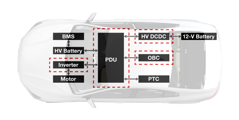
Figure 1: An overview of the typical architecture in an EV
Why is a powertrain integration great for HEV/EVs?
Integrating powertrain end-equipment components enables you to achieve:
- Improved power density.
- Increased reliability.
- Optimized cost.
- A simpler design and assembly, with the ability to standardize and modularize.
A High-Performance, Powertrain Integration Solution: The Key to EV Adoption
 Read the white paper |
Current applications on the market
There are many different ways to implement powertrain integration, but Figure 2 outlines four of the most common approaches (using an onboard charger and a high-voltage DC/DC integration as the example) to achieve high power density when combining the powertrain, control circuit and mechanics. The options are:
- Option No. 1 with independent systems; not as popular today as it was several years ago.
- Option No. 2 can be divided into two steps:
- Share the mechanical housing of the DC/DC converter and onboard charger, but split the independent cooling systems.
- Share both the housing and cooling system (the most common choice).
- Option No. 3 with control-stage integration is currently evolving to Option No. 4.
- No. 4 has the best cost advantage because there are fewer power switches and magnetic components in the power circuit, but it also has the most complex control algorithm.
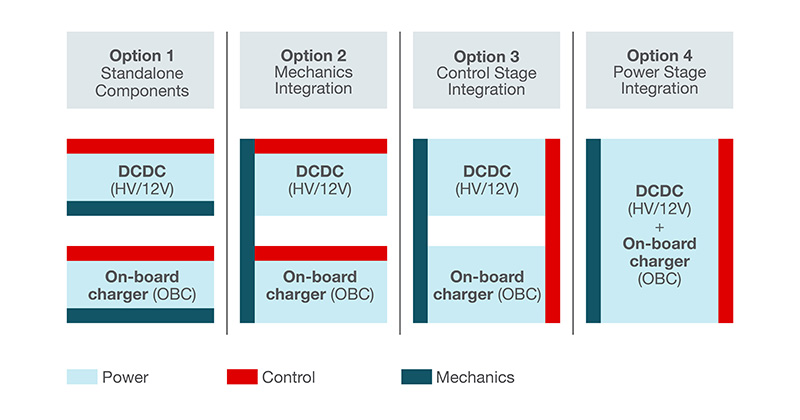
Figure 2: Four of the most common options for a OBC and DC/DC integration
Table 1 outlines integrated architectures on the market today.
High-voltage three-in-one integration of OBC, high-voltage DC/DC and PDU optimizing electromagnetic interference (EMI) | Integrated architecture integrating an onboard charger plus a high-voltage DC/DC converter | 43-kW charger design integrating an onboard charger plus a traction inverter plus a traction motor (option No. 4) |
*Third party data reports that designs such as this can achieve approximately a |
(one microcontroller [MCU] control power factor correction stage, one MCU control DC/DC stage and one high-voltage DC/DC) |
|
Table 1: Three successful implementations of powertrain integration
Block diagrams for powertrain integration
Figure 3 depicts a powertrain block diagram implementing an architecture with power-switch sharing and magnetic integration.
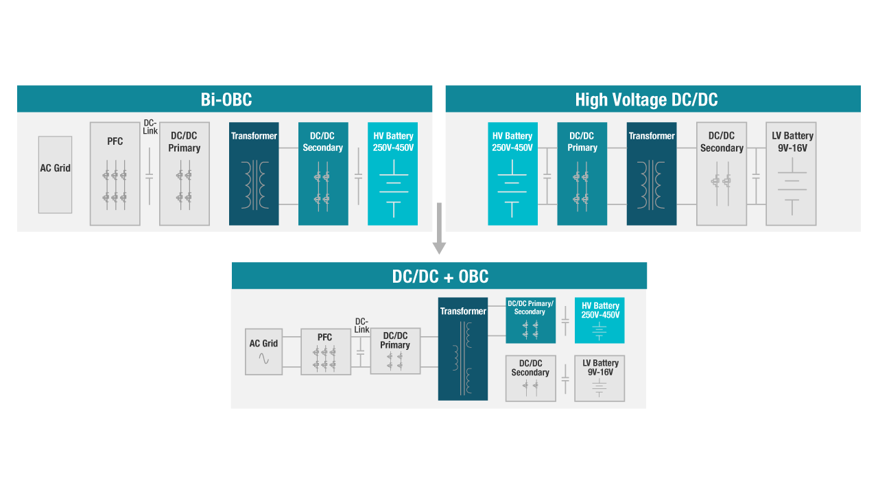
Figure 3: Power switch and magnetic sharing in a integrated architecture
As shown in Figure 3, both the OBC and high-voltage DC/DC converter are connected to the high-voltage battery, so the rated voltage of the full bridge is the same for the onboard charger and the high-voltage DC/DC. This enables power-switch sharing with the full bridge for both the onboard charger and the high-voltage DC/DC.
Additionally, integrating the two transformers shown in Figure 3 achieves magnetic integration. This is possible because they have the same rated voltage at the high-voltage side, which can eventually become a three-terminal transformer.
Boosting performance
Figure 4 shows how to build in a buck converter to help improve the performance of the low-voltage output.

Figure 4: Improving the performance of the low-voltage output
When this integrated topology is working in the high-voltage battery-charging condition, the high-voltage output will be controlled accurately. However, the performance of the low-voltage output will be limited, since the two terminals of the transformer are coupled together. A simple method to improve the low-voltage output performance is to add a built-in step-down converter. The trade-off, however, is the additional cost.
Sharing components
Like the OBC and high-voltage DC/DC integration, the voltage rating of the power factor correction stage in the onboard charger and the three half bridges is very close. This allows power-switch sharing with the three half bridges shared by the two end-equipment components, as shown in Figure 5, which can reduce cost and improve power density.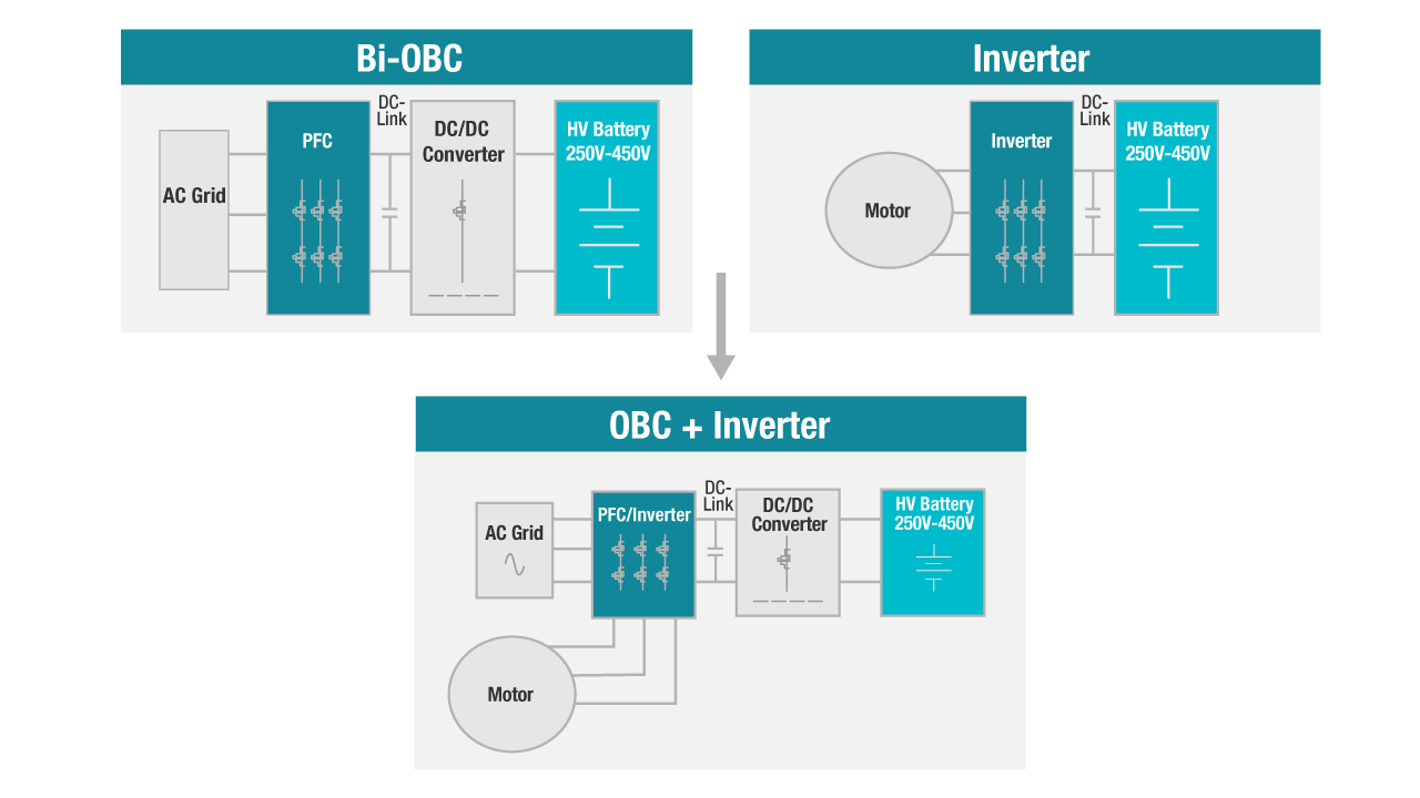
Figure 5: Sharing components in a powertrain integration design
Since there are normally three windings in a motor, it is also possible to achieve magnetic integration by sharing the windings as the power factor corrector inductors in the OBC which also lends to the cost reduction and power-density improvement of this design.
Conclusion
The integration evolution continues, from low-level mechanical integration to high-level electronic integration. System complexity will increase as the integration level increases. However, each architecture variant presents different design challenges, including:
- The need for careful design of the magnetic integration in order to achieve the best performance.
- The control algorithm will be more complex with an integrated system.
- Designing the high-efficient cooling system to dissipate all of the heat within smaller systems.
Flexibility is key with powertrain integration. With so many options, you can explore this design at any level.
Additional resources
- 98.6% Efficiency, 6.6-kW Totem-Pole PFC Reference Design for HEV/EV Onboard Charger.
- Bidirectional CLLLC Resonant Dual Active Bridge (DAB) Reference Design for HEV/EV Onboard Charger.
↧
How smart amps are bringing high-fidelity audio into the smart home
Other Parts Discussed in Post: TAS2563

Smart speakers have become ubiquitous in homes, raising the bar for consumer audio quality standards in household items. New audio features are popping up in unlikely places: digital voice assistants in coffeemakers that announce a fresh brew, or digital thermostats that can tell you the weather while playing your favorite jazz album (Figure 1). As consumer reliance on smart home technology increases, previously strange situations such as having conversations with visitors through a video doorbell are becoming common.
As a result, many home electronics designers are either upgrading their audio subsystems or introducing audio to their circuits for the first time. As consumer audio quality demands increase, engineers face a new challenge: how to get louder, clearer and more powerful audio without compromising the form factor of the product with a larger speaker or battery. In this article, I’ll discuss how smart home product designers are increasingly using smart amps– Class-D amplifiers with integrated speaker protection and audio processing – to enable high-fidelity audio in space-constrained systems.

Figure 1: Audio is increasingly common in many modern household products
While technologies such as Bluetooth® Low Energy and mobile processors make smart home products possible, significant improvements in audio technology are making smart home interfaces more accessible. For example, the beeping of an oven that has finished preheating is driven by a traditional 5-V, 2-W Class-AB amplifier. These amplifiers don’t get louder than 2 W without introducing an uncomfortable amount of distortion (greater than 10% of total harmonic distortion plus noise). This standard of performance is fine for a simple beep or alarm, but most 5-V Class-AB amplifiers are hardly powerful or clear enough for the modern smart home experience. Smart amps are bridging the quality gap.
TI originally developed smart amps to overcome a challenge in smartphones – how to get their tiny speakers to sound loud and crisp without damaging the speakers or draining the battery. Built on top of a high-fidelity Class-D amplifier, TI’s smart amps use a current- and voltage-sense-based speaker protection algorithm to push speakers beyond their rated temperature and excursion limits – achieving louder volumes without damaging the speakers. Using a smart amp makes inexpensive, small-form-factor speakers sound much bigger than they are in space-constrained applications such as mini smart speakers and tablets.
Smart amps represent a minor revolution in audio technology, making it possible to forget the usual trade-offs between loudness, size and power efficiency, and instead achieve all three. As the technology has matured and the benefits have become more widely known, smart amps have started to become a key enabler in smart home products such as thermostats, security cameras and kitchen appliances.
In addition to loud, high-fidelity audio, smart amps provide other valuable features in smart home applications, such as two-way audio communication in a video doorbell. Implementing an effective voice interface or two-way functionality can get complicated. Analog microphones require digital conversion; echo reference data must be taken from the speaker and sent to an echo-cancellation algorithm on the processor, and the Class-D amplifier needs a voltage boost to provide more output power.
Using a smart amp simplifies the signal chain immensely. Figure 2 shows how the TAS2563, a TI smart amp with an integrated digital signal processor and Class-H boost converter, fits into a two-way audio system. The TAS2563 integrates much of the signal chain by sending digital microphone inputs and post-processed audio back to the host processor through the smart amp’s Inter IC-Sound (I2S) stream.
Traditional two-way audio system
| Two-way audio system with smart amp
|


Figure 2: Smart amps integrate most components of a two-way audio system in a single package
While smart amp development may seem complicated, TI is making it easier for any engineer to get the best audio performance from their product. TI software engineers have given PurePath Console 3, the graphical user interface for smart amps, a refresh. Newly streamlined tuning features such as voice and music presets make it easy to generate great sound quickly from a speaker, eliminating barriers to implementing high-quality audio in any application. TI audio engineers have released a series of training videos, application notes and FAQs to help you add high-quality audio to your smart home, building security or small appliance project. The TAS2563 is the also first smart amp available in quad flat no-lead packaging to accommodate more manufacturing flows.
Smart amps have already proven to be a powerful yet surprisingly easy-to-learn component in any end-to-end audio solution. With the large output power range of smart amps and the support available, it’s a good time to experiment with the sonic possibilities, even in applications that don’t currently take advantage of audio features. By capitalizing on advances in audio technology, it’s possible to find innovative ways to connect with smart home users.
Additional resources
- Check out this video doorbell reference diagram with two-way audio.
- Download the High-Fidelity, Near-Field Two-Way Audio Reference Design with Noise Reduction and Echo Cancellation.
- Read the technical article, “Get Started with Smart Home Audio Design.”
↧
↧
Bulk up your 24-VDC power distribution with industrial high-side switches
For athletes to perform at their highest level – to run a mile in less than five minutes or leap into the air and dunk a basketball – they need strong muscles. The heart supplies blood through the veins to the muscles to enable movements such as gripping an object with your hand or moving a finger when your brain instructs it to. But without muscles, these spectacular feats would not possible.
Similarly, factory floors use a 24-VDC power network to distribute power from power supplies (the heart) through wires and connectors (the veins) to different power switches (the muscles), enabling the movement of relays, actuators and sensors when the programmable logic controller (the brain) tells them to do so. This is evident in large machine tools that use power switches to internally transfer 24 V of power – from board to board, or externally in digital output and remote input/output modules – to distribute power to relays, actuators and sensors. These power switches enable robots, motor drives and other large machine tools to automate a factory to perform tasks at a high speed and with precision – much like the athletes we love to watch. Figure 1 is a visual representation of a factory illustrating the use of power switches in different types of factory automation equipment.

Figure 1: Illustration of power switches in different factory automation equipment
So what type of semiconductor devices act as the muscles in a factory environment? Industrial high-side switches from TI go beyond just distributing power and drive output loads – they also provide protection and diagnostic capabilities to prevent extended factory downtimes. For example, the switches include features such as:
- Adjustable current limiting for short-circuit and overload conditions.
- Integrated current sensing for load diagnostics, thus reducing downtime.
- Open-load detection for wire breaks.
- An integrated drain-to-source voltage (VDS) clamp for inductive load driving.
One of the most important protections is current limiting, which helps keep factory automation systems with board-to-board connections and offboard loads from experiencing significant downtime due to short-circuits, which could be caused by condensation/humidity, wire breaks or short-to-ground scenarios. TI’s high-side switches also have the option for an external resistor to adjust the current limit, offering added flexibility. This flexibility makes it possible to use the same switch across a variety of output load conditions. There is no need to buy an additional device; simply change an external resistor to get a new current-limit value. Figure 2 is a block diagram of a dual-channel high-side switch with independent adjustable current limits for each of its output channels.

Figure 2: Dual-channel high-side switch, TPS272C45
Integrated current sensing offers the ability to sense the amount of current flowing through the high-side switch, which can be invaluable when debugging a machine that’s not working properly.
The switches output a current onto an external resistor that is proportional to the current passing through the internal power metal-oxide semiconductor field-effect transistor, which can then be fed to an analog-to-digital converter (ADC) in the system for processing.
Current sensing enables users to diagnose open-load situations if a wire were to break or become unplugged in a machine. This can greatly reduce debugging time for large machines that have many outputs or board-to-board connections by enabling technicians to better pinpoint which system may have the broken or missing wire, and get the system up and running again.
Additionally, current sensing can help determine whether a system is experiencing an overcurrent event or drawing an unexpected amount of current. This can alert technicians to bring a spare load or subsystem to replace the faulty one.
Providing feedback to the system that a certain load has turned on correctly is another benefit of current sensing. There are loads, such as a solenoid actuator, which have a very distinct input current profile. A typical current profile for a solenoid actuator is shown in Figure 3 below and has three components to it; a stall current, a notch current and a holding current. This profile can be captured by the high-side switches current sensing and sent to an ADC for analysis. This analysis can help to provide a feedback mechanism to the system, indicating that the load it’s powering did indeed turn on correctly and the system is running as expected.

Figure 3: Output current profile of a solenoid actuator captured by current sense of TPS274160
TI industrial high-side switches not only provide more muscle power with low drain-to-source on-resistance RDS(ON) solutions; they also provide flexibility and intelligence in your factory systems to enable more reuse and less downtime. TI is continuing to build out its industrial high-side switch portfolio with lower RDS(ON) switches, more feature integration and higher channel counts.
Additional resources
- Review the following data sheets, which describe the capabilities of high-side switches for use in industrial applications:
- Review the following application reports, which describe the use of high-side switches in factory automation and motor drive systems:
↧
Understanding the importance of functional safety in automotive and industrial sensing applications
According to the U.S. Bureau of Labor Statistics, there were 2.8 million nonfatal workplace injuries in 2018. As design engineers, we often think about our world – or more specifically, the applications we develop – in binary code: 1s an...(read more)![]()
↧
How to maximize powertrain efficiency and reliability with high-accuracy temperature sensors
Other Parts Discussed in Post: TMP126-Q1
If you design automotive systems, you may feel tremendous pressure to redefine vehicle powertrain systems to meet the reduced greenhouse gas (GHG) emissions goals established by initiatives in the European Union, United States, China and Japan, just to name a few. To meet these targets, some automobile manufacturers are implementing 48-V systems for mild hybrid electric vehicles, but most are transitioning traditional internal combustion engine (ICE) models to an all-electric powertrain system, as shown in Figure 1.
Due to environmental goals for emission reduction, electric vehicles (EVs) are projected to quickly increase their market share over the next decade. To help speed the adoption of EVs, powertrain suppliers are designing integrated electric powertrains that include the traction inverter, DC/DC converter and onboard charger in one box. While this approach reduces vehicle weight, lowers overall costs and provides higher power density, it requires greater focus on thermal management. This is because higher power densities and smaller form factors increase operating temperature, which can degrade powertrain system performance – or even worse, damage it. Temperature sensors have always been a necessary component within vehicle powertrains, but because they’re often a second thought or reused across designs for years, their positive impact on electric powertrain systems has been limited. New temperature sensor technology with proper implementation can have a great impact on the efficiency and reliability of integrated electric powertrain systems.

Figure 1: Electric powertrain systems
Better temperature accuracy can help increase the efficiency of integrated electric powertrains
Consumers want EVs to charge more quickly and to have more driving range on a single charge. In order to achieve this, designers must increase the efficiency of the integrated electric powertrain. One approach is to increase the voltage levels and switching frequencies within the power stages. However, doing so in such a small footprint intensifies the power density and causes temperatures to rise, adding to the risk of thermal runaway. Achieving this increase in efficiency while limiting the risk of thermal damage requires the proper use of accurate temperature sensors and active cooling feedback loops.
Safely pushing components to their peak performance typically results in higher operating temperatures closer to device limits. As shown in Figure 2, maximizing sensor accuracy enables the processor to minimize the temperature safety margin of error so that it can more precisely control functions such as vehicle charging and power flow – even when close to the thermal operating limits of your devices.

Figure 2: How accuracy affects safety margins
Low-drift temperature sensors help maintain the reliability of integrated powertrain systems over time
Consumers want their vehicles to last. The lifetime of the electronics found in an integrated electric powertrain directly correlates to the temperatures at which they were exposed. In order to keep components such as the power-stage field-effect transistors operating correctly for many years, temperature sensors must be reliable and have minimal drift.
Many electronics drift over time, and temperature sensors are no exception. Drift has a lot to do with a sensor’s material composition. For example, silicon-based temperature sensors have negligible sensor drift over time, while resistance temperature detectors drift anywhere from ±0.1 to ±0.5°C per year, and traditional negative temperature coefficient (NTC) thermistors typically drift >5% over time (not including the drift of external components). As your system ages, sensor drift can increase the error of your temperature sensing solution and limit its efficiency by forcing it to shut down prematurely or cause thermal damage to components.
When designing for long-term performance, it’s best to use a temperature sensor integrated circuit (IC) that provides guaranteed accuracy over its full operating temperature range, as opposed to the questionable accuracy that discrete implementations such as NTC thermistors have when uncalibrated. A digital temperature sensor such as the TMP126-Q1 enables precise monitoring up to extremes as high as 175°C with ±1°C accuracy, and down to ±0.3°C across a wide temperature range. In the case of voltage transients and surges within the system, temperatures can increase pretty quickly.
As Figure 3 illustrates, the TMP126-Q1 helps your system take preemptive action by detecting temperature spikes, which may be a leading indicator of thermal issues before the temperature reaches dangerous levels.

Figure 3: The new slew-rate alert feature in the TMP126
As I mentioned previously, you might want to increase switching frequencies to boost efficiency, but that may lead to unwanted electromagnetic interference (EMI). To operate in high EMI conditions, the TMP126-Q1 has a built-in cyclic redundancy check to ensure the use of data only when it is error-free. Additionally, the TMP126-Q1 comes with functional safety failure-in-time (FIT) rate and failure mode distribution (FMD) documentation to help achieve system-level certification. The device’s high accuracy and negligible drift enable integrated powertrains to reduce their protection margins, shutting down less often while still protecting the system from overheating, leading to greater efficiency.
Conclusion
It’s not surprising that you can find over 20 temperature sensors spread across integrated electric powertrain systems. Accurate sensing can help maximize your system’s efficiency, prevent false triggering of control systems, and protect ICs or other components more effectively. Being able to maintain that efficiency over time to keep automobiles on the road longer is possible with low-drift sensors made out of silicon. No matter what temperature sensor you choose, remember to choose an accurate and reliable one, follow sensor placement best practices, and leverage new sensor features.
↧