Quantcast
Channel: TI E2E support forums
Viewing all 4543 articles
Browse latest View live

Core Wars (part 1)

$
0
0

I was recently invited to be the keynote speaker at a “Technology Day” event in Milwaukee, WI.  (If you have never attended one of these events, you should seriously consider it, as they provide an excellent venue for valuable interactive technology discussions between us and our customers.)    Seizing upon the opportunity, I chose to speak about a topic that is near and dear to my heart, and perhaps the greatest threat facing the microcontroller industry today.  I titled my speech “Will microcontrollers go the way of DRAMs?”  For those of us old enough to remember the DRAM saga, it was a fairy-tale story of a high-tech product with handsome margins and excellent growth potential.  But it didn’t end happily-ever-after, as DRAM margins began to erode, and the whole industry sank into the commodity space.  One by one, manufacturers dropped out when they realized they couldn’t use innovation as a competitive weapon, and the whole situation degenerated into all-out fab wars.  The problem was exacerbated when some unscrupulous DRAM manufacturers who were determined to own this market began dumping product below cost, thus hastening the inevitable end.

Could the microcontroller industry be headed toward a similar cataclysmic finale?  As George Santayana put it, “Those who cannot remember the past are condemned to repeat it.”  So, to understand where the microcontroller industry is going, we need to look at where it’s been.

The microcontroller had a quiet and humble nativity in the wee morning hours of July 4th, 1971, when Gary Boone and his team at Texas Instruments got their first prototype of a “computer on a chip” to work.  Unfortunately, TI underestimated the full potential of this breakthrough, and for a couple of years, the TMS1000 was used exclusively in TI calculators.  The microcontroller world would be a quite different place today had TI not waited until 1974 to make this chip available to the general market.  By then, Intel had already established a dominant foothold in this fledgling market.

The first fifteen years of the microcontroller age saw relatively few suppliers jump into the fray.  If you wanted to join this exclusive country-club of MCU players, you had to pay the hefty entry fees, and not many could afford the dues.  Several barriers to entry included:

1.  Expensive silicon foundry and fabrication facilities.

2.  The priesthood of silicon mages who understood how to design MCU cores was small indeed, and those who could wield this magic were well compensated.

3.  Unlike other semiconductor products that were pretty much stand-alone, additional resources were required to support an MCU family with assemblers, monitors, debuggers, development systems, etc.

Put all of these pieces together, and an image begins to form of a product with a huge appetite for development dollars which could only be satiated by big companies with deep pockets and/or well-endowed investors.

Now fast-forward to present day.  The microcontroller market has matured into a global presence representing estimated annual revenue of $18B in 2015, split amongst 40 or so suppliers.  What happened to cause this explosive proliferation?  Let’s take a look at three main events which changed the microcontroller world forever...

1.  Owning a silicon fab was a very prized, but very expensive proposition.  Operating margins were directly linked to your ability to keep your fab running all the time at full capacity.  As a result, many MCU manufacturers who owned fabs started renting out spare fab capacity in order to maintain a predictable backlog of silicon starts.  Related to this effect, third-party fabs began to spring up all around the globe.  Even many of the “big guys” started outsourcing some of their fab requirements to lighten their asset costs.  Suddenly the first barrier was down, and smaller companies now had access to fabs to manufacture their own MCU products.

2.  As the uC/uP market matured, the mystique of core design began to dissipate.  Mature players in this market were looking to recoup early R&D costs by licensing older core technologies (like the 8051) to the general market.  But perhaps the most devastating body-blow to the elitism of proprietary cores was delivered by a British company named Acorn Computers.  In the late 80s they developed a core which they called the “Acorn RISC Machine”, and began licensing it to other companies, including Apple and DEC.  In 1990, Acorn Computers spun-off the core design team into a new business called “Acorn RISC Machines, Ltd”, or simply “ARM” for short.  Now, a non-proprietary core with an upwardly mobile migration path was generally available for a relatively small licensing fee.  This concept caught on like wildfire, and by 2005, 98% of all mobile phones contained at least one ARM processor.  The second barrier came down with a resounding “thud” that could be heard around the world.

3.  Even with the first two barriers down, playing in the MCU space was still an expensive proposition due to the huge overhead burden required for support products and services.  But it was inevitable that as the MCU industry matured, third party support services began to pop up everywhere.  If you have ever been to Austin TX, you know exactly what I’m talking about.  Guys on street corners carried cardboard signs that read “Will test silicon for food”.  Neon signs glowed softly in the night…“Bubba’s Barbecue and peripheral design services”.  (OK, maybe I’m exaggerating a little, but you get my point.)  At the end of the 90’s, I recall a conversation I had with a division manager for the semiconductor company I worked for at the time.  To paraphrase, he said, “Just about everything we do here can be outsourced.  With my connections, I’m sure I could start my own MCU company if I wanted to, and just outsource everything.  And if I can do it, I’m sure there’s a whole bunch of other people around here who can do it too!”  As I left his office that afternoon, I finally realized that all the barriers were down, and the MCU industry was turning into the Wild West.

In the next part of this blog, I will discuss the strategies taken by some of the entrenched MCU suppliers to remain competitive in the face of almost certain commoditization.


Crossing the Rubicon with new WEBENCH PCB Export

$
0
0

Imagine this:  You are driving along a highway which is fantastically beautiful and a memorable ride, but reach a scenic point and realize that you are at the end of the road.  Maybe there is a beautiful mountain, the ocean or a river in your way. A sign at the dead-end reads “Thanks for enjoying our highway.  Best wishes on your future travels.”  You can see fantastic scenery across the way, but wonder how to get there. “How am I going to cross this leg of my journey?”

There could be lots of options — maybe continue through a tunnel drilled through a seemingly impenetrable mountain, or cross the ocean aboard an aircraft carrier, or drive over the Rubicon River on a majestic bridge.

This is akin to the barrier we broke today with the release of WEBENCH PCB Export.

Those of us who are familiar with TI’s WEBENCH Power Designer know the drill:

  • Enter power system specifications into WEBENCH

  • Moments later, your design is ready

While just a click or two for the designer, this is a momentous and non-trivial task, which Power Designer makes easy with its smart but complex algorithms.

But there is still work to be done.  At this point, the designer needs a physical realization of his design. Quite honestly, he needs the design to jump off of the screen to his physical bench and power his system.  This was the mountain/ocean/river that we have been working hard to cross. He needs WEBENCH to cross the Rubicon.

And now it does!

After years of work, we have developed a new tool that exports—literally hands it to the user—the PCB layout. This layout, generated by WEBENCH PCB Export, uses intelligent algorithms to incorporate all the specifics of your design, prepares the PCB layout and then exports it into the format of your favorite CAD tool, includingAltium Designer, Cadence Allegro, CadSoft EAGLE, Mentor Graphics PADS and DesignSpark PCB. The design you started in WEBENCH can now be driven all the way into your CAD software.

So start a design now in WEBENCH Power Designer and try the new WEBENCH PCB Export feature to get yourself across the Rubicon. Come back here to share your experience using it - I'd love to hear how it works for you.

For those of you visual folks, please watch the video on PCB Export by Jeff Perry, director of our WEBENCH Design Center.

College students bike across America to get kids excited about engineering

$
0
0

Emma Benjaminson did not have a lot of exposure to engineering as a child. Her parents were both civil servants, so most of her knowledge of the work of an engineer came from the hit TV show “Star Trek: The Next Generation.”

“Geordi La Forge [chief engineer of the USS Enterprise] was my idol. I just wanted to be the person who could walk into a star ship and turn it on, get it to work and fix everything,” said Emma.

While Emma only had “Star Trek,” the students she expects to find along her more than two month biking tour across the United States as part of Spokes America will have the opportunity to actually meet and learn from real-life engineers. Emma and six other college engineering students from MIT, Harvard and Columbia University will spend time with students who live in rural or low-income areas. This is the second year college students have taken part in Spokes America, with the goal of sharing the enthusiasm they have for science, technology, engineering and math (STEM) and encourage self-driven, curious and creative learning. At each of the 10 stops, the engineering students will conduct hands-on workshops with middle and high schoolers in the hopes of inspiring the students to take something apart, read about what interests them and experiment until they make a new discovery.

“We are really trying to give them the tools to change their attitudes in such a way that they believe they can solve any problems they encounter,” said Emma.

Each of the seven college students will teach a different workshop. For example, one hour will be spent playing math games, while the next will involve students taking apart different parts of a bike to see how they work, followed by an hour of manufacturing simulation with LEGOs to learn manufacturing techniques. TI has donated BeagleBone Blacks and MSP430 LaunchPads for a workshop about basic computer coding concepts.

“We’re engaging the students to encourage them to be more curious about computer science and engineering, and we’re giving them different critical thinking tools that they can use to think about STEM subjects with confidence,” said Emma.

The seven college students could have driven, taken the train or flown from one city to the next on their education tour – so why bike across the country? For Emma, it’s about how scientists and engineers are perceived in the U.S. She wants students to see them as more than just socially awkward sitcom characters but as real people who are athletic, passionate and interesting. TI sees all of the elements of the bike tour as essential to getting the youth of America interested in STEM careers.

“This program was important for us to sponsor because it brings together three areas that we at TI care a lot about – health & fitness, education and of course engineering innovation,” said Steve Lyle, director of TI university marketing and engineering workforce development. “The fact that these university students care that much about educating the next generation to help them understand how to quickly apply their knowledge is inspiring to me. They are giving their time and a lot of energy to this and I could not be more proud of them.”

“We’re very grateful that TI thinks what we are doing is valuable and there willing to support us. TI is helping the kids who we reach out to, but they are also helping the six people that I am biking with, giving us the confidence to believe that we can do crazy trips like this,” said Emma. “I think TI is creating seven new engineering leaders who are not going to stop here. We’re going to go on and do other, great things.”

And maybe they’ll connect with a kid on their biking trip who will become the next crew member on the USS Enterprise, or even better, the next Spokes America team member.

Connected gateways for the IoT – ZigBee Home Automation

$
0
0

By Oded Amihai and Saurabh Narang

Within the Internet of Things (IoT), the majority of wirelessly connected devices need that extra help actually connecting to the Internet. True, there are Wi-Fi enabled devices that can connect directly to the cloud. There are Bluetooth- and Bluetooth low energy-based applications that can connect to the Internet via an existing central device, like a smartphone, tablet or PC. However, the vast majority of IoT devices need a specialized gateway to access a provider’s network and be accessible from the web. For example, to connect an IoT node that uses ZigBee or Sub-1 GHz / 6LoWPAN to the Internet, you need a gateway that supports the respective protocol and also provides either Wi-Fi or Ethernet connectivity.

Gateways come with a wide range of connectivity options and features, depending on the actual requirements – for example, a home gateway may not need as many connectivity methods as an industrial gateway. In this series we will introduce different gateway architectures and reference designs available to speed development. First up is a ZigBee home automation gateway.

As a major player in the home automation field today, ZigBee is being used to connect many types of devices including lighting systems, security and alarm systems, home appliances and more. There are many reasons why ZigBee is a good choice for home automation. Based on a mesh network topology, ZigBee offers an extended range compared to other technologies such as Wi-Fi and Bluetooth, and delivers a self-healing network that can expand to hundreds of nodes. While connecting many devices in the automated home, ZigBee maintains backup routes that can be used if one or more nodes fail. Additionally, ZigBee provides an application-level standard that guarantees product interoperability – this is demonstrated in practice by the many interoperable ZigBee devices that already exist in the market. Another important quality of ZigBee is that it is a low-power technology – ZigBee devices can support operation on a single coin-cell battery for a considerably long duration.

As noted above, ZigBee devices need a gateway in order to connect to the cloud and provide remote access, so consumers may control their home devices away from home (e.g. from a smartphone or tablet). TI recently released a new ZigBee home automation gateway TI Design, that combines the SimpleLink™ ZigBee CC2531EMK with the Sitara™ AM335x processor-powered BeagleBone Black. This is a ZigBee plus Ethernet connectivity solution on an open-source Linux platform. It provides a ZigBee to IP bridge that offers easy subsystem integration at the TCP level and enables a wired or wireless IP link, which is perfect for full home and building automation applications. Additionally, this scalable and flexible Linux integration of ZigBee allows porting to other gateway hardware platforms and enables versatile application development.

This TI Design makes it easy to get started building your own ZigBee home automation gateway by providing Gerber files, layout, schematics, block diagrams and BOM references. Also included is a complete and scalable Linux-based software solution, leveraging TI’s Z-Stack™ software. This design is first of its kind, allowing you to easily integrate ZigBee technology into a gateway. With tens of APIs, it dramatically simplifies hundreds of commands and protocol operations that would have otherwise be required in the integration of a ZigBee subsystem. Plus, the design is a plug-and-play ZigBee solution that includes ZigBee Home Automation HA1.2 certified Protocol Stack, MAC and PHY, and is extensively tested for interoperability.

The Sitara AM335x processor that powers the BeagleBone Black provides 1 GHz performance, enabling support for advanced user interfaces and offers extra computation power. With all components on the board commercially available, including TI’s Sitara AM335x processor as well as several TI analog and mixed signal devices, users can quickly go from prototyping to kick-starting and take their devices to full production.

The ZigBee CC2531EMK USB dongle, built around the SimpleLink ZigBee CC2531 wireless MCU, is the other main part of the ZigBee home automation gateway design. This ZigBee dongle uses TPS76933 ultra-low power low dropout line regulator for achieving excellent power efficiency.

Get started by downloading this TI Design today!

The Empires Strike Back (part 2)

$
0
0


With more and more MCU suppliers pouring onto the battlefield, the entrenched players found themselves under siege.  Would MCUs be forced to surrender to the same fate that DRAMs did years earlier in the commodity wars?  With so much at stake, MCU suppliers were determined to not let this happen to them, and to not take this onslaught lying down.  After all, they still represented the dreadnoughts of the industry with big guns and even bigger R&D budgets.  Smaller MCU companies instinctively knew not to engage this fleet head-on, or be obliterated.  But they were becoming more successful and more emboldened at outflanking the bigger MCU battleships in the niche corners of the market where agility was more important than sheer firepower.  As a result, several strategies were initiated by the established MCU players to keep them ahead of the pack:


1.  Powerful New Cores:  To prove that the concept of the proprietary core was not dead, and to combat the plethora of different cores that were flooding the market, established MCU players developed application specific cores designed to excel at certain types of calculations.  Perhaps the most notable example of this is the C2000 core from Texas Instruments.  With its Harvard architecture, single-cycle multiply-accumulate capability, and new vector math instructions, it is a perfect fit for real-time control applications such as digital power, motor control, closed-loop control, etc.  Once a core has proliferated to the extent that the C2000 has, it starts to take on a life of its own, and becomes very difficult to uproot as an incumbent choice for new designs.


2.  Continuous fab process innovation:  Unlike power semiconductor products where price is dictated by how many acres of silicon are required to support a given power level, MCU costs are heavily impacted by Moore’s law, which eats away at revenues every year like a cancer from the inside out.  Last year Intel demonstrated a laptop containing a processor built using 14 nm geometries.  The semiconductor industry is forecasting 10 nm geometries for 2016, 7 nm for 2018, and 5 nm by 2020!  As geometries shrink, so do the prices, which is undeniably a good thing for the consumer.  But does shrinking fab geometries translate into a sustainable competitive advantage for the manufacturer?  This question is particularly relevant when you consider that many third-party fabs offer geometry capabilities that rival the proprietary fabs.  It’s kind of like steroids.  As long as you are the only one taking them, you have a competitive advantage.  But when everyone is taking them, it levels the playing field again.  While remaining engaged in the fab war is important, it does not represent a sustainable competitive solution.  If DRAMs have taught us nothing else, it should be that shrinking the geometry only provides a temporary “fix” to keep you ahead of your competitors.


 3.  Innovative New Peripherals:  Older MCUs were considered innovative if they simply incorporated the uP core with some memory, and maybe some GPIO.  But today’s powerful MCUs incorporate everything but the kitchen sink!  Reaching out into the system to gobble up support silicon and auxiliary functions is a common strategy for MCU designers.  But in order for this strategy to work effectively, you must have broad shoulders to support a large family of MCUs, since the integrated peripherals you need are different for different applications.  As a result, this strategy works well for larger MCU companies who can afford to do this.

Not only are there more peripherals, but the peripherals are becoming more powerful.  In some cases, the peripherals themselves contain independent processor cores, like the Control Law Accelerator (CLA) from TI.  For much of my career I designed MCU peripherals for the motor control industry.  I was convinced that the best way to establish a distinct competitive advantage was to add unique features to these peripherals.  But I was quickly disillusioned when I realized how short this distinction lasted before someone else had the same or comparable feature.  And if you patented your improvement, all it did in many cases was broadcast your idea so that competitors could develop a work-around solution with the same or similar functionality.  Don’t’ get me wrong…peripheral innovation is crucial, and I am very proud to work for a company that prizes its leadership position in peripheral development.  But as I look at the motor control MCU market, I am compelled to admit that the peripherals from different manufacturers are all very similar in their basic functions with only subtle differences.  Therefore, I would again argue that in and of itself, fancy peripherals are insufficient to keep MCU suppliers ahead of the competition.


But there is one more super-weapon yet to be unveiled which has the potential to keep MCU manufacturers out of the gaping jaws of commoditization for years to come.  It has already been deployed by various MCU companies with varying levels of success.  Can you guess what it is?  I will discuss this in my next and final blog on this topic.

Sun, fun and technology: TI technology heats up the summer

$
0
0

Summer. To most people who live in the United States the word brings to mind road trips with family and friends, summer vacations at the beach, fireworks, no school and hot temperatures. Here at TI we welcome this time of the year (minus the scorching heat) with open arms. We are pleased to kick-off a summer long series, “Summer Adventures,” to let everyone know how TI is powering all your summer adventures from camping trips to cook outs all the way to a cross-country trip. To kick things off, let’s get Behind the Wheel with the ADAS team and go on a road trip.


“It’s a smile, it’s a sip of wine, it’s family time, it’s summertime!” – modified lyrics from Kenny Chesney’s hit Summertime

 It is safe to say that it is officially summer time!  Memorial Day is the unofficial start of summer in US, and for many it is also the last day of school. Whether your plans include spending time with extended family, a summer job or a family trip to Disneyland, there will be a lot of time in the car for the whole family.

To everyone on the road this summer, the top priority is a safe driving experience (except for the kiddos which is to get there as fast as possible). TI’s Advance Driver Assistance Systems (ADAS) is enabling technologies to help make the drive more convenient and potentially safer. With offerings such as System-on-Chip (SoCs) for vision and radar processing, Safety TMS570x MCUs, FPDLink, Power Management ICs and Analog Signal Chain, TI is enabling comprehensive BOM for Automotive ADAS solutions.

Last October, we announced the TDA2x processor product line which offers unprecedented performance and integration at low power envelope. This has been made possible with the introduction of TI’s innovative Vision Acceleration Pac with up to four Embedded Vision Engine (EVEs) specifically designed for analytics processing needed for ADAS solutions. This will allow running up to eight algorithms in a reasonable power budget enabling next generation ADAS applications which can provide guidance to the driver and in some cases can steer the cars out of potential accidents.

When you are behind the wheel of a vehicle powered with these technologies from TI, you will feel more relaxed while driving with your family.

Buckle up, sit back and relax. With TI on your side, summer time will be more fun!  


Inductive Sensing: How to use a tiny 2mm PCB inductor as a sensor

$
0
0

Recently, a customer asked me if he could use a tiny PCB coil as the sensing element for the LDC1000 inductance-to-digital converter (LDC). The PCB coil had only three turns per PCB layer on a four-layer board and measured 2mm in diameter. By itself, the inductance of the PCB coil was too low to produce an LC tank, which oscillates with the LDC1000. Since the location of the sensor was highly space constrained, I recommended adding a fixed series inductor to solve his dilemma.

Inductance-to-digital converters use an external LC tank circuit as a sensing element, which is comprised of an inductor with a series parasitic resistance and a parallel capacitor, as shown in Figure 1.

Figure 1: The LC tank senses proximity of conductive targets

The range of tank oscillation frequency is limited by the drive strength of the inductance-to-digital converter output driver. To ensure stable oscillation of the LC tank, the LDC1000 requires a sensor oscillation frequency between 5kHz and 5MHz, while ensuring that the equivalent parallel resistance (RP) at resonance remains between 798Ω and 3.98MΩ. These boundary conditions can create scenarios where the impedance of the chosen sensor is insufficient to design a suitable LC tank oscillator. 

When I measured the three-turn, four-layer PCB inductor with a network analyzer, I found that the inductance at the maximum allowed an oscillation frequency of 5MHz is 150nH. At this frequency, I measured a series resistance of 0.54Ω.

The LC tank oscillation frequency is given by:


Therefore, a 6.8nF capacitor would be required to reduce the tank oscillation frequency to 5MHz. However, the equation for the equivalent parallel resistance at resonance:


shows that RP is only 40.8Ω, which is significantly less than the minimum 798Ω that the LDC1000 tank driver requires to ensure stable oscillation. No capacitor value can be added to the 150nH PCB coil to produce an LC tank that operates within the fsensor and RP boundary conditions of the LDC1000.

To overcome this, I added a fixed series inductor to the sensor inductor, as shown in Figure 2. The series inductor increases the sensor impedance without operating at an unsupported oscillation frequency. Suitable fixed series inductors include surface mount (SMD) inductors and multi-layer PCB coils. The series inductor should not act as a second sensor, so it is important to either physically isolate it from movable conductive materials in its proximity or use a shielded SMD inductor.

Note that resolution is impacted when you use a fixed series inductor, because only a portion of the combined inductance acts as a sensor (a good analogy is adding a DC offset to an AC signal). Therefore, you should keep the series inductor as small as possible while comfortably satisfying the boundary conditions of the LDC1000. This will produce the best possible resolution.

Figure 2: Adding a series inductor increases sensor impedance

I added a TDK MLZ1608E4R7M multi-layer inductor in an 0603 package, which has a nominal inductance of 4.7μH. The sensor inductor and the series fixed inductor showed a combined inductance measurement of 5.3μH at 5MHz and a combined series resistance of 6.4Ω.

To allow some margin, I added a 270pF tank capacitor to produce a 4.2MHz oscillation frequency. The equivalent parallel resistance at resonance of this LC tank is 3.1MΩ, well within the specified RP range of the LDC1000.

If your LDC design is space constrained and dictates use of a physically small sensor coil that has low inductance, or if you’re using a small spring as the sensing element, all you need to do is add a fixed series inductor. This will provide LC tank oscillation within the LDC boundary conditions.

Have a question about designing with an inductance-to-digital converter? Search for answers and get help in our Inductive Sensing forum.

Additional resources:


Return of the Code Magi (part 3)

$
0
0

In this series we have been discussing the challenges facing the microcontroller industry over the last few decades, and some of the steps taken by MCU companies to remain competitive in a market that is becoming more and more crowded.  Recently a few MCU manufacturers (including TI) have turned to software as a secret weapon to win this war.

While software is certainly no stranger to the MCU industry, it has until recently been relegated to a support role for the MCU itself.  For example, even though MCU compilers are sold as a separate product, they are intended to support the main money-making product, the MCU.  Reference design software is often free, and again designed to support silicon sales.  This subjugation is understandable considering that the MCU industry was born out of the silicon industry.  At TI for example, 96% of our revenue comes from the sale of silicon based products.  If that much of your revenue is linked to silicon, it is easy to develop a mindset that your product must therefore be silicon.  I would argue that this is not true.  In fact, I would argue that most companies today don’t understand the true nature of their product.  For example, if I were to ask you “what is your product?” what would you say?  I suppose you might respond by telling me what you manufacture.  But your real product is not what you manufacture, but what you sell.

(Are you confused yet?)

Simply put, your customer is buying a lot more from you than what you manufacture.  They are buying your reputation, your support, and most importantly, the unique set of skills, creativity, and IP brought to bear which breathes life into what you manufacture, thus making it unique.  So if you accept that definition, should MCU companies consider their product to be “fancy sand”, or something far far more?  At the last semiconductor company I worked for, I made the statement that “any MCU company who still thinks their product is silicon will be out of business within a decade”.  Needless to say, I wasn't the popular kid on campus anymore.  Despite being harsh and perhaps mildly overstated, this statement makes my point exactly.  I still believe the industry as a whole needs to embrace a broader mindset that silicon is just part of their product; and in many cases, just the wrapper for their product.

Which brings me back to software.  I believe that the surviving MCU companies of the next decade will recognize and embrace the importance of software as part of their product portfolio.  I am glad that TI management understands this very well, and is aggressively instituting this concept with products like InstaSPIN-FOCTM.  For those of you who are unfamiliar with InstaSPIN-FOC, it is a powerful sensorless field oriented control algorithm used in motor control applications which is instantiated in ROM on select C2000 based products.  It’s a win-win proposition that solves an industry problem for our customers at a fraction of the cost it would take them to develop a comparable solution.  PLUS it allows TI to field a value-added non-commodity solution to the market.  You can find more information about InstaSPIN-FOC below.

www.ti.com/instaspin-foc

Of course, embracing software as a product instead of a support mechanism comes with a unique set of challenges that require MCU manufacturers to change how they do business.  Here are a few examples…

1.  You can’t please all the people all the time.  This statement is doubly true when it comes to software.  Most engineers agree that C should be the language of choice for embedded software, but that’s pretty much where the agreement ends.  For InstaSPIN-FOC, TI has made a conscious decision to embrace an object-oriented approach which is documented in a 487 page User’s Manual.  The code that interfaces with InstaSPIN-FOC is contained in MotorWareTM, which is TI’s new suite of software modules which adhere to our object-oriented coding standard.  But despite our best attempts to make MotorWare as easy to use as possible, we still get complaints that our software is too complicated, or is too structured, or ________(fill in the blank).  We recognize the challenge that this presents, and are continuously updating our documentation with examples and tutorials to educate our customers, and make the software easier to use.

2.  Some customers don’t trust the “black-box” approach.  As one who has a hard time trusting software tools and plug-in libraries, I can identify with this concern.  This has come up from time to time with InstaSPIN-FOC, but the number of instances I personally know of where we couldn't resolve this problem can be counted on one hand.  In many cases we can diffuse this issue by pointing out that if they are using our API libraries or IQ math routines (which are in ROM), then they have already been using a black-box approach.

This also means that whatever portions of your algorithm you chose to put in ROM must absolutely be tested through and through, because bugs in ROM code just confirm the black-box fears.  So far we have been very pleased with how robust and error-free the InstaSPIN-FOC ROM code has been.

3.  Some customers feel threatened by this approach.  When I sat down after delivering this speech in Milwaukee, I was immediately approached by an engineer who worked for a drives company who expressed this exact sentiment.  These customers typically fall into one of two categories:

a.  Engineers who feel you are doing THEIR job.  These are mostly software engineers responsible for writing the product code itself.  This can be a real problem, especially if their concerns are legitimate.  The last thing you want to do is alienate the very customers you are trying to help!  With InstaSPIN-FOC, engineers need to realize that it is NOT a complete motor drive solution.  Each module is designed to make your job easier, not replaceable.  Also, the structure of these modules is designed to allow you to use just as much or as little of the functionality as you want.

b.  Companies who worry that you are entering THEIR market.   For the case of TI and InstaSPIN-FOC, this is very easy to address.  I can unequivocally state that TI has no intention to enter the motor drives business.  We don’t have the expertise to navigate the complexities of this market, and would just as soon leave that to you, our customers.  We are content to offer pieces of the motor drive solution, but let our customers put them together.

4.  Marketing Approach.  MCU suppliers will need to be more flexible and adaptive with their marketing strategies.  For example, we have seen that certain segments of the market (like appliances, automotive, medical, hobby, etc.) have embraced InstaSPIN-FOC much more enthusiastically than we could have ever imagined!  But conversely, there has been less interest than expected from other segments, such as Industrial Drives.  This actually makes sense when you think about it.  The motor drives industry has already invested years of R&D to develop their own proprietary sensorless observers that are perhaps as good as (or maybe even better than) InstaSPIN-FOC in some cases.  So we have had to adapt our marketing tactics to serve our customers when and where it makes the most sense.

5.  Applications Support.  Finally, we have had to shift our applications support model from one that was almost exclusively silicon oriented, to one which also includes end application and software expertise.  This doesn't mean that we are reducing our hardware support capabilities, but it does mean that more software resources are being added.

__________________________

In conclusion, will MCUs go the way of DRAMS?  How do we as an industry keep from being sucked into the commodity black hole?

Should we continue to improve our fab processes?  Of course!

Should we integrate more peripherals?  Absolutely!

Should we continue to make our peripherals more powerful?  Again, the answer is yes.  But I am concerned that these actions alone do not represent a sustainable competitive strategy.  Unless we as an industry take bold steps to change how we perceive our products, I fear that we are in constant danger of becoming commoditized.

TI has shown the way for MCU manufacturers to remain relevant in this highly competitive market by providing high value-added solutions to our customers in the form of applications software running on powerful, control-oriented cores.


Improve backlight efficiency in portable displays

$
0
0

Battery life...oh, where did you go? Ever ask yourself that question at 3 p.m., and wonder how it gets so low so fast? When you look at today’s smartphones, or phablets (as they are sometimes called) and you see that the screens are getting bigger and bigger, do you realize that the display is what is taking up most of the power in the system?  

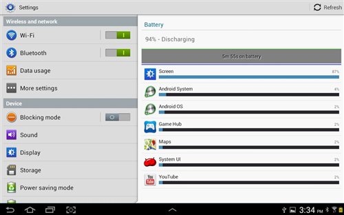
Take a look at this screen shot of a Galaxy Tablet running the Android operating system…  

Clearly you can see that the screen is what takes up the most power. Minimizing the power required for that part of the system directly impacts the battery life. Now, if you have kids, they have probably showed you that dimming your screen will make it last longer. But what if you are in the bright sun all day and need the brightness?

Choosing the right backlight device and the right configuration can make all the difference. TI’s LM3697 allows the designer to use 1, 2, or 3 strings to configure the LEDs for the backlight of the display. The more strings you can use, the lower the boost voltage, and the better the efficiency. In this simple example, you can see the impact of using 2 strings to drive 8 LEDs instead on 1.

On average, you can save up to 4% of the power used in the display, just by changing the configuration of the LED strings. Using the LM3697’s flexibility of having up to 3 strings for backlight connections, allows designers to choose the right configuration to maximize their efficiency.

Additional Resources:

PowerLab Notes: Powering the IoT in Our Homes

$
0
0

The internet of things (IoT) is already here. There has been a lot of buzz lately about the IoT and speculation about how it will shape our lives in the near future. Learn the uniqu requirements of your power supply with these connected devices.

The Internet of Things (IoT) is already here.  There is a lot of buzz lately about the IoT and speculation about how it will shape our lives in the near future.  While we have much further to go, look around your home and you will realize that we began this journey years ago. 

In order to understand how the IoT has already impacted your life, you must first get a general idea of what the IoT refers to.  What is the IoT?  It is basically the trend of devices and appliances (“things”) connecting to the internet to allow additional functionality such as control, transfer of data, etc.  For a more detailed description of the IoT, read about it here.

What examples of IoT connected devices can you find in your home? 

One of the more obvious “things” that has joined the IoT, is our home thermostats, fire alarms, and carbon monoxide detectors.  The Nest smart thermostat has been widely popular and has sparked many similar competing products. 

On the outside wall of your home is another example.  Smart power meters have been deployed by the utility companies for many years.  This saves money by eliminating the need for a human to travel around reading meters, and collects valuable information about energy usage over time.

With a trip to your local home improvement store you could buy products that allow you to connect much more of your home to the IoT.  Smart outlets, light bulbs, and light switches are available now that allow home owners to track and control their energy usage room-by-room, or outlet-by-outlet.

Although some IoT devices are becoming common place, 4 less expected IoT devices in your home are smart meters, wall outlets, light bulbs and light switches. All require AC power.

So what does all of this have to do with switching power supplies?  All of our examples already have power available to them, but it is AC.  To power controls, sensors and microprocessors, we need a low-voltage, low-current AC/DC supply.  These supplies usually do not require safety isolation, as they are not typically user-accessible.  The supplies must be small; after all, nobody wants a giant power supply to power a tiny microprocessor circuit. So here are 11 PowerLab reference designs for AC/DC IoT devices in your home!

11PowerLab reference designs for AC/DC powered IoT devices.

When safety isolation is not required, low-power flyback supplies can offer a very small, efficient and cost-effective solution.  This is a good solution for applications that require functional isolation for sensing the AC  line current, e.g. power meters and smart outlets.  Here are some PowerLab examples of flyback supplies for powering home devices in the IoT:

 3 low-power flyback power supplies for when safety isolation is not required.

  • PMP8968– 230VAC Input, 5.5V/250mA Flyback Converter
  • PMP9059– 120VAC Input, 5V/200mA Flyback Converter With BJT Switch
  • PMP9235– 120VAC Input, 5V/250mA Flyback Converter With BJT Switch

For applications only in the North American market (120VAC), a SEPIC converter can also provide a compact solution:

4 compact SEPIC converter power supplies for applications in North America

  • PMP5298– SEPIC (5V@250mA) for Auxiliary Bias Supply
  • PMP5353– SEPIC and LDO (3.3V@40mA; 15V@2mA)
  • PMP5422– SEPIC (5V@250mA) for Auxiliary Bias Supply
  • PMP6711– 120VAC Input to 5V/1.25W Output, Ultra Compact Isolated SEPIC

It is also possible to create a high-voltage buck supply:

  • PMP9087– Universal AC-DC Buck converter using UCC28710
  • PMP9176– Ultra Wide Input Voltage Range AC-DC Buck Converter using UCC28910

Another option traditionally used in power meters is the cap-drop method.  This method feeds a low-voltage linear regulator or buck power supply through a series-connected capacitor.  The impedance of the capacitor at the line frequency limits the input current.  A minimum load current or zener clamp limits the voltage feeding the linear or switcher.  A major drawback for this approach is the fact that the required AC blocking capacitor can become physically large, especially for applications with a wide input range or slightly higher power levels.  Here are some examples of cap-drop supplies:

2 cap-drop power supplies for power meters

  • PMP9310– 3.3V Low-Cost Non-Isolated Offline Converter for Smart E-Meters
  • PMP9311– Cap-Drop Offline Power Supply for Standard-Compliant Feature-Rich E-Meters

While the IoT has already started to improve our lives at home, it will affect us in many more ways in the near future.  Our automobiles, retail and grocery stores, and work places are all becoming connected now.  What other areas of your life has the IoT touched?

Find all PowerLab Notes here.

The train is at the station, get on it!

$
0
0

We are at the beginning of June, and many of the students are into their summer break.  This also marks the beginning of the next cycle of the Texas Instruments Innovation Challenge - India Design Contest.  The TIIC - India Design Contest 2015 train is at the station. It will leave on 15th of August 2014, the last date for proposal submissions.

 Being in India, I grew up travelling by train, and have become very fond of these travels. Train journey is symbolic of many of the experiences in life. It is a combination of the journey and the destination.  While the destination is what we may care about, or most remember in our in future, many times the journey adds its influence on our lives in its own ways. It could be in terms of the learnings we gather, the people we meet or the memories it leaves behind. The TIIC - IDC contest is like a train journey with a few differences. When you get on it, you do not know which station you would get off at. You earn a ticket and get on the train, but where you get off is a result of the efforts you have put, and the applied abilities you demonstrate. But no matter where you get off, once you are on the train you are bound to have a rich experience and have takeaways that are bound to influence your technical future.

 One of the key goals of the TI University Program is to enhance the hands-on experiences of the student community. One of the many vehicles we use to enhance the Embedded System Design experience is TIIC.

 The many reasons students see for participation in the TIIC IDC ahead of the 2014 cycle are already written about in Call for Innovation - Part I and Call for Innovation – Part II by Dr. Ravikumar. All of these are still relevant and hold true for this year’s contest as well. Amongst the feedback we have taken from the participants of the TIIC - IADC 2014, we have learned that the takeaways from the journey no matter how far you go are immense, and worthy for everyone to get on the train.

 Getting on the Train!

  As a first step, make your commitment by registering at www.ti.com/tiic-india-proposal.

 Then you can put together your team, select the problem you want to address and identify the key factors related to the problem that need to be addressed for the solution to have highest impact. This will automatically identify the innovations you need to come up with. The next step is where you put your technical and creative skills to the test in coming up with an innovative proposal. Brainstorm amongst the team, how you can address the problem differently and better than existing solutions, conceptually validate the ideas, and get to a proposed design. 

 Once you have a proposed design, do the necessary technical due diligence required in putting together the circuitry, identifying the different electronics components from TI that you would choose for the different functions, creating the schematic, doing the necessary simulations and fine tuning the different  parameters.

 At this stage, you should have most of the pieces to put together the technical proposal.  Please refer to the Submission Template to go ahead and put together the proposal. Submit the proposal with all the technical details and other supporting documents required as part of the guidelines for the qualifying round using the registration you had done above.

 Submitting your proposal before 15th of August 2014 gets you on the train.

 What is New with the journey?

 As with everything, we see the need to evolve and look for continued improvements, to enhance the journey for the students. There is a subtle change in the name, to India Design Contest, to broaden the focus to embedded systems and not just analog. Also we will be going outside India for the first time, as we invite few select colleges from Sri Lanka to participate in the contest as well.

 To reflect that, TIIC is an opportunity for the students to demonstrate technical innovation in directly addressing a real world challenge, we have added additional guidelines in the proposal template. This is factored against the judging criteria for Market Analysis and Impact in the Qualifying round. We have added an additional phase at the end for the finalists to focus on converting the prototypes into a well-defined product.

 The teams clearing the Qualifying round and entering the Quarterfinals can now request up to $250 worth of free tools per project.

 Looking forward to seeing a lot of you on the train!

Stanford University creates video game controller using TI technology that can sense a player’s emotions

$
0
0

Any video gamer has been there before – palms are sweaty, heart is racing, suddenly you’re breathing just a little bit heavier as the action on the screen in front of you reaches a climactic moment. But what if your video game console could recognize these signs of emotion – and respond? With TI technology, what started as that simple question has turned into a full-fledged research project at Stanford University.

“The idea is to be able to build a game that is tunable, so you will be able to make the game more exciting if the player gets bored or tone it down for children if the parents are becoming concerned that they are getting a little too focused on the game,” said Corey McCall, a third year PhD student at Stanford University.

Just about a year ago, Corey started his research focusing on video game controllers held in the hands of players. He replaced the back of a controller with a custom 3D printed back and loaded it with TI technology that can measure heart rate, respiration rate and hand movement among other physiological parameters.

“Emotions start in the brain, but are expressed in the autonomic nervous system that affects other bodily systems. So when you get excited, you may take faster or deeper breaths, or your heart rate and blood pressure may increase,” said Corey.

Watch this video from Stanford University to find out more about the emotion sensing video game controller:

(Please visit the site to view this video)

Besides the technology the team used, like the AFE4400 integrated analog front end for heart rate monitors and low cost pulse oximeters, and the ADS1292 complete low power integrated analog front end for electrocardiogram (ECG) applications, TI worked with the Stanford team on the overall research.

“We had weekly calls for almost six months combining all of our experiences with circuit design for sensing biological signals, trying to get the first prototype ready for CES2014 tradeshow. The demonstration garnered the interest of quite a few potential smartphone and gaming device customers,” said Karthik Soundarapandian, segment manager for TI health and fitness.

The first generation prototype of the emotion sensing game controller is now complete. Corey and his team continue to work on perfecting the algorithms before bringing in 20-40 test subjects to take clinical grade measurements to fully understand how the body changes while playing a video game.

“This is very exploratory work not really done at this level and scale. We hope to provide better and more data to the research community,” said Corey.

 The potential implications of this technology extend far beyond video gaming. The same technology could be used for anything people operate, including a steering wheel, joystick or yoke, from cranes to airplanes. If a system can detect when a person operating heavy machinery is stressed, sleepy or sick, it might be able to respond in a way to prevent accidents and save lives.

“If you can measure a person’s vitals through those controls with no straps or probes and no change in work flow, there is huge potential,” said Greg Kovacs, Professor of Electrical Engineering at Stanford University. Corey is a student in Prof. Kovacs’ lab.

While the research is promising, emotion sensing game controllers are still a few years away from being in our hands – unless you’re Corey McCall.

“This is a fun project. You could get a Ph.D. and work on very complicated and theoretical projects that may not come to market for a very long time. Something like this is very interesting and can be applied to real world problems in the immediate future, within the next few years,” said Corey. “The technology is there. A prototype is on my desk. So that is very cool.”

His work has already grabbed the attention of many, including articles from the NY Times Bits Blog and PC Magazine.

A bone of contention: ENOB or effective resolution?

$
0
0

As you might know, both ENOB (“Effective Number of Bits”) and effective resolution are parameters that relate to an ADC’s resolution. Understanding how they differ, and deciding which one is more relevant, is a subject of much confusion and frequent debate among ADC users and Applications Engineers alike.

Which one do you think is more important?

The ADC’s number of bits of resolution (N) determines the ADC’s dynamic range (DR), which represents the range of input signal levels that the ADC can measure. Generally specified in [dB] units, DR is defined as:

 Note that since the RMS amplitude of a signal over a given time window depends on how the signal amplitude varies over that time window an ADC’s DR changes depending on input signal characteristics. For constant DC inputs over its full-scale range (FSR), an ideal N-bit ADC measures maximum and minimum RMS amplitudes of FSR and FSR/2N, respectively. Hence, the ADC’s DR is:

Similarly, for sinusoidal inputs with amplitudes varying over the ADC’s FSR, the ideal N-bit ADC measures a maximum RMS amplitude of (FSR/2)/√2. The minimum measurable RMS amplitude for a sinusoidal input is limited by quantization error, which approximates a saw-tooth wave with amplitude half LSB or FSR/2N+1. The RMS amplitude of a saw-tooth waveform of amplitude A is A/√3. Therefore, the DR of an ideal ADC for sinusoidal inputs is:

Real ADCs have errors that degrade DR. In fact, depending on input signal characteristics, the ADC output has different types of errors that dominate when the input signal approaches its minimum value.

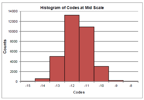
For constant DC inputs, the ADC's output error is dominated by so-called "transition" noise, which consists of the broadband thermal noise inherent to the ADC, its drivers, power supplies, and so on. If there are no gross linearity (DNL) issues with the ADC, transition noise produces an approximately Gaussian code distribution at the ADC output.

Figure 1: Histogram of ADC output codes for a constant DC input

One standard deviation (σHISTO) of this histogram corresponds to the RMS value of the transition noise. For σHISTO> 1 LSB, the ADC’s DC DR decreases to:

The decreased resolution or Effective Resolution can be recomputed by combining (2) and (4):

 Similarly, for time-varying inputs, the ADC's output contains dynamic errors, namely, quantization noise and distortion, in addition to transition noise that degrade DR. The altered DR is commonly known as SINAD, and the recomputed ADC resolution is known as ENOB. Therefore,

In summary, a given ADC can have different DRs and resolutions depending on whether the input is an AC or DC signal. Hence, there are separate metrics of ADC resolution that correspond to different input conditions – ENOB for AC inputs, Effective Resolution for DC inputs. Naturally, deciding which is more appropriate depends on your application. 

For an in depth look at optimizing the dynamic performance of your High Precision SAR ADC design, check out our webinar on EDN.


IEEE802.3bt: What’s your use case?

$
0
0

As I mentioned in my May meeting recap, an ad hoc was formed to collect use cases for 4-pair PoE.  Not only is this an important topic, but it gives me a chance to ask for some reader input again.  Regular readers of my posts know that in addition to keeping you up to date on the progress of the 4-pair task force, collecting your ideas so that I can bring them to the task force is the driving force behind my blog entries.  As such, I want to give some examples of use cases and ask for your feedback as to which of them you see end users implementing.  In addition, if there are use cases you are aware of that aren’t discussed here, please let me know.

The first set of use cases I want to discuss are the power level use cases

The most obvious use case of 4-pair PoE is the higher power applications it enables.  However, the highest volume applications that use PoE are those that use the least amount of power (4W or 7W loads), we don’t want to place an undue burden on these applications in the new standard.  In other words, we want to enable low power applications to use 4-pair PoE without increasing cost and complexity.  If you design or use PoE for low power applications, do you see yourself (or your customers) upgrading to 4-pair PoE if all that is required is a new switch or midspan?  What if a new switch and new powered devices (PDs) are required?  How about for slightly higher power applications (13W or 25W)?

The other set of use cases I want to discuss is powered devices that could use 4-pair PoE to power two independent loads inside a PD. In other words, the PD would present individual detection and classification signatures on each alternative to enable the switch or midspan to power them individually.  One example of this that I often hear cited is a security camera that would use separate power feeds for the camera and the motor/heater. 

I have also heard it suggested that a possible use case is to use two independent power feeds (one on each alternative) to provide redundant power to a PD.  In fact, the redundancy can be extended past the PD hot-swap FET to include independent DC-DC converters.  Can you see yourself or your customers building PDs with independent loads?  How about using redundant power feeds?

Power over ethernet (PoE) PD with two independent loads

Ok, one last request for your input.  Are there use cases that you know of that I didn’t discuss here?  What else should we be aware of when we are writing the new standard?  Please answer these questions and the ones throughout the post by commenting below.

PoE resources:

Challenges in high-speed communications

$
0
0

As many of you that work with high-speed signals may know… physics is not your friend – especially if you’re trying to design on lower-cost board materials, such as FR-4.  When moving data at 10 Gbps and above, all kinds of phenomenon – including dielectric loss; skin effect; transmission line impairments, such as connectors and ground plane stack discrepancies; and more – can affect channel performance.  All of these increase the jitter in the channel, ultimately degrading the bit error rate (BER).

Thankfully there are a few tricks to work around these issues. For example, you can use active devices to improve the signal transmission (improved amplitude as well as pre-emphasis or de-emphasis) or to equalize the channel at the receiving end.  Both have benefit, and in combination, can work around channel loss and various impairments.

When things get really bad due to non-deterministic jitter, you’ll need to use a re-timer (often called a re-clocker) to resample the data and produce a new, clean data stream. These devices can greatly improve signal quality and are often used just prior to optical modules where the jitter specification is extremely strict. So unless you’re one inch away from the source, you’ll probably need a re-timer.

Example re-timers include devices such as the DS100RT410, which includes the re-timer, receive equalizer and de-emphasis driver for a highly integrated solution for severe jitter conditions.  Also, if you’re like me and want to know in detail how a channel is operating, select a re-timer (like the DS100RT410) that includes an “eye-monitor” function built in. This allows you to read out the eye pattern directly from the re-timer to get a real-time image of the signal quality – it also helps tune the channel as well. Another trick is to move slower signals that are less than 5 Gbps utilizing careful layout techniques and then, when the signals need to be transported, further serialize them into a higher-speed stream. You can then transmit this stream via high-performance cables or by fiber via optical modules. 

At the other end, you can de-serialize the serialized data to reconstruct the original slower-speed serial links. To simplify this, you can use devices that contain two complete two-way channels that can run up to 10 Gbps, such as the dual-channel TLK10002 multi-rate transceiver (see Figure 1). By using one of these devices at each end, you can have two high-speed serial channels. This enables you to use one and have the second as a fail-over, or use them together to double the through-put.

Figure 1 – Using the TLK10002 to consolidate low speed connections can simplify signal integrity issues and box-to-box interconnections.

I hope this helps you with your next high speed interconnection challenge! Till next time…


Anywhere. Anything. Anyone: The new SimpleLink Wi-Fi family is here!

$
0
0

Today is an exciting day for our team and the wireless connectivity industry as a whole!  We introduced the next generation in our SimpleLink Wi-Fi family, the CC3100 and CC3200 Internet-on-a-chip™ platforms.  With this new family, we are offering two different flavors of Wi-Fi devices to help our embedded customers easily get to market quickly.  The CC3100 solution enables you to add Wi-Fi capability to any MCU. Even more, the CC3200 is the first programmable Wi-Fi MCU enabling true, integrated IoT development with just a single IC.  

Like never before you can easily add Wi-Fi and Internet connectivity to your products.  The new CC3100 and CC3200 solutions are designed for battery-operated products with the ability to run on two AA batteries for more than a year. We have enabled easy development for the IoT with flexible connection options, cloud support and on-chip Wi-Fi, Internet and robust security protocols. No prior Wi-Fi experience is needed to get connected.  These integrated protocols allow for easy implementation of IP applications such as service discovery, email, instant message and security.  All of these things are just a glimpse into the awesomeness of this product. So check out the below chart to get an in-depth view of what features and benefits the CC3100 and CC3200 have to offer: 

Wi-Fi can be anywhere. Now you can connect anything to the Internet. With the SimpleLink family, Wi-Fi is easy for anyone. Get started today: www.ti.com/simplelinkwifi

Free QNX Neutrino and QT full-day hands-on training on the AM335x Starter Kit. Register now.

$
0
0

TI training partner, ICS, is offering a free full-day workshop focusing on QNX Neutrino RTOS and QT. QNX Neutrino has been used in mission-critical applications, medical instruments, routers, air traffic control and more. Neutrino is specifically designed to work seamlessly with touchscreen user interfaces such as Qt. Combining QNX Neutrino with QT on an AM335x processor creates a beautiful real-time application.

In this hands-on workshop, you will create an animated touch-enabled application on the provided AM335x Starter Kit. Just bring your laptop!

For more information including training locations and to register, go to the TI Training page.


Alejandro Erives, Sitara ARM Processors Brand Manager.

Build it and they will come

$
0
0

Who would ever need 4.5 A of battery charging current? Who would ever have the space for 4-A power supplies in a smartphone? As they say, ‘build it and they will come.’ Consumers these days are demanding such feature-rich smartphones and tablets that electronics companies must build them. We power supply designers must work very hard to keep up and provide solutions that really pair with the increased power density requirements of the newest portable personal electronics.

The larger battery found in these systems is for both achieving a longer run time as well as providing higher peak powers, especially when processing power-hungry functions like streaming video and high definition video recording. These types of tasks put a huge strain on the battery, whose voltage drops due to its internal impedance and wiring in the system, as well as from simply having lower states of charge as these tasks are carried on. If the system designer is not careful, this input power source drop can cause the entire system to reset due to its input supply voltage being too low. A simple and straightforward solution to this dilemma is another power supply between the battery and system rail. But who has room and the power budget for another conversion step?

Enter the TPS63025x family to solve this dilemma. Packaged in a tiny 2.1 x 1.8 mm package, this buck-boost converter supplies 2A of output current to your system rail from battery voltages down to 2.7V. And it does it very efficiently—above 95% for most of the load range with over 90% efficiency at full load. With minimal impact to your solution size or power budget, who wouldn't want a 4-A power supply in their next smartphone?

Additional Resources:

Get Connected: SerDes interfaces

$
0
0

Welcome back to the Get Connected blog series here on Analog Wire! In the previous Get Connected blog post SerDes Demystified we examined the serializing and de-serializing of parallel data through devices known as SerDes. In this post, we will discuss how a SerDes makes up a smaller piece of another device known as a PHY, or physical layer device.

What is a PHY?

A PHY makes up the electrical connection between the data link layer (MAC) and the physical medium the data will be transmitted over. Figure 1 below shows a portion of the open systems interconnection (OSI) model. The OSI model is a conceptual model of the internal functions of a communications system. In this model, the MAC (media access control) interfaces with the PHY through the media independent interface or MII. A PHY will contain a physical coding sublayer (PCS), a physical media attach (PMA) layer, and a physical media dependent (PMD) layer. In the later versions of the IEEE802.3 standard, additional features like autonegotiation, link training, and forward error correction (FEC) were added but these are not required in every PHY device.

Figure 1: Open Systems Interconnection (OSI) Model

Sublayers explained

The physical coding sublayer or PCS allows the transfer of information to and from the MAC or other PCS clients like a repeater. The PCS performs frame delineation, encoding/de-coding such as 8b/10b or 64b/66b, fault information transport, deskew of received data, and data restoration.

The physical media attachment or PMA sublayer is responsible for local and remote loopback testing, PMA data framing, and test pattern generation (i.e. PRBS7 /CRPAT). The PMA layer is also where the rate per lane and the number of lanes is set. For example, some devices support multiple modes of operation and can be set up to run at 1x10Gbps, 2x5Gbps, or 4x2.5Gbps.

The physical media dependent or PMD sublayer is where the PHY interacts with the properties of the actual medium. The media can be a single or multimode optical fiber, CAT5 STP/UTP, backplane, or copper cable/wire. The PMD defines the details and standardizes the transmission and reception of the data stream on the medium.

Now that we’ve properly got your head spinning with acronyms, see the below image for a cheat sheet:

Difference between a SerDes, transceiver and PHY

We can now answer the question, what is the difference between a SerDes, transceiver, and PHY? A SerDes is a device like the SN65LV1023A – SN65LV1224B that simply serializes 10 bits of data with an added start stop bit for frame delineation. Transceivers and PHYs are in the same family of devices as they are made up of the same layers. What I have learned from my mentors that help develop early PHYs, is that the term transceiver was coined before the term PHY. This is why we have PHYs like the TLK2501 called transceivers. Figure 2 below shows the block diagram from the TLK2501 data sheet where the PCS, PMA, and PMD sublayers can be clearly observed:

Figure 2: TLK2501 1.5 to 2.5GBPS Transceiver


For more information on specific PHY application solutions, visit the High Speed Interface Forum in TI’s E2E™ Community and check out existing posts from engineers already using TI interface products, or create a new thread to address your specific application. 

Please join me for my next post in the Get Connected series where we will be discussing a XAUI to SFI application. If you are not connected you can get connected with one of the broadest Interface portfolio’s in the industry. 

Leave your comments in the section below if you’d like to hear more about anything mentioned in this post or if there is a topic you'd like to see us tackle in the future!  

And be sure to check out the full Get Connected series! 

TI creates new category of products to connect any device to Wi-Fi

$
0
0

On Monday, TI announced a new family of devices that are a big step toward creating a truly connected world.  Now that’s quite a big statement. But Amichai Ron, general manager of Embedded Connectivity Solutions (ECS) within TI’s Wireless Connectivity Solutions business, believes TI’s new invention will do just that.

 “We are releasing a new category of products that will allow you to add Wi-Fi to everything. It is completely different from the way people think of Wi-Fi today,” said Amichai. “Think back to 2007, before smartphones. And today, try to imagine your life without a smartphone. I think what we are introducing is the same thing in terms of the Internet of Things (IoT). In 5 years, many electronic devices will be connected to each other to make our lives easier. ”

Amichai will be the first to tell you that connected devices already exist today to a small degree, often only found in high-end products. He said the new SimpleLink™ Wi-Fi CC3100 and CC3200 platforms, which are about the size of a dime, will bring connectivity to everything from your toothbrush to your trash can. This family of products allows any piece of electronics to be connected via Wi-Fi because it uses very little power, doesn’t need an external microcontroller, can easily and quickly be connected to the cloud and most important – it reduces the system cost and complexity significantly.

Amichai sees the SimpleLink Wi-Fi family of products being used at three different levels. At its most basic level, washing machines, toothbrushes, weight scales, coffee machines, industrial equipment and more would be connected to the cloud through Wi-Fi. At a second level, such systems as the lighting in your home would become connected, creating the capability to turn lights on and off from your smartphone. But perhaps the most exciting level is the third one – where the devices themselves become intelligent and can communicate with each other through the IoT.

“Take a thermostat, for example, that can now make its own decisions. The thermostat can check the weather, and if it knows it is going to cool down in the afternoon and you are not at home, it can shut off the air conditioner. By the time you get to your house, it would be cool anyway,” said Amichai.

While power and cost has been one of the biggest hurdles to creating a truly connected world, another issue facing companies are the technical hurdles that must be overcome to create a device that is Wi-Fi enabled. For example, companies that make an irrigation system for watering backyards would have engineers with no experience with Wi-Fi. These companies, if they want to enable their products with Wi-Fi connectivity, would have to hire a team of engineers to figure out how to make those connections. Now, Amichai said even a recent college engineering graduate with a microcontroller (MCU) background can use chips from the SimpleLink Wi-Fi family.

“We call it SimpleLink for a reason – because it is very simple for the user that will eventually use the device, but it is also very simple for engineers to develop around it,” he said.

In fact, most Wi-Fi products on the market today require an MCU or microprocessor to run it, but the SimpleLink Wi-Fi CC3200 is the first product with an MCU built-in and specifically designed for this type of connectivity – it truly is the Internet on a chip™.  Another big difference with SimpleLink Wi-Fi: Amichai said other semiconductor companies are trying to modify Wi-Fi products designed for devices like smartphones and computers. TI invented the SimpleLink Wi-Fi family from the ground up with the intention of building a connected world.

“Our customers have started thinking about the possibilities. They are starting to innovate and think in a new way,” said Amichai. “I sometimes feel like we are inventing a whole new industry. Very few devices have connectivity. And everyone says we will have 25-50 billion connected devices by 2020. The SimpleLink Wi-Fi family is one of the big steps to enable IoT connectivity.”

Viewing all 4543 articles
Browse latest View live


<script src="https://jsc.adskeeper.com/r/s/rssing.com.1596347.js" async> </script>