Quantcast
Channel: TI E2E support forums
Viewing all 4543 articles
Browse latest View live

Get trained: SimpleLink Wi-Fi CC3100 and CC3200 family

$
0
0

With the recent introduction of the SimpleLink Wi-Fi CC3100 and CC3200 solutions on June 16th, TI is also hosting a multitude of trainings for you to learn about the features, benefits and application areas of these new tools and associated software. Our technical experts are traveling around the world and we want you to join us so we can help you start evaluating and get your projects kicked off.

If you can’t make it to one of the in-person training events, you can still get familiar with the CC3100 and CC3200 solutions through our free, on-demand training videos.

Register for trainings below to learn more about the CC3100 and CC3200 Internet-on-a-chip™ solutions and Connect more with TI!

To get started, order one of the follow kits:

Training

Date

Location

To register

Internet of Things Hands-on Development Workshop, Delhi

June 25th, 2014

Crowne Plaza-Okhla, Delhi, India

Register here

Building a Winning IoT Application by TI, Arrow and 2lemetry

Various dates from June to November 2014

Various locations through Argentina, Brazil and United States

Register here

TI MCU Design Days – Dallas, Texas

July 14th and 15th, 2014

Hyatt Regency North Dallas, Dallas, Texas, United States

Register here

TI MCU Design Days – Shenzhen, China

August 11th and 12th, 2014

Westin Shenzhen, Shenzhen, China

Registration opening soon!

TI Tech Days – Detroit, Michigan

September 12th, 2014

Venue TBD

Register here

TI MCU Design Days – Freising, Germany

September 22nd and 23rd, 2014

Munich Airport Marriot,

Freising, Germany

Registration opening soon!

TI Tech Days – Anaheim, California

October 14th, 2014

Venue TBD

Register here

TI Tech Days – Santa Barbara, California

October 15th, 2014

Venue TBD

Register here

TI Tech Days – Seattle, Washington

October 29th, 2014

Venue TBD

Register here

Online training

Available anytime, anywhere

TI’s online training portal

Click here to watch


 We’ll see you soon!


Remembering Bob Pease

$
0
0

Today, on the third anniversary of Bob Pease’s passing, I am recalling the many things that he was famous for.  He was known and respected as a guru on band-gap voltage references and a magician with numerous analog applications tricks.  He was a bit of a curmudgeon on the pitfalls and traps of SPICE simulation, but always willing to debate his position.  He was passionate about National's products, such as the LM331 voltage-to-frequency converter, and his favorite op amps were the LF411 and the industry’s first modern operational amplifier, the LM101.  He was a vocal opponent of Fuzzy Logic.

Bob was famous here in Santa Clara for his quick wit, willingness to drop everything to help anyone, and ability re-engineering the wheel. But what also stood out was the controlled chaos in which he maintained his cubicle.

Bob Pease’s cubicle was notoriously in a state of disarray; not unlike a tornado hitting a room full of filing cabinets, but without the cabinets.  My first personal visit to Bob’s cubicle was around 2004 after first joining National Semiconductor.  Having been forewarned about what to expect, it wasn’t adequate preparation for what it was like seeing it in person. Now Bob had been here for many years as Staff Scientist and over time been involved with many groundbreaking products.  He created numerous custom testing fixtures for these products to assist in characterization and yield or accuracy improvement. His cubicle interior however was dominated by paper. Stacks and stacks.

Legend was that a random individual could walk into Bob’s cubicle, pose a random question about something Bob had worked on in the past, and Bob would wheel around and reach into one of the massive paper stacks to retrieve a single piece of paper that addressed the question at hand. Later, he would return the piece of paper to a different stack. Months later, the same question would be asked and Bob would pause for a second, and then retrieve the paper from its new stack. It’s still baffling to me how he could do this, but so many people had the same experience that this ‘talent’ is still discussed to this day.

Following his passing, we were tasked with honoring Bob’s cubicle belongings and mounds of remaining paper. Who knew what might be in there? Would we come out alive?  Over the course of Bob’s employment with National Semiconductor, his cubicle location moved several times, which generally resulted in less floor space available with each move (times were booming). We began the task of sorting, reviewing and categorizing each paper and the like until it was distilled down to about three banker boxes of stuff that we felt needed to be saved, though we weren’t really sure what for.  A lot of the saved paperwork was amusing (and occasionally over-the-top amusing) since the bulk was private communications with fans, publishers, and numerous engineers he was helping out with design difficulties.

With email, most of us are masters at filing away correspondence and such into folders in our online account (or delete!).  But for Bob, who was a one-stop-shop for free engineering advice, this was not a mechanism he used to track his exchange of email.  This became evident over the course of sorting through the endless stacks of paper.  Instead, Bob had his own method of dealing with each and every email he received:

  1. Received an email?  Print it out.
  2. Jot down thoughts/notes on the hard copy and formulate a response.
  3. Make a quick trip to the photocopier to make additional copies to distribute to coworkers for their input and remarks
  4. Gather all papers and consolidate input into an email response.
  5. Print the response.
  6. Wait for a reply and start over.

Bob did a lot of information gathering and resident feedback in the paper domain. As each piece of paper was dealt with, it was placed on a growing stack of paper.  As well, he saved quite a few humorous cartoons clipped from newspapers and seemed to have an unexplainable interest in newspaper articles about the golfer Tiger Woods (pre-train wreck). When he could not place anything on the top of the stack anymore, he started another stack next to it.

Bob’s cubicle seemed to be a magnet for the local Fire Marshall and on a semi-annual basis he would be forced to reduce the height of the stacks of paper and widen the pathway to his desk.  It appeared that Bob down-sized since the stack sizes became shorter.  What none of us were aware of was that Bob had rented a local storage space nearby.

So once we emptied Bob’s cubicle and were patting ourselves on the back for distilling it down to three boxes, we were quickly presented with a much larger task of dealing with the “Ghosts of Cubicles Past”.  At the time, we were all wrapped up in efforts as Texas Instruments acquired National Semiconductor.  But everyone was united in recognizing the value of the archival process pertaining to Bob’s significant industry contributions.

Here I am sorting.  I grabbed a few things on top to hold up and here are a cartoon, an email from 2005

 and a recipe!

The storage locker contents filled over 500 cardboard banker boxes. We volunteer sorters have made it through about 100 of the boxes, which sounds a bit slow, but we have regular jobs to do and finding free time between projects is sometimes elusive. And much like the unpredictable nature of Bob, his filing method was, well, random. And given the number of times he moved the many mounds of paper and boxes of prototypes, everything was randomized so far as chronological order, so it doesn't really matter the order in which we open boxes since material dated 1996 and 2004 could be in the same box. Of all the sorting, the boxes with breadboards or hardware are the most fun.  But the writings from Bob, many of them quite entertaining, are what make the digging worth it. 

We are continuing this process and one day, hope to be able to hand off the good stuff to those individuals and institutions that are best suited to protect his efforts.  If you have any suggestions on how to recycle or reuse the vast amount of paper, let us know?

What is it and what is it for?  Tell us and get a prize.

As well, I included a picture of this item that Bob Pease was well known for.  I'll run an informal contest here and the first person who posts the correct answer of what it is and what it is for - will get a prize.

What’s the difference in Bob’s cubicle before and after a tornado?    - Nothing.

Rest In Pease

Visit "Remembering Bob Pease" for all things related to Bob Pease.

How to make your power supply "cap-free"

$
0
0

So, let’s say you’re almost done with your latest and greatest application. All the bugs have been rooted out and it’s working like a charm. It’s almost ready to hit the main stage but there’s one last thing: power. After all, we can’t expect everyone to power their application with a lab supply, right?

It’s not unusual that power comes as an afterthought. Systems are rarely, if ever, designed around power management; it’s the other way around. This sequence of events can cause panic, especially when there’s not a whole lot of space left on the PCB. The only recourse we have is to place the smallest power ICs we can find.

LDOs are a popular choice for applications that are stressed for space. This includes portable applications like fitness bands, smart watches, and other wearables. However, even line-powered applications like set-top boxes and routers don’t have infinite amounts of space and need to optimize when possible. Engineers will often opt for LDOs because of the small chip sizes.

But, should that be the only consideration?

It certainly is one of the most important. There are other factors that we need weigh like power consumption, noise characteristics, accuracy, etc., but the chip first needs to fit within the application to make it a plausible solution.

The physical dimensions of the IC begin to tell the story but are by no means comprehensive. As with any other IC, one needs to always consider external components. With an LDO, these include the resistor network, the input capacitor, and the output capacitor.

Figure 1. An example PCB with various passive elements

Let’s first talk about the resistor network. Fixed LDOs offer three main advantages over adjustable LDOs by internalizing the resistor divider:

  1. Space. Fixed LDOs forgo the need to place resistors or route them on your board. This may sound negligible but even 0402 resistors (1.0mm x 0.5mm) can take up precious real estate.
  2. Cost. Although resistors are cheap compared to silicon, they aren’t free. We must also consider placement costs. Reducing component count can save you $$$ especially when you’re looking to produce your application at volume.
  3. Accuracy. As part of the internalization of the resistors, manufacturing ensures that they are trimmed for particular tolerances. As a result, if the datasheet specifies 1% accuracy over temperature, as is the case with the TPS7A3725, that’s the tolerance that can be expected. This is not true for adjustable LDOs. Instead, we must consider both the accuracy of the reference voltage AND the tolerance of the external resistors. TI has a great app note on this very subject which you can view here.

Fixed LDOs are a great option if you’re looking to generate a common rail like 1.8V, 3.3V, 2.5V, 5V, etc. (However, a fixed version may not be available if you need an odd voltage like 3.75V.) When possible, using a fixed option should be a no-brainer. 

Input capacitors are a little bit trickier. Input capacitors help improve line transients, attenuate upstream noise, help stabilize the input rail if there are parasitics, or filter inductance upstream from the LDO. However, these concerns may or may not be applicable in a given application. Identifying the cases where they are not needed can provide an opportunity to forgo an additional passive component.

Portable applications are a good example of devices that can potentially avoid the use of an input capacitor. An example of this would be an LDO with a battery for an input rail, and low inductance between the battery and the LDO.  The battery can provide a very stable input source and minimal input inductance. This means that any load transients subjected to the output of the LDO do not result in large input voltage deviations.  Like the advantages of a fixed LDO, dropping the input capacitor can save on both space and cost. However, due diligence must be paid to ensure that the input capacitor is not necessary for the functionality of the application.

                The last and, perhaps, the most interesting external component to consider is the output capacitor. It’s traditionally been important for several reasons: it helps ripple rejection, tames load transients, and, yes, ensures output voltage stability. Better ripple rejection and improved load transient response are benefits to having an output capacitor.  However, an output capacitor has traditionally been vital to achieve stability. Without one, you can expect to have something closer to an oscillator than an LDO.

Well, that was the case until technology proved otherwise.TI now offers LDOs that are capable of providing a stable output without the need for output capacitors. TLV713 and TLV716 are good examples. They’re fully capable of operating with or without output capacitors. 

The implications drawn from this are equally impressive.

Take the TLV71333P for example: the IC itself is a 1x1mm QFN. It does not require external resistors because it’s a fixed voltage LDO. Check. If it’s used in a portable application where noise or line transients aren’t concerns, we can ditch the input capacitor. Check. It’s an LDO that’s capable of operating without an output capacitor. Of course, our load transient response and PSRR will improve with an output cap but these may not be necessary for our application. Therefore, we can design in the IC without the output cap. Check.

What we have here is a total solution size of 1x1mm.

To visualize the space savings, take a look at Figure 2. Although the additional components may seem trivial in size, land patterns and routing quickly eat up space.

Figure 2: A typical layout for an LDO power supply

This is the bottom line. There may be other LDOs out there that have a smaller chip size than 1x1mm but it’s impossible to find one with a smaller total solution size capable of sourcing 150mA. And, not only is it smaller, but it’s a more cost-effective solution.

Power may be an afterthought but it need not necessarily be a nuisance.  Cap-free LDOs are capable of addressing power needs while consuming the minimum space possible. Of course, research must be done to ensure that a Cap-Free LDO is the right fit for your application. Load transients or excessive ripple may very well dictate that it makes sense to add an output LDO. Regardless, these LDOs offer another option in your back pocket when trying to optimize your power supply.

As always, if you have any thoughts or questions about this topic or just want to say hello, please post a comment in the section below.

How to increase your safety odds with automotive radar

$
0
0

Checking in at the rental car counter is always a bit of a gamble.  Are you going to “roll a 7” and end up with the base model that doesn't have power seats and smells slightly funky (you KNOW what I mean…)l? Or are you going to get lucky and find a brand new, top of the line, “I didn’t have to pay extra for this” car?

On my most recent business trip to Dallas, I was thrilled to find myself on the lucky sides of the dice. Not only did I drive off in a brand new SUV, but as I pulled on to Interstate 635 and flipped on my turn signal – I was greeted with a pleasant warning beep to let me know that there was a car passing me in my blind spot and it was NOT a good time to change lanes.

This experience got me thinking about the amazing evolution of automotive safety in the two decades since airbags became a standard safety feature. “Passive safety,” defined by seat belts, airbags and crash detection systems, has evolved into “active safety” – ABS, electronic stability control, adaptive suspension and yaw/roll control. The latest phase is Automotive Driver Assistance System (ADAS) safety, which includes features such as adaptive cruise control, traffic sign recognition or even lane departure warnings. These systems are beginning to merge with communication systems in the vehicle, making the vehicle more autonomous and more intelligent.

Depending on the specific ADAS safety feature, a variety of technical approaches can be used such as cameras, video, infrared, or even radar to help read and capture the wide variety of real life road conditions and scenarios. What is the one thing that all of these technology approaches have in common? They need to be reliable and robust! The critical nature of driving a car calls for safety features that not only perform as intended, but als0 enhance the capabilities of the car and driver.

Some of the specific challenges related to automotive radar based safety features involve a clear demand for the ability to image faster moving scenes with better resolution than ever before.  To combat those challenges, TI has developed the AFE5401-Q1, a baseband receiver analog front end (AFE) designed for this next generation of automotive radar applications.

The AFE5401-Q1 is composed of four separate channels (LNA+Equalizer+PGA+AAF+ADC). These separate channels are simultaneously monitored by the device to determine the exact direction of the incoming radar signal. This allows the automotive radar system to make smart decisions about where an object is located, if it is moving and how soon a response needs to occur.  

Another feature is an equalizer to attenuate closer signal returns while emphasizing further ones. This allows the brains of the ADAS system to make smart decisions about where an object is located, if it’s moving, and how soon it needs to respond. And with 2x faster sampling speed than current competing solutions, the AFE5401-Q1 enables faster FMCW radar burst, enabling position and speed discrimination of even the fastest moving scenes.

Additionally TI is offering comprehensive solution in ADAS ranging from FPDLink, Hercules Safety MCU (TMS570), Power management ICs and TDAx ADAS SoCs (brains of ADAS system). Recently, TI announced theTDA2x processor powered by Embedded Vision Engine (EVE), which offers unparalleled performance at low power footprint to run up to eight algorithms to make smart decisions within reasonable power budget.

So when will these ADAS safety features including radar make it to a car you can actually afford and not just rent? It’s a safe bet that it will be sooner than you think! With technology advancing quickly, solutions like the AFE5401-Q1 are making automotive radar technology lower power, smaller, and more affordable than ever – making the adoption of this technology a standard, not only in luxury cars, but in mid-range car models in the very near future.


DIY with TI: Showering in innovation

$
0
0

When TIer Michael Zwerg returns to the annual Burning Man event in the Nevada desert this summer, his homemade Electrical Camping Shower will be the envy of fellow festivalgoers who spend days baking in the hot sand and sun with limited supplies of water.

Michael, a microcontroller (MCU) design engineer, came up with the ingenious MSP430™ MCU-based apparatus to help him stay cool on the excursion while still saving on water.

"My friends and campmates at Burning Man love the shower," said Michael, a veteran participant who has attended the event nine times since 2001. "It makes the whole experience more enjoyable."

The Burning Man festival takes place around Labor Day in late August/early September in the Black Rock Desert in Nevada. It is a non-commercial event focusing on self-reliance, community, art and self-expression. Visitors depart after a week, leaving no trace of their activities behind.

"There is nothing you can buy at the event. You have to bring all the shelter, supplies, food and water that you will need while you are attending," said Michael. "And then you take everything away that you brought with you."

The DIYer first introduced his Electrical Camping Shower at Burning Man in 2009 and has taken the contraption to the event for the past four years. Before that, he used a solar camping shower, which uses bags attached to a tiny hose and a shower head. Michael found that solar showers were not water-efficient – and water-preservation is crucial in the desert. Preserving water is also important because it is heavy to lug to remote places. Michael's electrical shower makes the water last so he can use about a half-gallon of water per shower. Michael's mechanism uses an MSP430 MCU to automatically shut off the pump after a certain amount of time so people don’t take extended showers.

To see the camping shower in action, check out this video:

(Please visit the site to view this video)

Jens-Michael Gross rewarded and celebrated on MSP430™ Day

$
0
0

(Please visit the site to view this video)

MSP430 Day (April 30th) this year was not only a celebration for the MSP430 MCU but also rewarding top E2E Community Member Jens-Michael Gross as the Overall E2E & MSP430 Community Member of the Year for 2013. We marked the day by bringing Jens-Michael Gross into our Freising office in Germany where he received his award, took a special guided MSP430 MCU history tour and spent quality time with key MSP430 team members providing impactful insight and feedback (especially based on trends and issues they see in the E2E MSP430 Forum).

2013 marks the fourth year in a row that Jens-Michael Gross has been awarded and recognized as the Overall E2E & MSP430 Community Member of the Year. For 2013 once again he was the top overall helper for the year on the TI E2E Community! There is a high degree of certainty if you posted a question in the MSP430 Forum last year that you in some way either got help with your questions or found the solutions via search you needed from Jens-Michael Gross.

E2E accomplishments and highlights to date:

  • In 2013, he accounted for over 13% of all MSP430 posts and over 5% of all MCU posts
  • First E2E Community Member to reach Guru status
  • First E2E Community Member to reach 10,000 posts
  • First E2E Community Member to reach 100,000 points
  • First to have a community initiated "Thank You" thread (see here)
  • First E2E Community Member to be honored with the Overall E2E & MSP430 Community Member of the Year Award (he’s now won the award 4 years in a row!)


Jens-Michael Gross with the E2E Award for Overall E2E & MSP430 Community Member of the Year Award


Jens-Michael Gross takes a MSP430 MCU history tour with Hans-Martin Hilbig, TI MSP430 Program Manager


Jens-Michael Gross shares E2E and MSP430 feedback with the MSP430 team


Laura Mora (MCU Communications), Hans-Martin Hilbig (MSP430 Program Manager), Peter Spevak (EMEA Industrial
System Applications), Thomas Mitnacht (MSP430 Development Tools Manager) and Markus Pfeiffer (MSP430 IDE Team Supervisor)

Relief to the rescue for rapid torque, velocity and position control

$
0
0

Are you struggling withrapid development of three-phase torque, velocity, or position motion control applications?  

We just released the new C2000™ Piccolo™ F2805x MCU series enabled with InstaSPIN-FOC™ and InstaSPIN-MOTION™ three-phase motor control technology. Like the other members of the InstaSPIN enabled portfolio, these 32-bit, 60-MHz Piccolo F2805x MCUs are equipped with our special motor control libraries in the read-only memory (ROM) of the chip, which helps reduce development time from months to minutes.

 Don’t take it from us; we heard it from our customers

Our InstaSPIN-enabled MCUs are putting expertise into the hands of those who need it most so that they can accelerate time to market. You don’t just have to take it from us. We constantly answer questions of our customers in the TI E2E™ forums to help the design process, and they can speak to the accelerated time to market, ease of use, and optimization of our InstaSPIN family.

 When it comes to accelerating time to market, one of our customers who had no experience on an InstaSPIN-enabled MCU was able to create a custom high-efficiency 240W electronic speed and torque controller in just four months! You can read his feedback on this post.

 We visited Sow Cheng Elevator Doors, where we wanted to help them control the motion of their doors. We were able to help them set up their entire application within 30 minutes. It’s that easy to control the motion of your motor application with InstaSPIN. Check out the video in this post to learn more.

 Last but not least on our list of laurels is this testimony (and source code) from LineStream Technologies’ Adam Reynolds. LineStream was able to set up an InstaSPIN-MOTION multi-axis speed and position demonstration to share with Servo and CNC customers. It took LineStream less than a week—while still doing their day jobs—to go from assembling their CNC router table to performing coordinated smooth motions. Talk about speeding time to market—this would usually take months of work!

 Taking a step back: What are InstaSPIN-FOC and InstaSPIN-MOTION?

InstaSPIN-FOC provides the industry’s best sensorless torque control solution by offering motor parameter identification, self-tuning observer (FAST™ software sensor), automatic torque loop control tuning, and unique start-up and run-time components to meet real-world system requirements.

 InstaSPIN-MOTION is the super-set solution, adding the SpinTAC™ Suite – licensed from LineStream Technologies – which provides system inertia and friction identification, a single tuning parameter velocity or position plus velocity controller, on-the-fly motion trajectory generation, and an easy state-based motion plan. InstaSPIN-MOTION can be used with the FAST software sensor for many velocity applications or with a mechanical sensor for more precise velocity or position control motion applications.

 How do I know which MCU in TI’s portfolio to choose?

These new Piccolo F2805x MCUs with InstaSPIN-FOC and MOTION are the most recent products showcasing TI’s commitment and leadership in motor control technology over the last 20 years. InstaSPIN is truly the most compelling solution in the industry for three-phase motor control, and we are continuously investing in this technology so we can offer a broad portfolio that meets any range of customer needs. You can now choose from a scalable family enabled with our InstaSPIN technology. Choose between package size, flash, clock speed, and key peripherals from the Piccolo F2802x, F2805x and F2806x series. View the below graphic for more details on the configuration options.

As you can see from the above table, the C2000 Piccolo F2805x MCUs include some new analog components on chip to decrease the number of discrete parts required in a motor system design and reduce your bill of materials cost:

  • Up to four programmable gain amplifiers (PGAs)
  • Three  fixed-gain amplifiers
  • Seven windowed analog comparators with 10-bit digital-to-analog converters (DACs)

 The new C2000 Piccolo MCUs (TMS320F28054M, 54F, 52M, 52F) are available today! You can evaluate these MCUs quickly and easily using the C2000 F28054M controlCARD (which works with previously released DRV8312, DRV8301, and TMDSHVMTRINSPIN kits) as well as the MotorWare™software infrastructure, which offers the latest in C object-oriented and API-based coding techniques, documentation, and multiple lab-based InstaSPIN projects.

Which of our InstaSPIN-technology-enabled MCUs is ideal for your next project? Leave us a note below and let us know!

Electrical power engineers are heroes in energy conservation

$
0
0

While there are any number of  “green” professions that today’s engineering students can pursue, from biofuel to wind turbine, most are less  aware of the critical role electrical engineers play in reducing overall system power consumption. Indeed, electrical engineers with expertise in power are becoming heroes when it comes to conserving energy from the explosion of new electronic devices and applications that are proliferating exponentially on a daily basis.

How much energy are electronic devices demanding from our natural resources? For starters, consider automobiles, which have increased their use of electricity by 100 watts per year since the early 1980s. Today’s gas-powered vehicle uses a whopping 3.5 kilowatts to power the overall system, which includes an ever growing number of entertainment systems and safety applications along with standard features and functionality.

Then there’s the growth of the Cloud, with applications that are expected to be limited only by the availability of energy unless our clever power engineers invent ways to improve overall system power efficiency. Growth of The Internet of Things is expected to depend on energy management solutions that maximize power harvested from the environment, storing it away to compensate when the environment can’t meet energy needs.

So, why aren’t engineering students beating down the doors of academia to pursue a rewarding career in power? The answer is as simple as the problem complex. For starters, at least in the US, they aren’t learning about the societal implications a role in power plays until they are well into their education and have likely decided on a different career path.  These students also don’t know how the role of the power electronic engineer has changed.  Power electronic engineers today must provide solutions that manage energy efficiently while converting it.   Today’s power solutions play a key role in the success of electronic devices, which is why demand for these engineers continues to grow.

To get to the heart of this problem, we at TI have recently brought together top power-focused members of academia to brainstorm the direction of power education in universities at a recent event held in March. About 15 professors from 11 universities participated in group discussions facilitated by 18 TIers, addressing undergraduate and graduate-level power curriculum needs and trends, including the use of online education.    

This first-ever US power educator conference targeted the following opportunities for improvement:

  • Greater collaboration between industry and academia to emphasize the importance of power to engineering students
  • Earlier introduction of power concepts & principles, beginning in freshman and sophomore years
  • More hands-on, real-world experience with power applications versus a focus on theory only
  • Greater system-level understanding of power and how it impacts overall performance

Our China University Program also recently organized a Power Educator’s Conference at Zhejiang University in Hangzhou. About 140 educators from 70 universities attended the conference, which was held in response to the growing role that China-based companies are playing in creating innovative systems and products. As in the US, power management is recognized as an enabler for everything from battery-operated devices to automotive and line-powered systems.  However, when it comes to power as a career, it is equally challenging to gain the attention of Chinese engineering students, many of whom are drawn toward software development. The key, no matter the geography, is increased awareness early on about how power management plays a fundamental role when creating systems that are sustainable in today’s power hungry world.

Said David Freeman, our Power CTO who participated at both events, “It has become evident that we need to do more to help attract students. TI has more than 70 years of experience designing and manufacturing Power Management ICs and we support a number of applications that help our customers design products that are energy efficient. To help our customers we also provide easy to use, proven online design tools such as WEBENCH to assist and support our customers.

“As you know other engineering disciplines offer online tools that help enhance the learning experience. We have the opportunity to provide our Universities with the same tools we supply to our customers. WEBENCH has the capability to provide a rich learning environment to help with real-world problems students can work on and solve as they are learning more power concepts in their classrooms.”

Between these two power events, it also deserves mention that China had a much higher participation of women educators attending the event. At least in Asia, women engineers could well be ahead of their male counterparts in recognizing and carving out a place for themselves in this growing field.


Photo Caption: (Left to right): Yi Chen, Zhejiang University of Technology, Pingping Chen, Zhejiang University, Jiemin Zhou, Nanjing University of Aeronautics and Astronautics, Yanpin Ren, Tsinghua University, Heifei Lu, Zhejiang University, TI China University Manager, Jie Shen, TI Analog University Manager, Ayesha Mayhugh, Yu Chen, University of Electronic Science and Technology of China, TI Qin Wang, TI Regina Cui, Liping Yan, Zhejiang Science and Technology University

TI is committed to a long-term strategy in power education because we recognize that a shortage of professionals with the necessary skills will limit the growth of electronic devices due to increased energy demands from inefficient use of power. Along with forging collaboration, our role includes supplying the latest technology for use in labs, including our industry leading power management chipsets, as well as access to some of the top power engineers in the world. Additionally, TI has been collaborating with Universities that are part of consortiums supporting Power curriculum development to meet the needs of the future work force.

Thanks to these efforts there is a growing groundswell of support and we are seeing the beginnings of power being pulled to the forefront in universities, albeit at the early stages. Our efforts in the US and China are the first step toward enlisting academic influencers in the hard work of integrating power into their curriculum early on to help students become passionate about a career in power electronics.

Ultimately, the message is simple yet powerful (no pun intended!): electronic power engineers can be creative while truly doing something positive for the planet.


Input considerations for SAR ADCs

$
0
0

Did you know that the input signal might affect how you select the best successive approximation register (SAR) analog-to-digital converter (ADC) for your application?

When we hear the word, “input,” there are several things that immediately jump into our heads – like frequency, amplitude, sinusoidal, sawtooth, etc. – all of which are relevant questions to ask when optimizing the signal conditioning.

However, one thing that many do not consider up front is the actual input TYPE of the SAR ADC.  In this blog, I will focus on the three types of SAR inputs:  single-ended, pseudo-differential, and differential inputs, and how you can employ these in your application. In future blogs, I’ll discuss performance differences and some of the key practical considerations that must be kept in mind to obtain the optimal input performance.

Single-ended input SAR ADCs

Single-ended input is the most simple of the three input types, because the ADC has only ONE input. As long as the signal fed is within the range specified on input pin, the SAR digitizes the input with respect to SAR ground (see Figure 1).

Figure 1:  Single-Ended Conversion Example

While the majority of single-ended SAR ADCs can handle unipolar signals, some are designed to handle bipolar signals with amplitude (A) that can easily exceed the power supply. Some support one channel, while others can support multiple channels. One common application that uses a single-ended ADC input is supply voltage monitoring.

Here’s some additional information on the single-ended input SAR ADCs used in Figure 1:

Part number

Resolution

Sample rate

ADS8568

16 bit

500 kSPS

ADS8517

16 bit

200 kSPS

ADS8528

12 bit

650 kSPS

ADS7866

12 bit

200 kSPS

ADS7867

10 bit

280 kSPS

ADS7868

8 bit

280 kSPS

 Pseudo-differential input SAR ADCs

Pseudo-differential SAR ADCs have two input pins; however, it is called “pseudo-differential” because a proper ADC conversion happens when one input remains at a fixed DC voltage (typically REF/2) while the other input can accept a dynamically changing input signal. The difference signal between the two inputs (AINP-AINM) is then converted into a digital code. Typically, a head room of +/-100mV is provided for variations in inputs. Figure 2 illustrates this and a unique case in which the fixed input (AINM) is tied to signal ground, making it similar to a single-ended input type.

Figure 2:  Pseudo-Differential Input Configuration

One of the most common applications that employs this configuration is shunt monitoring, where the voltage on one side of a series resistor is measured with respect to a fixed DC voltage and converted back into a current.

Examples of pseudo-differential input SAR ADCs, as used in Figure 2:

Part number

Resolution

Sample rate

ADS8319

16 bit

500 kSPS

ADS8317

16 bit

250 kSPS

ADS8339

16 bit

250 kSPS

ADS8324

14 bit

50 kSPS

Fully differential input SAR ADCs

Fully differential input SAR ADCs accept two inputs, where one input is complementary to the other (see Figure 3).  The differential signal between the two inputs (VDIFF = AINP – AINM) is converted.

In most differential input SARs, there is restriction on the common mode voltage (VCM = (AINP + AINM)/2) for the ADC inputs, which translates to a fixed DC offset for both signals (typically REF/2 with tolerance of +/-100mV).

However, as is shown in Figure 3, there are newer SAR ADCs with a unique input stage that can handle common mode voltages that can vary from 0 to REF. Such an input is referred to as true-differential input.

Figure 3:  Fully Differential Input Configuration

Fully differential SAR ADCs support bipolar inputs and/or multiple channels, similar to single-ended SAR ADCs. Applications that use transformer output employ fully differential input SARs.

Here’s more background on the fully differential input SAR ADCs used in Figure 3:

Part number

Resolution

Sample rate

ADS8881

18 bit

1 MSPS

ADS8861

16 bit

1000 kSPS

ADS8318

16 bit

500 kSPS

ADS8323

16 bit

500 kSPS

 Now that I’ve explained some of the most common SAR ADC input types, be sure to check back in a few weeks, when I’ll look at how performance varies between these input types. :-)


Summertime and the livin' is easy

$
0
0

"Summertime and the livin’ is easy" – song lyrics by George Gershwin.

When the weather warms up, my favorite thing to do is to go out in a canoe for a quiet day on a lake somewhere.  If I have the time, I’ll go camping for a few days to really “get away from it all.”  This picture sums it up for me – it was taken from my campsite in western Ontario a couple of summers ago during one of my favorite canoe trips.

For most of us who work in the technology industry, our normal life is full of interruptions – phone meetings, emails, and unexpected projects – so being able to unplug and disconnect gives us a chance to recharge our own batteries.  But what about our real batteries – the ones in our smartphones and cameras?  Even if we aren’t at work, we may want to keep those devices powered up.

While you may want to turn off your work emails, you might not want to be away from the safety and convenience of your smartphone. Whether it’s a medical emergency or you just want to get a photograph with your camera, it’s good to know that your battery is charged up and your device is ready to go.

When you're away from an electrical outlet on a weekend camping trip, you probably aren't going to be plugging in anywhere to make sure you’re topped off.  Fortunately, in the last couple of years, many portable power solutions have been developed that allow us to keep our smart phones charged up for days when you don’t have  access to a power outlet.  Just search the term "power bank" and you'll see an incredibly wide range of products to choose from.  The larger the milliamp-hour rating, the longer you'll be able to stay away from home without giving up the convenience of your smart phone!

TI components like battery charger ICs, boost converters, low power embedded processors, and USB charging port controllers are the enabling technology behind these handy power bank products.  If you’d like to learn more about what’s inside them, check out  our system-level block diagrams.  

Heading out (or staying in) on more than one adventure this summer? Discover more options for summer fun in our “Summer Adventures” blog series:

Upgrading the standard: a better way to drive peripherals

$
0
0

Our world is becoming automated. We see a strong initiative for more automation in our everyday lives, from smarter homes (AC, lighting and white goods) to easier and better travel in automobiles.  This requires a lot of processors and logic devices!  But how is logic controlling all of those motors, LEDs and relays? Peripheral, motor and low-side drivers are integral parts in making this happen. You may already know about a very standard driver used in most applications, the Darlington transistor. But as we strive to build innovative, better solutions, I feel compelled to ask: how can we make the standard even better?

What does the standard driver look like?

The simplest, yet the most common peripheral driver today is the Darlington transistor array. This low-side driver enables logic devices to drive or control a device with a higher power demand (shown in Figure 1):

Figure 1: Darlington low-side driver

In current systems, designers use arrays consisting of multiple Darlington pairs for control of a full system. This type of system typically allows logic devices with TTL or 5V CMOS to drive devices with up to 50V and 500mA per channel. Whenever current demand is too high for a single channel to drive, paralleling the channels helps distribute the current load evenly (shown in Figure 2).

Figure 2: Darlington Array Driver

However, using this type of architecture has its own tradeoffs and constraints.  One of the biggest problems is the increased board size whenever most, if not all, channels of the peripheral driver are overloaded. This then requires the use of an additional driver to divide the current demand among these.  Another setback is the increased power dissipation this device adds to your system.  The voltage in the low-side of the output for this device is increased, due to the stacked NPN transistors, by about 0.7V.  The dissipated power by this system will now look like:

PD = VOL*IO

PD = (~0.7V + 2Ω*IO) * Io

How to make the standard better?

One solution for these tradeoffs is to use an NMOS transistor instead of the Darlington pair. This low-side driver architecture has reduced dissipated power and can support inputs for all GPIO levels, from 1.8V to 5V.

Figure 3: NMOS low-side driver

This configuration allows us to drive peripherals the same way as with a Darlington pair with significantly lower power dissipation:

PD = VOL*IO

PD = (2Ω*IO) * Io

TI’s new peripheral driver, the TPL7407L, is a seven-channel, NMOS low-side driver array that replicates this architecture. This device allows us to replace any standard seven-channel Darlington based driver, while keeping dissipated power lower than the standard solution. This device also has an increased current support, allowing higher current demands to be allotted to a single channel or fewer than the standard device.

Figure 4: 7CH NMOS Low-Side Driver

Peripheral driving is used heavily in high-voltage applications such as white goods, HVAC, automobiles and building automation.  If you have or are designing a system that uses a Darlington transistor array as a peripheral driver, improve your system without having to go through an extensive redesign with this device.  This simple change can take your design to a whole new level and make your system that much better!

Want to learn more?

-          Watch a video on how to lower your power dissipation using the TPL7407L

-          Get a sample of the TPL7407L

-          Work with an evaluation module for the TPL7407L

-          Talk directly with engineers on TI’s E2E technical forums

Design your MSP430 power supply SMALLER

$
0
0

I recently wrote a post for the Power House blog on this same topic and thought was helpful to anyone using MSP430 as well. Check it out and leave me a comment.

So, let’s say you’re almost done with your latest and greatest MSP430 application. All the bugs have been rooted out and it’s working like a charm. It’s almost ready to hit the main stage but there’s one thing that still needs to be taken care of: power. After all, we can’t expect everyone to power their application with a lab supply, right?

                It’s not unusual that power comes as an afterthought. Systems are rarely, if ever, designed around power management; it’s the other way around. This sequence of events can cause panic, especially when there’s not a whole lot of space left on the PCB. Fortunately, quite a few MSP430 microcontrollers come in size-conscious packages that take up 4mm2 or less.

Although this helps our cause, it does not account for the surrounding analog circuitry. As a result, PCB space may still remain an issue.  The only recourse we have is to place the smallest power ICs we can find.

LDOs are a popular choice for applications stressed for space. This includes portable applications like fitness bands, smart watches, and other wearables. Engineers will often opt for LDOs because of the small chip sizes.

But should that be the only consideration?

It certainly is one of the most important. There are other factors that we need weigh like power consumption, noise characteristics, accuracy, etc., but the chip first needs to fit within the application to make it a plausible solution.

The physical dimensions of the IC begin to tell the story but are by no means comprehensive. As with any other IC, one needs to always consider external components. With an LDO, these include the resistor network, the input capacitor, and the output capacitor.

I recently wrote a post for the Power House blog on this same topic and thought was helpful to anyone using MSP430 as well. Check it out and leave me a comment.

So, let’s say you’re almost done with your latest and greatest MSP430 application. All the bugs have been rooted out and it’s working like a charm. It’s almost ready to hit the main stage but there’s one thing that still needs to be taken care of: power. After all, we can’t expect everyone to power their application with a lab supply, right?

It’s not unusual that power comes as an afterthought. Systems are rarely, if ever, designed around power management; it’s the other way around. This sequence of events can cause panic, especially when there’s not a whole lot of space left on the PCB. Fortunately, quite a few MSP430 microcontrollers come in size-conscious packages that take up 4mm2 or less.

Although this helps our cause, it does not account for the surrounding analog circuitry. As a result, PCB space may still remain an issue.  The only recourse we have is to place the smallest power ICs we can find.

LDOs are a popular choice for applications stressed for space. This includes portable applications like fitness bands, smart watches, and other wearables. Engineers will often opt for LDOs because of the small chip sizes.

But should that be the only consideration?

It certainly is one of the most important. There are other factors that we need weigh like power consumption, noise characteristics, accuracy, etc., but the chip first needs to fit within the application to make it a plausible solution.

The physical dimensions of the IC begin to tell the story but are by no means comprehensive. As with any other IC, one needs to always consider external components. With an LDO, these include the resistor network, the input capacitor, and the output capacitor.

Figure 2: A typical layout for an LDO power supply

This is the bottom line. There may be other LDOs out there that have a smaller chip size than 1x1mm but it’s impossible to find one with a smaller total solution size capable of sourcing 150mA. And, not only is it smaller, but it’s a more cost-effective solution.

[It should be noted here that although TLV713 is an extremely compact solution, it is not necessarily optimized for low-power operation like TPS782. Its quiescent current is rated at a typical 50uA which, although higher than that of an LDO like TPS782, isn’t necessarily detrimental to many battery-powered designs. Discretion should be exercised to determine if this tradeoff is appropriate for a given design.]

Power may be an afterthought but it need not necessarily be a nuisance.  Cap-free LDOs are capable of addressing power needs while consuming the minimum space possible: something that MSP430 applications are often in short supply of. Of course, research must be done to ensure that a Cap-Free LDO is the right fit for your application. Load transients or excessive ripple may very well dictate that it makes sense to add an output capacitor. Regardless, these LDOs offer another option in your back pocket when trying to optimize your power supply.

Before I head out, we will be giving 3 people a few of our EVM’s next week on Twitter. Just keep an eye out for images using the hashtag #IspywithTI and retweet for entry. I’ll update this post when the contest begins.

As always, if you have any thoughts or questions about this topic or just want to say hello, please post a comment in the section below.

What Will You Connect? Win a new SimpleLink™ Wi-Fi CC3200 LaunchPad!

$
0
0

Did you hear? Last week we introduced our new SimpleLink™ Wi-Fi® family for the Internet of Things (IoT).  And to celebrate, we want to give away some of our CC3200 LaunchPads so you can get started connecting your product to the Internet! 

So here is how you enter to win! Comment on this blog post or one of the corresponding Facebook posts, and tell us “What Will You Connect?” using the SimpleLink Wi-Fi CC3100 or CC3200 solutions.  We’ll choose 15 entries at random to win a CC3200 LaunchPad!


Whether you are trying to add Wi-Fi to your MCU or you want an all-in-one solution, the new SimpleLink Wi-Fi family has you covered. The CC3100 Internet-on-a-chip™ solution enables you to add Wi-Fi capability to any MCU. Even more, the CC3200 integrates a high-performance ARM® Cortex™-M4 MCU and peripherals allowing customers to develop an entire connected application with a single IC.  With robust security, quick connection set-up, cloud support and more, the CC3100 and C3200 solutions contain all you need to easily create your IoT product. Learn more at www.ti.com/simplelinkwifi

Do you need some inspiration for your idea? Check out this video to see what is possible with the new SimpleLink Wi-Fi Family: 

(Please visit the site to view this video)

The “What Will You Connect?” Sweepstakes runs from Monday, June 23 until Sunday June 29, so make sure to share your idea on this blog or on a giveaway Facebook post before then. You can find the full contest ruleshere.

Resistor divider drift: when 5ppm + 5ppm = 5 ppm

$
0
0

If you have a voltage divider where each resistor has 5 ppm/°C drift, what is the worst-case drift?  That is the loaded question I posed to my colleagues recently (only after figuring out the answer myself, of course) while working on a low-drift current sensing reference design (TIPD156).  The ‘obvious’ answer is 10 ppm/°C.  It turns out to be just 5 ppm/°C, but only when the voltage divider ratio is ½.  Let us delve deeper into the answer to this obvious, yet not-so-obvious question.

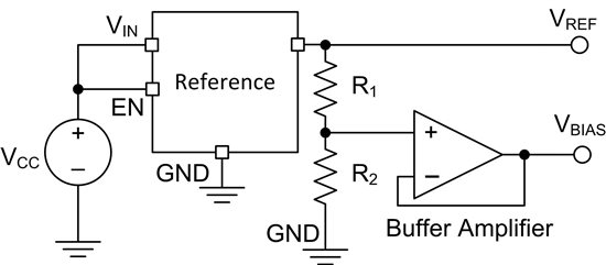
Figure 1 depicts a discrete solution that provides a reference voltage (VREF) and bias voltage (VBIAS) based on the ratio of R1 and R2.

Figure 1: Dual reference discrete topology

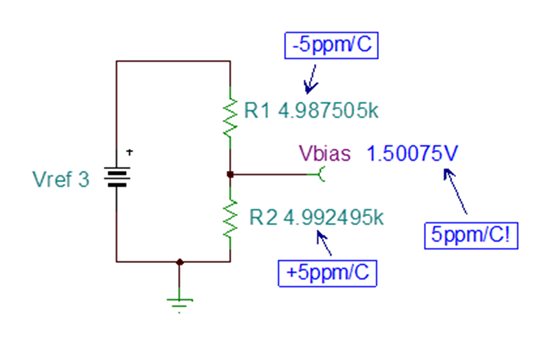
At the time it was ‘obvious’ that the overall drift of the resistor divider is (5 ppm/°C) + (5 ppm/°C) = 10 ppm/°C.  Just to be sure, though, I ran a simulation.  Figure 2 depicts the result of the TINA-TI simulation where R2 drifts in the positive direction, R1 drifts negatively, and the change in temperature is 100°C.

Figure 2: Vbias after R1 and R2 drift

Calculating the gain error yields 0.05% (500 ppm or 5.0 ppm/°C), which is the drift of one resistor…not their sum! 

Now let’s examine the familiar voltage divider circuit’s gain ratio and re-arrange it as shown in Equation ( 1 ).

 Where


α is the ratio of R1 and R2, and ultimately relates to the gain of the circuit.  For example, if α=1, the gain is ½.  So, as α→0, the gain→1.  Similarly, as α→∞, gain→ 0.

The actual gain of the circuit over temperature will depend on the drift of the resistors, which is shown in Equation ( 3 ) by δ.  To be consistent with the simulation, R2 drifts positively and R1 negatively.


Equation ( 4 ) calculates the gain error.  For simplicity, it is not converted to a percentage (if you want to do that, simply multiply it by 100 but be careful when converting to ppm).

 Using Equations ( 1 ) to ( 3 ), Equation ( 4 ) simplifies to:


Notice that the gain error depends on both the drift (δ) and the circuit gain (related to α).  Furthermore, if α=1 (circuit gain=½), the gain error simplifies to δ, which is exactly what the simulation shows!

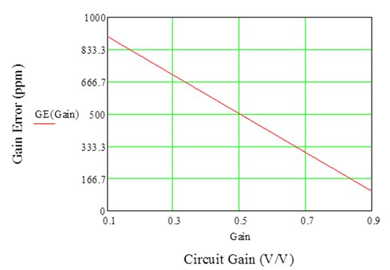
Figure 3 is a plot of the gain error versus the circuit gain for this design (5 ppm/°C resistor drift, or 500 ppm total drift over 100°C).  Notice that the gain error is 500 ppm when the circuit gain is ½.  Also notice that as the circuit gain increases, the gain error decreases and vice versa.


In summary, the drift of the voltage divider was not as expected…it is not the simple sum and it depends on the circuit gain.  So, next time you’re designing a circuit and come across one of those ‘obvious’ conclusions, you may want to double-check it with TINA-TI!

If you have any similar ‘obvious’ experiences, please share them in the comments section!

Register for MCU Design Days 2014

$
0
0

Join us for MCU Design Days 2014 on July 14th and 15th in Dallas, TX.

MCU Design Days will consist of two days of technical lectures, labs and demos. You will walk away with tools, increased knowledge of TI's MCUs and Wireless Connectivity products and software, as well as the right contacts to help you get your projects off the ground. On July 14th, we will start with keynotes from the Texas Instruments MCU Management team and end the day with an evening demo event with demos, collateral and representatives from TI and third party partners. On July 15th, we will have a full day of training sessions, including hands-on labs.


Here is a breakdown of what's included:

  • Customized schedule for each customer – Customer has the choice to choose between 24 technical overviews and hands-on training

  • Networking with TI MCU management and engineers– Get answers and get your projects kicked off

  • Walk away with free tools and LaunchPads – Select two LaunchPads of interest and we’ll have them ready for you at check-in!

  • Evening demo and happy hour event is included in registration – See demos from TI and our third parties. Also, interact with marketers, applications engineers and management from TI’s Embedded Processing businesses

  • Breakfast and lunch included daily  

  • See the agenda& abstract here

All of this is available for a registration fee of just $99!

 Sign up today to reserve your spot!


PowerLab Notes: My personal IoT and how I would power my favorite

$
0
0

The IoT is everywhere!  As my buddy Brian said in his last post, the Internet of Things is here and continuously growing.  As an exercise in my own curiosity, I decided to scour the house and figure out exactly how many things we have connected to the internet.  I was a bit surprised. I am junky for electronics and the latest gadgets, but this is out of control!

34 Products in or around my house are connected to the internet.  Here is the breakdown


  • 6 IP Security Cameras
  • 2Wireless Routers
  • Internet Modem/Gateway
  • Wireless Printer
  • 3 Gaming Systems (PS2, PS3 and Wii)
  • Smart Thermostat
  • AV Receiver
  • 3 IP Cable Set Top Boxes (STB)
  • Smart TV
  • Digital Photo Frame
  • Smart Programmable Remote
  • Home Theater PC (HTPC)
  • Water Meter
  • Power Meter
  • Natural Gas Meter
  • 3 iPads
  • iPod Touch
  • 2 iPhones
  • 2 Dell Notebooks
  • MacBook Pro


How to power all of these devices?  Most of the items listed above come with some sort of external adapter that takes the AC line and converters to an intermediate voltage.  These devices are generally the lower power (up to ~65W) consumers. 

There are a few that are not powered from external adapters.  The smart TV, AV Receiver, STBs, HTPC, PS2 and PS3 all have built in AC/DC power supplies. These devices require more power or multiple outputs, so the AC/DC built into the product makes sense. 

The only devices left are the Nest thermostat and the utility meters. These devices have a unique way of getting power.  The utility meters use the AC line, battery power or flow to power the meter communications. The last device (Smart thermostat) not only has a unique way of getting its power, but it is my favorite.

Thermostats have a unique power system that has been used for many years. The air handler unit is connected to the AC line. This unit has a small transformer used to step the voltage down from the house mains to 24VAC.  The 24VAC is used to power a number of relays that control the on and off functionality of the different modes in the HVAC system.  These relays are controlled by the thermostat.  The 24VAC is fed to the thermostat; this voltage is used as the main source of power. 

In the case of the Smart thermostat, there is also a battery to supplement the AC power.  The battery is necessary to provide peak power for the LCD screen, Wi-Fi transmissions and various other functions.

Here is how I would power a Smart thermostat.  Since I paid $249 for the thermostat, I am not real excited to take it apart and find out what is inside. There are a number of teardowns on the web, but most of those have little or no concern with the power system.  I also don’t have all of the power specifications, but this is what I do know:

  • 24-V AC Input
  • 3.7-V LiPO Battery
  • AM3703CUS Sitara ARM Cortex A8 microprocessor
  • TPS65921 PMIC and USB

I am going to assume that the battery powers the TPS65921, which in turn powers the Sitara processor

So, how do we get from 24-V AC to a voltage that can be used to charge the battery?  The easiest and most practical way is to rectify the AC voltage, store it in a bulk hold up capacitor, then buck down to 5V.  Rectified 24-V AC produces a DC voltage of around 33.8V, if we add 20% to that value, the max DC voltage is 40V.  Again, I am assuming that 5V @ 500mA will be enough power to charge the battery.

Many, Many IC Choices! TPS54140 is just one IC that would work great for this application. This is 42V max input voltage and provides up to 1A output current. PMP4746 is an example of a circuit that could be used in this situation. This circuit has the added advantage of providing some extra input filtering to reduce reflected noise on the input line. The 5-V can then be used with a BQ single-cell charger.  There are a number of chargers that can be used.  Two examples are a linear charger (BQ2408x) and a switch mode charger (BQ2415x).  Not too complicated of a system once it is all broken down.

This was an eye opening exercise for me.  I have no idea if my use case is typical, but I certainly didn’t realize I had that many devices.  How many do you have?


CONTEST: #ISpywithTI the smallest LDOs

$
0
0

We’re celebrating our small size LDOs, and you could be a winner! Our LDOs are so small sometimes it’s hard to find them among even the tiniest things. This week we have hidden our small-size LDOs in photos of tiny, everyday items. If you can find the LDO, you could win an EVM package that includes the TPS7A3501EVM-547, TLV71333PEVM-171, and TPS54120EVM-103.

How to enter:

  1. Follow us on Twitter. Follow @TXInstruments to see the three photos that have the hidden LDOs.
  2. Find the LDO. When you find the LDO hidden among the other tiny items in the photo, retweet the photo with the hashtag #ISpywithTI and you’ll be entered to win.
  3. That’s it! We will select three winners, one from each photo. Only one retweet of each photo will count as an entry.

*Open to legal residents of the United States and the District Of Columbia who are at least eighteen years of age.*

Read the OFFICIAL RULES.

Don’t forget to stay tuned to our @TXInstruments Twitter page and be on the lookout for the small-size LDOs hiding among everyday items. You can also receive updates about the contest  and all of our power solutions by subscribing to the Power House blog (top right corner).

Good luck!

Revolutionary new tool allows devices to use smaller batteries and last longer between charges

$
0
0

One of the top concerns for nearly every electronic device we use today is how much power can we get out of it. We want our smartphones, computers, power tools and wearable fitness devices to use less power so they last longer. That’s why TI announced a new technology for engineers, who use TI MSP430™ microcontrollers (MCUs) in their electronics, to be able to know exactly where and how devices use power.

 This new technology is called EnergyTrace++™, which is a power profiling system. Basically, engineers spend a lot of their time looking for ‘bugs’ in the MCUs that run their devices. These bugs, or tiny errors in the software that run a system, can result in an increase in unnecessary power usage. In order to find these bugs in inexpensive MCUs, engineers would previously have to use a meter to go over every line of code in an MCU – a very time-consuming process. Now, with EnergyTrace++ technology, all of the power information is displayed in a graph on an engineer’s computer screen, showing exactly where and how much power is being used depending upon what action a device is performing.

“Energy Trace++ finds bugs that are eating up extra power by enabling the MCU to show you how much power is being consumed doing any action, instead of passively measuring power consumption outside of the MCU with a measuring tool like a multimeter,”said Priya Thanigai, MSP430 Product Marketing Engineer.

Priya said this type of tool has existed in the past, but with a big catch. Previously, if an engineer wanted to find these tiny bugs deep within the software of an MCU, they had to spend thousands of dollars on very expensive MCUs and equipment, plus the engineers would have to have a lot of knowledge as to how the debugging tool works. EnergyTrace++ is inexpensive and easy to use for engineers in small start-up companies in garages all the way up to multi-million dollar corporations.

“The fact that you can do this on an inexpensive MCU like the MSP430FR59x/69x FRAM MCU families is what makes this product so unique and innovative, in that the circuitry lets you get that level of accuracy and detail without having to spend the money on it,” she said. “With EnergyTrace++, you can get setup in less than five minutes, you spend less than $25 and the kind of performance you get out of it would typically only be found in a really high-end tool.”

William Cooper, a MCU product marketing engineer, believes this debugging tool will enable battery-powered devices to use smaller batteries, last longer periods of time between charges or in some cases remove the batteries altogether. He also believes that since this technology is so easy to use and quickly finds bugs, companies will be able to get their products to market faster.

“This is one of the most innovative tools for development we’ve had in a decade, and it’s getting a lot of people excited, and frankly, we’re excited to talk about it and get it out there for people to use,” said William.

Click on the following links to find out more about the MSP430FR59x/69x FRAM MCU families, the MSP-FET MSP430 JTAG programmer/debugger  and the MSP430FR5969 LaunchPad rapid prototyping kit that make EnergyTrace++™ technology possible.

Infotainment Innovation

$
0
0

Advances in in-car infotainment systems have always struggled to keep pace with the fast innovation in the consumer space, and the mobile era has exacerbated the gap in recent years. There have been several innovative solutions in the infotainment market to bridge this gap.

Even though the features of the infotainment systems have increased recently (touch control, Pandora radio, and speech recognition) these features have generally been incremental and lagging behind smart phones and tablets due to the difficulty to achieve automotive robustness and/or address safety concerns.   The automotive market would benefit from a similar such transformation inside of the car and in many ways is already moving that direction.  This “makeover” cannot simply include a bridge of features from a phone to the car:   there are many key differences between mobile devices and the in-vehicle environment including:

User Interface and Driver Distraction

  • User interaction with an infotainment system is significantly different from that of a mobile device. In the mobile context, the user’s main focus is on the device and the screen.  In a driving environment, the driver is focused on the road, controlling the infotainment system without distraction. It is frightening to see a driver sending text messages and checking his/her Facebook page on his/her mobile device while driving. These distractions put many lives in danger. As the infotainment system integrates more features, driver interaction without system distraction increases in criticality. This is an area with a significant amount of room to innovate on the user interface and to prevent driver distraction:  improved speech recognition; text-to-speech; multi-touch, haptic and gesture displays are just some methods that are being deployed and explored to improve the intuitiveness and safety of the interaction between driver and vehicle. This is an area with a significant amount of room to innovate on the user interface and to prevent driver distraction.  Haptic feedback on touch interfaces is a particular area where TI is working and has been shown to improve the overall safety of vehicle infotainment interfaces and reduce driver distraction.  Other innovative user interface technologies include:  improved speech recognition; text-to-speech; multi-touch and gesture recognition.

Mobile Connectivity

  • Seamless integration with mobile devices is an important topic to enable drivers to extend their digital lives into the vehicle. In general, the interactivity between mobile devices and infotainment systems needs to become much more intuitive and seamless. Sharing content between the carry-in device and the vehicle needs to be transparent without requiring intervention from the end user. This still requires innovation in how the car presents mobile apps and content

Driver and Passengers

  • Phones are used by a single user at a time. However, in the vehicle context, passengers may also desire to interact with the infotainment systems. Their needs from the system are different simply due to the fact that they are not driving.  Infotainment systems which allow for a customized experience for the driver and passengers alike can provide a further enhanced and tailored experience, which should improve the appeal of such systems as well as customer satisfaction.

Auto-specific features

  • Cars are like black boxes for most owners: if anything goes wrong, they take the car to a mechanic to solve the problem. With the options for external connectivity available in many cars now, car-centric information can be made available remotely, which enable the app developers to create to auto-centric applications, to help drivers with safety, maintenance, and usability of cars. For example, the Link accessory from Automatic Labs enables the car to be connected to a smartphone over Bluetooth® and provide information on driving speeds, braking, MPG, etc. through a smartphone app.
  • There are many safety related features that can be integrated into infotainment systems to further assist the driver. These features may include surround view/overhead view capabilities, lane departure warning, traffic sign recognition, pedestrian detection, etc. Currently, these features are available in some cars but are generally distinct and disconnected from the infotainment systems. Improved interaction of certain of these features into the infotainment system should provide a more cohesive and intuitive interface for driver and potentially reduce the system cost, making these features more accessible in the market.

Firmware Upgrade

  • In modern automotive systems, there is no easy way of updating firmware installed at the factory.  The fast pace of innovation in infotainment systems requires a reliable, easy-to use mechanism for updating the ever-increasing software/feature capabilities of the system. Considering that cars are not replaced as frequently as mobile devices and used by drivers for many years, upgrading infotainment firmware becomes a critical component to keep up with technology advances.

Some of these features have featured prominently in a few cars, but widespread propagation of many of these items is underwhelming. Considering that infotainment systems are now one of the car’s key selling features, a transformative infotainment system will have a huge competitive advantage.  

Texas Instrument’s “Jacinto” family of infotainment processors enables automotive Tier-1s and OEMs to bring exciting and highly-capable infotainment systems to the market. With the “Jacinto 6” family, TI enables a rich software ecosystem to take advantage of performance and scalability to ride the wave of innovation just around the corner. Read more about the newest member of the “Jacinto” family, “Jacinto 6 Eco”, on a recent Behind the Wheel blog post.

Here we grow again! MSP430 expands its portfolio of FRAM-based MCUs with the MSP430FR5x/6x series

$
0
0

Are you trying to add functionality to a system with a reduced or equivalent power budget? Do you spend countless hours trying to locate sources of leaking power in your system? Are your production costs expanding as you increase functionality to your system? Would you like to form your system around a microcontroller with a clear migration path to higher memory footprints?

The  ultra-low-power MSP430 FRAM-based microcontroller family is now expanding and can help solve your problems from development to production. The MSP430FR59xx and MSP430FR69xx  MCUs with nonvolatile FRAM memory ranging from 32-128 KB, are now available and ideal for a broad set of applications that require ultra-low-power consumption, flexible memory options and smart analog integration. FRAM's 250x lower power and 100x faster write speeds are just the tip of the iceberg!


Similar to other MSP430 microcontrollers, the new FRAM devices offer key advantages in terms of ultra-low power, integrated analog and digital peripherals, and ease of use. 

Ultra-Low Power

  • Built on a new ultra-low-leakage 130 nm process and leverage the strength of MSP430,  our FRAM MCUs are lower power than ever before!
  • Enabled by FRAM, flexible clocking, and more!
  • By the numbers:
    • Active Mode: 100 uA/MHz.
    • Standby with RTC: 450 nA.

Smart Analog and Digital Integration

  • Differential ADC with integrated window comparator can operate without CPU intervention.
  • Hardware peripherals for multiplication and AES encryption (256-bit).
  • Built-in LCD and Scan IF save space and power in a number of applications.

Ease of Use


So, are you interested in the world’s lowest-power microcontrollers? Head over to www.ti.com/fram to learn more and stay tuned for more information on the support ecosystem surrounding this family.

Viewing all 4543 articles
Browse latest View live


<script src="https://jsc.adskeeper.com/r/s/rssing.com.1596347.js" async> </script>