Quantcast
Channel: TI E2E support forums
Viewing all 4543 articles
Browse latest View live

How low can you go? New benchmark measures application-level power efficiency

$
0
0

In the past several months, we released nearly 100 new Ultra-low-power MSP430FRxx FRAM microcontrollers. Our collateral calls these microcontrollers out as the lowest power in the industry, but you don't need to take our word for it! It is important to evaluate microcontroller power efficiency based on a number of factors. These can include:

  • Active mode current consumption
  • Low power mode current consumption
  • Peripheral current consumption
  • Memory current consumption required to read/write

To make choosing the right microcontroller easier, The Embedded Microprocessor Benchmark Consortium (EEMBC) offers a number of benchmarks. For reference, this is the same group that created the COREMARK® benchmark. COREMARK is a benchmark that isolates a CPU's core performance by focussing on the CPU pipeline. This benchmark offers a simple starting point for comprehension of MCU performance, but does not provide a true measure of performance in applications where low-power matters. To address these types of applications, the EEMBC has released a new benchmark called ULPBench™!

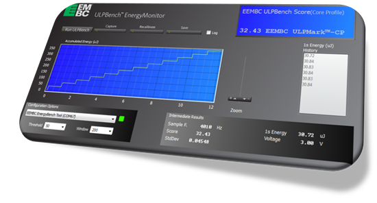
The ULPBench offers a two prong approach including the benchmark itself on the software side and an EnergyMonitor hardware tool. These components account for the ability of a microcontroller to operate efficiently in applications where time spent in active mode is minimal and waking up on a precise interval can be critical. Typically, integrated hardware can also play a huge role in low-power applications as well. This hardware, such as 32-bit multipliers, AES encryption engines, and direct memory access reduces software complexity and can significantly reduce cycle times in active mode. By considering these factors, ULPBench offers an apples-to-apples comparison between microcontrollers in a way that focusses on real-world applications. 

Scores are already available showcasing the power efficiency of the new Ultra-low-power MSP430FR5969 FRAM microcontroller compared to other competing MCUs. This new benchmark can also be used across microcontrollers with the EEMBC ULPBench EnergyMonitor, which is an accurate tool for measuring energy that comes with a convenient GUI for data capture! This tool is available today so that developers can get the numbers for themselves!

After using the EEMBC EnergyMonitor to evalaute different microcontrollers across the industry, you may be ready to get started with the MSP430 MCU ecosystem. Don't forget that we also have an energy measurement tool for making sure your system is as efficient as possible during your design cycle! EnergyTrace™ technology enables real-time measurements from nano-amps to milli-amps and on devices like the new MSP430FR5969 or the MSP430FR6989 FRAM microcontrollers, provides CPU and peripheral state information!  

 Ready to get started? Grab the MSP-FET or one of our new FRAM MCU LaunchPad development kits to start your evaluation today! 


What’s all the noise about sensorless BLDC motor drivers?

$
0
0

Creating a drive system for three-phase brushless DC (BLDC) motors has always been a task of balancing a handful of system requirements. Care-abouts such as efficiency, reliability, development time, protection, acoustic noise and cost have always been and are key driving factors for decisions on part selection. A sensorless, BLDC motor controller could help put your worries at ease.

In a previous post, Milan Rajne discussed how the DRV10983 cuts development time and cost. Today, I want to focus our conversation on the acoustic performance of BLDC motors and how the DRV10983 motor driver quiets the competition. Whether it is a fan humming while you are trying to sleep or a small pump buzzing in an otherwise quiet atmosphere, acoustic noise from motors can be a real annoyance.

To really grasp the potential performance of a motor driver, let’s begin with where the noise comes from. In traditional trapezoidal control, or 120° control, when the motor phases are commutated it leads to abrupt changes in the phase currents.  These changes cause torque ripple in the motor, which in turn cause audible vibrations. Because the drive state changes every 60°, there are noticeable pure-tones introduced at harmonics of 6x the motors electrical frequency. To significantly reduce these pure-tones we can use a different method to drive the motor.

Sinusoidal control, or 180° control, benefits from driving all three phases to better control the torque. As the name suggests, this method controls the motor by driving the phases with sinusoidal voltages to avoid any abrupt changes in current. This smoother drive method reduces torque ripple which, you may have already established, reduces audible noise. Figure 1 shows an audio analysis of the DRV10983 using sinusoidal drive versus a leading competitor using trapezoidal control. The electrical frequency is 40Hz, and you can see the significant pure-tones at 240Hz, 480Hz, 720Hz and 960Hz. Notice how the DRV10983 is able to reduce each of these audible frequencies?

Figure 1: Audio data comparing DRV10983 to a competitor

The DRV10983 utilizes sinusoidal control to reduce noise during normal operation; however, this is not the only technique in this highly configurable device to keep things quiet. During standard startup of a sensorless BLDC drive, there is typically a short period of alignment. This alignment ensures the motor will be in a known position for reliable startup. The major downside of this is that to align the motor, the phases must be excited quickly. This fast excitation causes a useful torque to turn the motor but, along with that sudden torque, comes acoustic noise.

To avoid this we have made the excitation profile of the motor adjustable. Not only does this let you tune the startup time and strength, you have the power to reduce the audible noise of your system. Taking this a step further, some applications can make use of a different startup method: initial position detection (IPD). With the DRV10983, the engineer can select to use IPD; and, just like with the align method, they can control the excitation limit of the IPD routine.

Listen to these audio clips to see what all the buzz is about!

Competitor start-up noise
(Please visit the site to view this audio)

DRV10983 start-up

(Please visit the site to view this audio)

These features of the DRV10983 enable any engineer to balance their systems priorities. Click here for more information regarding the specifications of the DRV10983, including explanations for startup and drive methods. Let me know how you’ve dealt with these noise challenges before. Will the DRV10983 solve your problem?

For more information:

TI and the United Way take STEM outside of the classroom

$
0
0

Teachers constantly find themselves challenged to bring to life the concepts found in a textbook. TIers, with the help of a Dallas Cowboys Hall of Famer and volunteers from the United Way of Metropolitan Dallas, recently helped teachers with that challenge in science, technology, engineering and math (STEM).

Our president, chairman and CEO Rich Templeton helps a Hamilton Park

Pacesetter Magnet Elementary School fifth-grader power a calculator with a potato.

Football legend Tony Dorsett and TIers from Dallas spent much of Oct. 20 engaging in hands-on STEM activities and experiments with about 100 fifth-graders from Hamilton Park Pacesetter Magnet Elementary School.

The students went from station-to-station on the school’s playground, learning how to power a calculator with a potato, construct solar ovens with little more than a pizza box and tinfoil and create pulley-and-lever systems with LEGOs. Every step of the way, a TIer was there guiding them through the activities.

“Events like this are about making sure students like you really learn about STEM, because it is the foundation of your future,” our president, chairman and CEO Rich Templeton told the fifth graders.

Students had the opportunity to take part in activities supported by the Perot Museum of Nature and Science, REAL School Gardens and the Frontiers of Flight Museum.

As part of the day’s events, Tony, the Super Bowl champion and Heisman Award winner, spoke to the students about the importance of putting schoolwork first.

“Sports will come and go, but your education will last a lifetime,” he told the students. “I know you have big dreams, and keep dreaming big. But the road to fulfilling your dreams is through education.”

(Please visit the site to view this video)

The event at the Richardson Independent School District school was the latest in the TI-sponsored “Nine for 90” program, the United Way of Metropolitan Dallas’ year-long 90th anniversary celebration.

“Year in and year out, TIers come back and share their hearts with our community,” said Jennifer Sampson, president and CEO of United Way of Dallas.

A TI volunteer shows a Hamilton Park Pacesetter Magnet Elementary

School fifth-grader how to construct a pizza box solar oven.

The nine community service projects focus on United Way’s three pillars for strong communities:  education, income and health. This month project featured a “STEM in the Schoolyard” approach to create memorable moments for students with math and science. TI has been a strong supporter of United Way in Dallas for more than 50 years, with education at the heart of the company’s philanthropy and volunteerism, particularly aimed at improving STEM education for females and minorities who are underrepresented in the science and engineering fields.

We believe that diversity fuels innovation, and that’s why we focus our efforts on schools like Hamilton Park Pacesetter Magnet, where students develop in a multi-cultural environment through innovative and diverse learning experiences.

According to the American Society for Engineering Education, of those graduating with electrical engineering degrees from U.S. universities, less than 15 percent are women, less than 10 percent are Hispanic and about five percent are African-American.

“Women and minorities do not always get the same access to hands-on learning and opportunities to speak with real-life engineers like some of the TIers at this event at Hamilton Park,” said our chief citizenship officer Trisha Cunningham. “We are committed to programs and activities like this in our own backyard that can get students excited about STEM.”

That’s why we are so heavily involved with efforts in Dallas, and across the U.S., where the focus is on the next generation joining the STEM workforce.

“We believe all students should be regularly exposed to interesting and important STEM learning so they are much more likely to pursue a STEM degree,” Trisha said. “And we believe a math- and science-capable workforce is essential to a future filled with innovation.”

Programs like this “STEM in the Schoolyard,” and the more than $150 million we have invested in the last five years in education efforts, helps fuel students’ passion for creativity and interest in problem solving with the goal of hopefully one day working in a STEM field.

For more information on our ongoing efforts in STEM and diversity, visit @AroundTI and ti.com/education.

Choosing the right sense resistor layout

$
0
0

There are many things that can go wrong when designing with a hot swap controller. For example, the hot swap can trip at an unexpected current value or a current monitor may report inaccurate measurements. As a result, the integrity of a system which relies on protection by the hot swap can now be at risk. Optimizing sense resistor layout by using four pads can help avoid failures and create a robust hot swap design.

It is important to understand that sense resistors can be very sensitive. Factors such as size, type and manufacturer can lead to varied results. The idea of using four pads with a two terminal resistor to optimize measurement accuracy can hold true for some resistors but not for others. Ensure your design is operating as expected by testing it with your sense resistor and layout in the prototyping phase of your development. If you are looking for a tested design to quick start your development, simply copy the BOM and layout from one of TI's Hot Swap Controller EVMs such as the TPS2490, LM5067 and the LM25066I!

The sense resistor, RSENSE, is a key component for sensing current with a hot swap controller. As power requirements in server and telecom applications increases, sense resistors as low as 300µΩ are becoming more common. At these levels,effects such as solder resistance can play a significant role in throwing off your measurement. Let's take a look at a simple two pad current sense:

Since we are measuring the voltage at Sense + and Sense -, we must look to the golden rule V = IR. Since current is constant throughout RSOLDER+ RSENSE + RSOLDER, the current sensed, ISENSE = (VSENSE + - VSENSE -) / (RSENSE + 2RSOLDER). For example, if RSENSE = 300mW and RSOLDER =  15mW, then your current measurement will be off by a factor of 10%. Avoid these inaccuracies by adopting four pad sensing.

There are several layouts you may choose from for your sense resistor. We will discuss three of the common choices, but first let’s understand how four pad sensing works.

The layout is broken out into four pads. Two of these pads (RSOLDER) carry the high current flow while the two remaining pads (RSOLDER_S) carry very little current, virtually 0A.  This eliminates RSOLDER in the equation and the result is  ISENSE = (VSENSE + - VSENSE -) / RSENSE. Now the accuracy of the current measurement is purely dictated by the accuracy of RSENSE and the measurement of VSENSE .

A four pad solution is not always the answer; the three figures below outline the pros and cons of three common layouts:


Figure 1 is a simple two pad approach, but note that the sense lines are taken from the inner center of the chip. The high currents flowing on the sides of the connection are balanced, allowing a good measurement of VSENSE + and VSENSE - . This type of layout is simple to route and is easy to assemble on a PCB. This layout is recommended for designs where the value of RSENSE is relatively large compared to RSOLDER (100:1).

Figure 2 is typically the best layout for accuracy as the sense lines route to the inner center of the chip and uses four pad sensing. The drawback to this approach is that the pads have a higher risk of getting shorted in assembly. If this occurs, you may not see the short since the resistor can be covering the pads; this would result in a two pad sense.

Figure 3 is another four pad sense layout, but the sense pads are at the bottom. This layout is easier to assemble than Figure 2 and you can easily see if there are any shorts between the pads.

Each of the three layouts have been used and tested on TI hot swap EVMs. Figure 1 and Figure 2 layouts are recommended for sense resistors in package type 2512 or smaller. Figure 3 layout is recommended for larger or specialty sense resistors which may incorporate cutouts such as the 3921 size resistor used on the LM25066I EVM.

Thanks! -Alex

SAR ADC response times

$
0
0

This is the second post in our SAR ADC series.

Part 2: A marketing analogy

When a response time of 1 µs is required from the SAR ADC (tRESP-ADC = 1 µs), many engineers would search for a SAR ADC with throughput of 1 Msps (tTHROUGHPUT = 1 us). In reality, the two parameters are actually different. To demonstrate the difference, let’s look at the following analogy:

You are the marketing manager of a major retail company. The company plans to launch a new e-tailing business in order to maximize its customer base. To start,you  identify 3 essential steps in the e-tailing process:

  1. Understand customers’ requirements
  2. Identify the correct product
  3. Execute payment through a secured, external, payment gateway

You supervise two teams, Team A and Team B, to design the e-tailing portal. To maintain high quality of service and to maximize profits, you set up following goals for both teams:

  1. Maximize number of customers addressed per day
  2. Achieve score of >80 on customer satisfaction rating

Once both teams are ready, you release a ‘Beta’ version from each and launch a survey.  The survey results are shown below: 

The results show that:

  1. For users with a high bandwidth connection, Portal A can address ~10% more customers per day. Even for customers with  a low bandwidth connection, Portal A is still able to address same number of customers per day – a whopping ~20% more than what Portal B could achieve.
  2. For all ‘Other Parameters’, both the portals have similar ratings.

 Portal A is the clear winner on ‘throughput’– i.e. on maximizing number of customers addressed per day.

However, rather surprisingly, the better portal (Portal A) also has a poorer customer satisfaction rating! As any clever manager would, you dig deeper into the time taken by each portal for several key steps in the process:

Moreover, what you discover is that these two charts provide a completely new story:

  1. By improving the questionnaire given to customers, Portal B took less time to ‘Understand Customers’ Requirements..
  2. By improving the search algorithms, Portal B was took less time  to ‘Identify the Correct Product.’
  3. Both Portals took equal time on the External Payment Gateway to ‘Execute Payment.

In summary, the customer satisfaction ratings are inversely proportional to the ‘response time’ of the portal – i.e. the more the time customers have to spend on the portal, the lower the ratings.

No wonder customers gave higher rating to Portal B!

That brings us to the real question:

If Portal A was taking more time to address each customer, how was it able to address more customers per day than Portal B? In other words, if Portal B had a better ‘response time’ than Portal A, how could Portal A achieve higher ‘throughput’ than Portal B??

On closer inspection, you figure out that both portals are executing the first two steps ‘in-house’ and then connecting the user to an ‘External Payment Gateway.’ In summary, you have discovered that the trick is in the effective utilization of time spent at the ‘External Payment Gateway.’

Therefore, after completing the first two steps and connecting the customer to the ‘External Payment Gateway,’ Portal B sat idle – waiting for the payment transaction to complete.

Portal A, however, had figured out that it need not stay idle during this time!

Portal A was able to ‘Understand (next) Customers’ Requirements’ even as the external payment gateway was ‘Executing Payment” (for previous customers).

By implementing this ‘parallel processing’ technique, Portal A completely eliminated the ‘Execute Payment’ step from their ‘throughput’ calculations. This method also allowed Portal A to address the same number of customers irrespective of the connection bandwidth.

However, this increase in throughput did not improve the response time of the portal, thus explaining the poorer customer satisfaction ratings.

Coming back to SAR ADCs, a typical SAR ADC goes through three states:

  1. ‘Sample’ the Analog Input
  2. Convert the ‘sampled Analog Input’ to ‘equivalent Digital Code’
  3. ‘Transfer’ the digital output code to the host controller

Do you see the similarities now?

Stay tuned – in the next blog post we will learn how SAR ADCs can achieve higher throughputs without actually improving the response time. 

JESD204B: Understanding subclasses (part 2)

$
0
0

In my last post, I explained the importance of JESD204B subclasses and reviewed the details of subclass 0 and 1. Today, I’ll explore subclass 2.

Subclass 2

Subclass 2 analog-to-digital converters (ADCs) and digital-to-analog converters (DACs) have a local multi-frame clock (LMFC) similar to subclass 1. The devices use LMFC to establish a timing reference and alignment point. In subclass 2, the logic device LMFC will always act as the master LMFC reference point, and any attached ADCs and DACs will re-align their LMFC to match the LMFC within the logic device.

In general, the SYNC signal is aligned to the LMFC and communicates a request to start code group synchronization (CGS). It also indicates the LMFC position. The SYNC signal in this case is critical, and you must route this signal with some care to ensure it meets the sample and hold times of the device clock. For multiple data converters connected to a logic device, all of the device clocks and SYNCs must be skew matched to achieve device synchronization. 

If you need to connect an ADC to the logic device, the RX logic device will drive SYNC low to start CGS. This SYNC signal going high will establish the LMFC edge within the ADC. For multiple ADCs connected to a logic device, the SYNC signal to each ADC must be trace-length matched to ensure you establish the same LMFC in each ADC, resulting in the same deterministic latency.  This ensures that the multiple devices are synchronized. Figure 1 shows the timing connections for an ADC connection to the logic device.

Figure 1 – ADC connections for subclass 2

When you need to connect a DAC to the logic device, the DAC will be the RX device.  The DAC RX device will drive SYNC low to the TX logic device to start CGS. It also tells the logic device where the DAC LMFC is relative to the logic device LMFC. 

Since the logic device acts as the master LMFC reference, it will send back configuration messages in the second frame of the initial lane alignment sequence (ILAS) multi-frame to indicate if the DAC LMFC requires adjustment. The TX logic device will send back the following parameters to the DAC:

PHADJ - is a 1-bit signal that indicates if you need to adjust the DAC’s LMFC

ADJCNT - is the number of resolution steps needed to adjust the DAC’s LMFC (TX logic device must know the adjustment resolution of the DAC)

ADJDIR - is the direction of the phase adjustment – 0 advance, 1 delay

The DAC will receive these messages in the ILAS configuration multi-frame and adjust its LMFC accordingly before toggling SYNC again. This will send another CGS request to the TX logic device to see if the adjusted LMFC is aligned. This process will continue until ADJCNT=0. This should ensure alignment between the LMFCs of the DAC and TX logic device. 

With the LMFC aligned, you can achieve deterministic latency between the DAC and the TX logic device.  If you achieve the same deterministic latency on multiple DACs, you will achieve multiple device synchronization. Figure 2 shows the timing connections required for subclass 2 with multiple DACs.

Figure 2 – DAC connections for subclass 2

The standard recommends that designers not use subclass 2 above 500 Msps, but instead use subclass 1. As opposed to the SYSREF signal used in subclass 1, which is source synchronous with the device clock from the same clock chip, the SYNC signal is system synchronous. As a result, it is more difficult to meet setup and hold times at higher sampling rates. 

Summary

You must understand the three JESD204B subclasses and their implementation differences before deciding which subclass to use. For applications that require backwards compatibility to JESD204A, which has no provisions for deterministic latency, subclass 0 is the best choice. For applications that require deterministic latency or multi-device synchronization, either subclass 1 or subclass 2 can be used, with the caveat that subclass 2 should not be used above 500 Msps.

Stay tuned for next month’s blog, where I’ll discuss the process of verifying deterministic latency between an ADC and the logic device.

Additional resources:

Using software to solve the challenges of measuring system frequency response

$
0
0

Designing a power supply can be termed more of an art than a science. The transients and real-world interactions are simply too ornate to capture with any single model of a power supply system. Generally, these models construct some sort of transfer function that behaves as closely as possible with the plant or, in digital power designs, the power stage. In order to measure how close the real system behaves to the model and the control loop created to control that model, the power supply designer must measure the frequency response of the system. This data is then plotted on a Bode plot and analyzed to determine the gain and phase margin of the power supply controller design. In many cases, due to the inconsistencies between the model and the actual plant, this process is repeated multiple times during the power supply design process. This tuning of the control loop is where the artistic portion of power supply design comes into play.

Typically, frequency response measurement of power converters is done with help of an external frequency response analyzer.  This requires external connections and modifications to the board, including breaking the control loop path to perform analysis.

This method poses several problems for the power supply designer:

 1)      Inserting the resistor changes the characteristics of the system. No longer are you measuring the response of the pure control loop because you have broken the control loop path and inserted that small resistor.

2)      The process of taking these measurements is highly tedious and time-consuming.

3)      In most engineering labs, there are only a few network analyzers available and rarely are they just lying around. Vying for time to use this piece of equipment can be a full-time job in and of itself.

 So, what other options are there to measure the frequency response of a digitally controlled power supply system? Why, I’m glad you ask. One alternative is to use a software-based algorithm to inject the frequency into the control loop and measure the response of the system using the on-chip analog to digital converter (ADC), which is already connected in the control loop and measuring the output of the power stage. This process provides the plant frequency response characteristics and the open loop frequency response of the closed loop system. Software-based frequency response analysis removes all of the barriers mentioned above:

 1)      The control loop remains intact and unchanged

2)      The process is automated in software already embedded on the device in the form of a library

3)      No external measurement equipment is required.

 The process of implementing a software-based frequency response algorithm, as Texas Instruments has done with its latest software frequency response analyzer (SFRA) library is described in the following diagram.


Image used with permission from The MathWorks, Inc.


TI’s SFRA library is designed to enable frequency response analysis on digitally controlled power converters based on C2000™ microcontrollers using software only and without the need for an external frequency response analyzer. The optimized library can be used in high-frequency power conversion applications to identify the plant and the open loop characteristics of a closed loop power.

Software tool simplifies your digital power designs

$
0
0

Are you a fan of controlSUITE™ software as your one-stop shop for C2000™ real-time microcontroller (MCU) documentation and code examples? We have a new addition to the software suite to make it even easier for you to design your digital power applications.

PowerSUITE will include additional software infrastructure and tools designed to minimize development time for digital power supply designers. We just released the first tool in powerSUITE called the Software Frequency Response Analyzer (SFRA). The SFRA consists of a software library and GUI that simplifies the measurement of gain margin and phase margin of your power supply design.

The SFRA library can be integrated into your source code and requires no external measurement devices. Now you can quickly enable frequency response measurements on digitally controlled power converters based on C2000 MCUs without the need for an external frequency analyzer. All frequency response data will be displayed on the GUI and can be exported into an Excel spreadsheet for further analysis. For more information, check out our video.

Leave us a comment below and let us know how you will use the SFRA in your digital power designs.


DIYers make splash with water conservation project

$
0
0

TI software engineers Urmil Shah and Michael Erdahl have gotten smart about water conservation in the drought-beleaguered state of Texas.

Courtesy: Addison TreeHouse

As part of the NTx Apps Challenge, the duo spent 12 weeks developing a Web app and smart sprinkler system controller that incorporates weather data, neighborhood water usage and even municipal water restrictions to prevent the over watering of residential lawns.

The North Texas Commission, City of Dallas and University of North Texas sponsored the contest to tackle big issues in water, waste, energy and transportation in Texas.

“We had this idea for a sprinkler system because water is scarce, we’re in a serious drought and cities have watering restrictions in place,” said Urmil, who works in our test technology-product engineering group. “Yet, you drive around and see automatic sprinklers on while it’s raining outside. We had strong motivations for developing this project.”

So Urmil and Michael set out to build a smart system called “Sprink.ly,” which knows when to water (and when not to) based on local rain forecasts, soil conditions and other features. It uses a TI Sitara AM335x processor-based BeagleBone Black to control the sprinkler system from Amazon cloud services.

“Using advanced cloud-based weather forecasting data, our system knows when, and how much rain is coming, and alters the sprinkler schedule and run time based on the amount of precipitation that fell in your area.”

Urmil and Michael were rewarded for their efforts this month, when the NTx Apps Challenge presented them with a $10,000 check for their project in the Water Conservation category. The NTx Apps Challenge awarded $80,000 to five teams of Web entrepreneurs who created sustainability apps to address four key municipal growth challenges.

Sprink.ly consists of two components: the Web app and the hardware. Residents can use the free Web app to receive sprinkler reminders based on their city’s watering requirements and water recommendations based on hyper local weather conditions.

The “Sprink.ly” Web app is free to everyone; however, only city of Dallas residents will be able to track monthly water usage and other comparison data. Just type sprink.ly into your smartphone, tablet or desktop browser using Chrome or Firefox.

Watch a tutorial of the Web app here:

(Please visit the site to view this video)


An optional sprinkler controller uses the Internet of Things (IoT) and cloud computing to start the sprinklers, thereby providing a fully automated hands-free personalized solution. The hardware controller is still in prototype stage and not available to the public yet.

Urmil and Michael believe the system can save as much as 10 percent of the water used outside of homes. The average home in Dallas will use 10,000-15,000 gallons of water per month on a twice-weekly watering schedule, according to Urmil and Michael’s research.

“Our system will reduce water usage by only running the sprinkler system when necessary,” Michael said. “Traditional rain sensors only work after enough rain has accumulated in the device." 

Urmil and Michael said they were thankful for the opportunity to innovate and create something they had been thinking about for a while.

“We wanted to demonstrate this idea we had to conserve water and help our environment,” Urmil said. “Credit goes to Michael for making the prototype work.”

Ferroelectric materials could add value beyond FRAM and MSP430 microcontrollers

$
0
0

Ferroelectric material offers proven advantages in FRAM as an alternative to external flash memory or EEPROM. Over the past couple of years, the MSP430 MCU team integrated this technology into our ultra-low-power MSP430FRxx microcontroller family. This has led to the most recent line of FRAM microcontrollers with the industry's lowest power, the ability to retain more data on power failure and enhanced security features. Can the benefits of ferroelectric materials reach even further than microcontrollers?

Scientists in industry and universities are exploring the future of silicon transistors and believe ferroelectric material could bring unique benefits. This material could be used to switch between four different states, and could store these states without external power. As current technologies reach their limits, other materials like this may enable power and computational improvements. This could mean computers that can work faster while consuming less energy! Sound familiar?

Want to read on? Check out the full article by Katherine Bourzac in the MIT Technology Review.

Part 2 - Mitigating common mode noise

$
0
0

In my previous blog post, I outlined the fact that differential signaling can still be negatively impacted by common mode noise. In this post, I will outline some methods that you can use to reduce the impact of common mode noise on differential signal paths. I’ll cover three main categories of devices: passive circuits, high-impedance active circuits and low-impedance active circuits.

Let’s start with the simplest example, passive circuits. System designers often use an LC filter to eliminate noise. As commonly implemented, a differential filter will be floating with respect to ground. This is fine for the differential response, as shown in Figure 1. However, as shown in Figure 2, there is no attenuation of common mode signals. By implementing a simple change in the filter topology, as shown in Figure 3, we get the response shown in Figure 4.  

Figure 1: Filter differential response

Figure 2: Filter common mode response with 2.5k Ohm of common mode “termination”

Figure 3: Simple filter change to shunt common mode energy with one extra capacitor

Figure 4: Filter common mode response with change of Figure 3

Like filters, some active differential devices do not have any ground reference (or termination) for common mode signals. One example is the LMH6521 and other amplifiers with inductors connected to the output pins. The LMH6521 amplifier is a very high-speed, digitally controlled variable gain amplifier (DVGA). It has a fully differential signal path, with a 2.5k-Ohm common mode resistance, which is not sufficient for it to be a major attenuator of common mode energy, as shown in Figure 2. 

You can add more common mode energy dissipation to the LMH6521 by adding some resistors to the circuit, as shown in Figure 5. Through the beauty of differential signaling, the two 500-Ohm resistors add only 1000 Ohms of load to the differential circuit, but they provide 250 Ohms of common mode termination. The amplifier output load changes from 180 Ohms before the resistors are added to 152 Ohms after. This change in load condition will have very little impact on the amplifier’s performance, yet the common mode termination is much improved. The same technique could also be used at the amplifier input.  

Figure 5: Common mode termination of a differential amplifier (additional resistors shown in green)

Not all differential devices are high impedance with respect to the common mode. Some amplifiers, such as the LMH3401, have common mode control circuits that set the amplifier output common mode with a low-noise, low-impedance circuit. The LMH3401 has a common mode circuit that is basically a unity gain amplifier. It takes the voltage at CM and buffers it at the amplifier outputs, such that the common mode of the amplifier output pins is fixed. 

In Figure 6 below, I show the impact of this circuit as dotted capacitors. With respect to the common mode, the amplifier outputs are a virtual short to ground for any AC noise in the system. 

Figure 7 shows the common mode output impedance of the LMH3401. By selecting an amplifier with these features, you achieve built-in common mode rejection as an extra benefit, and you don’t have to do anything extra with your design.

Figure 6: Differential amplifier with low impedance common mode control

Figure 7: LMH3401 common mode output impedance (including on chip resistors)

As you can see, there are several ways you can help mitigate common mode noise pickup on differential signal paths. Some of them require a bit of planning and some extra components. An easier approach is to select an amplifier that’ll do the work for you.

Bonus:

Do you see the error in Figure 3? Leave a comment if you find it… 

Related resources:

Shhh, keep it down (out-of-band noise, that is)

$
0
0

 Nowadays, engineers designing audio systems for cars face many competing demands. Besides offering a superb audio experience, the design needs to abide by specific automotive system constraints, such as:

Weight and space: A vehicle that weighs less can hit mandated fuel economy targets more easily. Because every ounce in the car counts, audio designers place a premium on highly efficient systems (where no bulky heat sink is required) and solutions with few components. This is even more valuable in space-constrained head units and instrument clusters.   

Reliability: This is a key consideration for any equipment in the car, including the audio system.  It needs to withstand stringent automotive conditions and keep electromagnetic interference below industry-mandated limits, such as the CISPR25 L5 standard for electromagnetic compatibility (EMC).

This means designers have to juggle multiple tradeoffs across all the devices in the audio signal chain, like those in the very simplified block diagram below. 

Figure 1. Typical audio signal chain

In the DAC and audio amplifier portions of the audio signal chain, using a low out-of-band noise DAC can improve audio system design with the. Typical audio systems use a low-pass filter between the DAC and the audio amplifier to filter out-of-band noise.

What is a DAC’s out-of-band noise and why does it matter?

Any DAC will produce noise that extends well above audio frequencies, and this effect is strongest in delta-sigma DACs. These converters use noise-shaping techniques to improve in-band signal-to-noise ratio (SNR) performance at the expense of generating increased out-of-band noise.

Figure 2. Delta-sigma DAC noise shaping

It seems as if this would not be an issue in an audio system. Wouldn’t this out-of-band noise be inaudible as it is outside the audio band?  It can actually be a significant issue in automotive audio design.

As a sampled-data system, the Class D amplifier aliases the input signal. This means the DAC out-of-band noise is “folded back” in the audio band, increasing distortion and noise. And, as this out-of-band noise extends to higher frequencies, it can interfere with other devices. Most importantly, in the specific case of automotive audio, this can cause failure of mandatory and stringent automotive EMC tests, such as CISPR 25 L5. To provide the optimal converter performance, the out-of-band noise must be low-pass filtered.

What kind of LPF does my application need?

Sometimes, the most basic low pass filter (LPF), the RC filter, will do the job. But sometimes automotive audio designers find that an RC filter stage is not enough on its own. As the out-of-band noise depends on the DAC architecture, even active filtering may be required for the most common DACs. Active filtering adds substantial complexity, cost and additional components to the system.  And more components can increase the weight of the system as well. For example, some high-performance DAC applications require half a dozen passives, an operational amplifier and, potentially, a new power management stage to supply bipolar rails.


Figure 3. Suggested low-pass filter for a high performance DAC

To avoid this issue, DACs like the PCM5102A-Q1 use advanced current segment architecture to greatly reduce out-of-band noise, which could make the traditional 20kHz LPF a thing of the past in many automotive audio systems. Next-generation DACs like the PCM5102A-Q1 continue the legacy of TI/Burr-Brown innovation by using advanced current segment architecture to greatly reduce out-of-band noise, making a traditional 20kHz low pass filter a thing of the past.

Figure 4. PCM5102A-Q1

Improved mid-band out-of-band noise performance from the DAC translates to lower system cost and component count, since it requires no filter stage to minimize audio noise and distortion. In addition to the cost and component count reductions that eliminating the filter provides, PCM5102A-Q1’s low out-of-band noise at higher frequencies can make it easier to pass EMC tests, which can reduce development cost and time. This is particularly important when using electrically long traces and wires in systems capable of audio line-out.

By reducing out-of-band noise, audio design engineers can deliver a stellar in-vehicle audio performance, all while helping reduce costs and promote reliability for the system.


TI Innovation Challenge India Design Contest 2015 - The First Stop

$
0
0

Travelling via train during a festive season in India is a herculean task. The reservation counters, railway platforms and trains are heavily crowded with people confronting many challenges & travelling thousands of kilometers to reach home.The TI Innovation Challenge (TIIC) India Design Contest (IDC) train received a similar response on September 30th with over 3,100 student teams conquering a lot of technical and non-technical hurdles for submitting the proposal and boarding the TIIC train. We thank all the students and the faculty mentors for submitting a proposal in TIIC IDC 2015. 


The increased traffic

As always, the response to TIIC IDC has exceeded our expectation. We have also received an enthusiastic response from our first time participating select colleges in Sri Lanka.

Few interesting facts about TIIC IDC 2015

  • ~2x increase in college participation across all the regions (North, East, West & South).
  • 74 colleges have submitted >10 proposals to TIIC IDC 2015
  • >2,000 faculty members from 654 colleges have participated as faculty mentors in TIIC IDC 2015                                                                                                               

All the teams who have successfully uploaded their project proposal for the Qualifying Round of the contest are entitled to receive an e-certificate from Texas Instruments India University Program. These certificates will be issued by November 2014. 

 The results

Just as TTE(Train Ticket Examiner) verifies the tickets in a train, our panel of experts sifted through more than 3100 proposals to shortlist the teams for the Quarterfinals. The reviewers paid attention to a number of aspects, such as completeness of the proposal, innovation, usage of TI parts, organization of report etc. 

“I am amazed by the ideas which the students have submitted for the TIIC IDC 2015. The quality of work is evident from in-depth market analysis, which has helped the students to address the root of the problem. With proper guidance and mentorship, a few of them has the potential to become a prominent product in the market,” commented one of the reviewers.

After over a month of rigorous review process, our reviewers were able to select 1,209 teams for the Qualifying Round of the contest. [Refer to the link at the end of the article]. Congratulations to all the shortlisted teams! These shortlisted teams will continue their TIIC Journey and will receive components from TI to realize their idea and convert it into a working prototype.

We thank all the teams who could not make to the next round of the contest for submitting the proposal to TIIC IDC 2015. We hope that writing the proposal itself was a good learning experience. We encourage you to submit a proposal next year and stay connected with TI India University Program either by registering on my.ti.com and by joining us on Facebook!

The journey ahead

We are in the process of procuring TI parts for all the shortlisted teams. These teams will receive their components by second week of December 2014. In the meanwhile, we encourage the  teams to start working on several aspects of the project like design and simulation of circuit diagram; study of datasheets and the EVM user guides, familiarization with the development environment; procurement of non-TI components etc.

There are 300+ online trainings from TI [click here] to help you kick-start with your project.  Further, to help the teams with the technical as well non-technical queries we plan to setup an online forum for the students participating in the TIIC IDC 2015.   

The final submission of the reports and the YouTube video is due on February 16, 2014. These reports and the YouTube video will be reviewed against the quarterfinals evaluation criteria. We have archived the YouTube videos from previous editions of the contest in a playlist here.

Once again congratulations and best of luck to all the shortlisted teams! The journey continues.

Shortlisted teams [sorted by college name]

The “spin” on motors in the “smart factory”

$
0
0

By Karl-Heinz Steinmetz

I recently discussed my belief that the world is in the fourth industrial revolution, due to the rise of “smart” factories in a blog and white paper.  You might wonder as factories become smarter using sensing, haptics and the Internet of Things (IoT) how it affects motors in factories.

In just a few years, intelligent sensors, motors, robots and other equipment will transform assembly lines and chemical processes, directed by distributed control that can communicate throughout the factory and, if necessary, around the world. The resulting revolution in manufacturing will create better products that are more customized, while keeping costs down, saving energy and reducing waste.

Virtually every stage of an advanced manufacturing process can benefit from the addition of automated sensing, control intelligence and communications. As factory automation has been optimized to produce identical or nearly identical goods efficiently and rapidly, there must be some flexibility for retooling and calibration.

When you apply intelligent monitoring to motors, you’re able to provide predictive maintenance, which enhances the stability and safety of the production process.  In particular, vibration sensing can give early warning when motors, bearings or other pieces of equipment require maintenance. This sensing can also help regular maintenance scheduling through automatic monitoring and reporting.  The proactive aspect of this motor maintenance can help make machines safer for workers, and there are many other benefits.  Intelligent equipment in the factory can also handle product variation automatically without increasing production costs. This level of flexibility requires intelligence in even the smallest steps in the process. 

When you discuss sensors with motors, something like a robotic arm, which needs to be in an enclosed area to avoid striking human worker, the sensor can direct the robot to stop a task if a worker is near.

Another example is programmable logic control (PLC) in a robot, or for a series of motors operating an assembly belt, usually requires a high level of processing, together with high-bandwidth wired communications. These requirements increase for the nodes that govern an entire assembly line or factory floor, where the computational and communications performance required may equal or surpass that of computer nodes in conventional local-area networks.

To help visualize intelligence in industrial automation, check out this new video about TI’s innovation in factory automation:

(Please visit the site to view this video)


View Video
Format: ???
Duration:

Lighting up TI’s solar power delivery and charging solutions

$
0
0

Harnessing the sun’s energy has been on the rise over the past few decades, and the technology is finally at point where it can start to proliferate to homes and emerging markets.  While the solar market in the developed countries is expected to grow at a modest pace from 30GW to 40GW installed capacity over the next 10 years, the growth in the developing countries is expected to more than double from 15GW to over 30GW installed capacity over the same timeframe.  Less stable grid infrastructure, poor reach into the rural and distant areas, and faster growth in population are the forces driving such growth.

Our highly efficient solar power demo allows our customers to take advantage of this growth with reference designs for converting solar energy into electricity, storing it in batteries and converting it to AC power for use with common appliances at home and work.  Our Solar Micro Inverter Development Kit based on our C2000™ TMS320F28035 microcontroller (MCU) is paired with a lead acid battery charging solution based on TI’s ultra-low-power MSP430F5172 MCU + full-bridge driver SM72295 maximum power point tracking (MPPT) controller/charger to allow the collection and storage of solar energy.

Here’s how it works:

1)      The energy from the sun is collected on the solar panel and converted to a usable DC voltage by the MSP430F5172 MCU and SM72295 MPPT controller/charger.

2)      The energy is then stored in lead acid batteries by the MSP430™ MCU paired with SVA power management products such as the SM72295 full bridge driver and DC-DC regulators.

3)      When demanded, the power is converted from DC into AC power that can be used in the home with the C2000 real-time control MCU paired with one of TI’s full bridge drivers. TI’s SM72295 integrates two half-bridge drivers with fast switching 100V bootstrap diodes and programmable current sense amplifiers.

This type of system is popular in both grid-tied and off-grid solar micro inverter systems.  Specifically, this system can support up to a 1 kVA inverter for high-power solar panels.  TI has a wide variety of reference designs and system block diagrams to highlight similar applications.

Come check out TI’s demo of our solar charger and micro-inverter for emerging market homes at the Electronica show Nov. 11– 14 in Munich, Germany at booth A4.420!  Be sure to say hi when you stop by!

For more information:

  • C2000 real-time MCU tools for solar power applications
  • C2000 Solar DC/DC Converter with MPPT  TI Design
  • C2000 Solar DC/AC Single Phase Inverter TI Design
  • Grid-tied Solar Micro Inverter with MPPT TI Design, including the SM72295 and the LM5017
  • Solar MPPT Charge Controller TI Design, including an MSP430 MCU and SM72295 controller/charger
  • Solar Power Energy Harvester Reference Design Using a Super Cap TI Design

Two-Wire 4-20 mA Transmitters: Background and Common Issues

$
0
0

Part 1:

Two-wire 4-20 mA field transmitters are very common in industrial control and automation. They are popular because they allow a remote process to be monitored with only two analog signal wires. The two wires carry both the power for the sensor/monitoring circuitry and the analog output signal.

Despite only having two wires, there are common issues to be aware of when designing these systems. This blog post provides an overview of two-wire systems and how to avoid compliance voltage issues. 

Overview

Figure 1 shows a two-wire analog input module with two terminals: one for the loop power supply, VLOOP­, and one for the 4-20 mA output of the two-wire transmitter to return to, RTN. The two-wire transmitter will precisely control the current it dissipates between 4 mA and 20 mA to provide control data back to the PLC input that describes the position, level, temperature and other measurement from the sensor. Common values for VLOOP and RLOAD are +24 V and 250 Ω. 

Figure 1: Simplified two-wire 4-20mA transmitter

Texas Instruments provides several integrated circuits to make the design of two-wire field transmitters easier. An example of a circuit utilizing the XTR116 is shown in Figure 2.Here, a resistive sensor is placed in a full resistive bridge. The output of the bridge is connected to an instrumentation amplifier, INA, which provides gain and level shifting of the sensor output. The INA output connects to the input of the XTR116 which then precisely controls the output current through the Q1 BJT to regulate the current between 4 mA and 20 mA. The XTR116 also integrates a +5 V linear regulator, VREG, and a 4.096 V precision reference, VREF­. The VREG output is used to power the INA and the op amp circuitry internal to the XTR116. The VREF output provides a precise low-drift excitation voltage for the resistive bridge. 

Figure 2: Example two-wire field transmitter circuit


Compliance Voltage

The most common issue that people encounter when designing two wire field transmitter systems results from violating the compliance voltage of the system. The XTR116 has a minimum power-supply voltage, VCOMPLIANCE, of +7.5 V between V+ and IO for proper operation. If the resistive load and/or resistive losses due to cable length cause the supply voltage to decrease below +7.5 V, the system will lose its ability to regulate the output current.

In Figure 3, an 18 V drop occurs in the current loop due to the 20 mA output current and the 900 Ω of series resistance in the loop. With a 24 V supply, this would only leave +6 V across the XTR116 which doesn’t meet the minimum supply voltage requirement of +7.5 V! As a result the output current will not reach 20 mA and will typically become non-linear as the input circuitry loses power.   

Figure 3: Voltage compliance issue when using the XTR116

Voltage compliance issues are directly related to Ohm’s Law. The product of the output current and the resistance in the loop can’t exceed the supply voltage applied to the system. If VCOMPLIANCE, and VLOOP are known, the maximum loop resistance, RMAX, can be calculated as shown in Equation 6.

While voltage compliance issues can occur in the field due to long wiring distances, poor quality wires and multiple receivers, they also commonly occur in testing when the wrong value resistor is placed in the circuit for a load. If the output current of the transmitter stops increasing during testing, measure the voltage drop across the load. If the load voltage drop is higher than expected, the load resistance is likely the cause of the output current issue. 

In my next blog post we’ll talk about grounding issues which are also very common in the design of two-wire transmitters.

Related Resources

See two-wire TI Design Precision references designs: TIPD 126 and TIPD 158.

Read an overview of industrial DACs analog outputs and architectures.

Learn more about the evolution of industrial DACs 3-wire analog outputs.

(Note: Click on images to enlarge.)

PowerLab: How much can a LLC series resonant converter do?

$
0
0

After reading my last blog you may have considered placing the LLC series resonant converter (LLC-SRC) into your next power supply. LLC-SRCs are usually hiding behind another well regulated power stage, such as the example in Figure1. This isn’t ideal in terms of circuit cost because the BOM cost of a two-stage PSU is always higher than a single stage PSU. What you want is to replace the Flyback converter in your old designs with an alternative topology that provides higher efficiency and lower EMI and avoid increasing BOM cost. Is the LLC-SRC truly ruled out by the single stage and low cost topology selection criterion? 

Figure 1. Power stages of  a generic two-stage off-line power supply unit.

The LLC-SRC needs  another power stage in front of LLC-SRC due to its sensitivity to input voltage variation. Designers generally insert another power stage to provide a well-regulated input voltage for the LLC-SRC as it optimizes LLC-SRC efficiency. In general, LLC-SRC efficiency can be >94% in a two-stage PSU.

If you take a look at the PMP5141 design example in my last blog, you find that the LLC-SRC in PMP5141 can only operate within 280VDC to 400VDC input range. If we use PMP5141 LLC-SRC stage in a single stage AC-DC off-line PSU, we might only accept 240VAC+/-10% input. At this point, the LLC-SRC operational input voltage range now needs to be wider.

Higher Lm/Lr ratio leads to a narrower regulation range. Hence, if we lower the Lm/Lr ratio, the operational input voltage range has the capacity to be wider. PMP5141's ratio close to 5. If we reduce its Lm to make the Lm/Lr ratio 3, the minimum input voltage can be as low as 220VDC, as shown in Figure 2.  The LLC-SRC parameter is now optimized for a single stage PSU with 176VAC to 276VAC input range.

Figure 2. Voltage gain of an LLC-SRC with Lr=72µH, Cr=0.033µF, n=8.333, and Pout=240W.

The example above illustrates how lowering the Lm/Lr ratio making a single stage LLC-SRC PSU possible. A concern of reducing Lm is the smaller Lm makes the circulating current at primary side higher, which is a reduction of the converter efficiency. Keep in mind we are now a single stage PSU, we do not have the efficiency reduction on the power stage in front LLC-SRC as we had before.

PMP10283 is a single stage LLC-SRC PSU designed for 88VAC-132VAC or 176VAC-264VAC Input, +/-30V/200W output. When comparing the total efficiency of the two-stage PMP5141 and single stage PMP10283 PSUs in Figure 3, the performance of a single stage LLC-SRC PSU is significantly greater. Single stage LLC-SRC efficiency can be as good as a two-stage PSU and provide much lower Bom cost.

Figure 3. Total efficiency of PMP5141 and PMP10283.

PMP8762 – 100VAC-132VAC input, 12V/9A output is another design example of single stage LLC-SRC for US line. Keep an eye out for more single stage LLC-SRC TIDesigns in the upcoming months

TI teams with LeapFrog to jump into the next generation of educational entertainment

$
0
0

LeapFrog is already known for its ultra-popular LeapPad tablet, and the educational manufacturer’s latest venture, with the help of our WiLink™ 8 combo module, could see similar success.

 LeapTV is a new educational set-top gaming system in the mold of a gaming console but designed specifically for children ages 3-8.

The hardware consists of a console connected to the television and a unique controller with handles that swivel, allowing players to convert it from a standard two-handed video game controller to a pointer/wand that can be waved in one hand. There’s also a camera that can track the players’ body movements and convert them to actions on the screen.

LeapTV provides a fully active experience allowing kids to jump, move and be part of the game rather than merely a passive player. The adaptable controllers give the players a wide range of ways to connect with the action.

The key to that connection comes from a combination of our components – the SimpleLink™ Bluetooth low energy CC2541 wireless MCU in the controller that talks via Bluetooth low energy to the console’s WiLink™ 8 combo module, providing the Bluetooth link to the controller and a Wi-Fi Internet connection.

The result: A powerful and versatile gaming system that is extremely easy to use – a must when designing a product for young children.

WiLink 8 goes well beyond educational gaming consoles

Earlier this year, we released the 2.4 GHz WiLink 8 connectivity modules for products like LeapFrog TV, audio products like wireless speakers and wearables like smartwatches.

In wireless speakers, WiLink 8 combines Wi-Fi and Bluetooth on the same module, enabling music to be played directly from a streaming radio app over Wi-Fi or from a smartphone or tablet via Bluetooth.

In wearables, a person could listen to music from their smartwatch via Bluetooth headphones while going for a run and then upload their running information automatically to the cloud via Wi-Fi when they get back to their house. The key to the success of the WiLink 8 modules is the Wi-Fi and Bluetooth connections working together.

“The Wi-Fi and Bluetooth operate in the same radio frequency band, and have to be very well synchronized in order to be able to co-exist. WiLink 8 products has such negotiating functions embedded on the chip, really enabling maximum simultaneous performance,” said Mattias Lange, product line manager for WiLink.

 Today, we’ve introduced a dual band (2.4/5 GHz) version of the WiLink 8 connectivity modules, that is also qualified for industrial temperature range (-40 degrees Celsius to 85 degrees Celsius). The 5 GHz band is often less noisy than 2.4 GHz (where more devices use this band) and ideal for challenging applications where robustness and reliability is critical.

We see these modules in demanding applications, such as portable data terminals (wireless devices connected to a database or server like tablets at retail stores or handheld devices used in shipping), security and surveillance, home and building automation, smart energy and the Internet of Things (IoT). We’ve done the hard work, putting together Wi-Fi, Bluetooth and the rest of what customers need to get their products up and running in a shorter amount of time all in one certified module with a complete software package to go with it.

“RF design is challenging, but by using a module the customers don’t have to deal with that. They can buy it already certified by communications regulators like the U.S. Federal Communications Commission (FCC) and European Telecommunications Standards Institute (ETSI), put it on their board and it is ready,” Mattias said.

The WiLink 8 connectivity modules can be scaled with a Wi-Fi-only option and the Wi-Fi + Bluetooth combo.

The modules use a cost-effective, two-antenna system to enable simultaneous streams of data (MIMO) and an integrated power management system on the module for lower power usage. It’s a line of products our customers can’t live without.

For more information, visit:

A new feather in the cap – new MSP430 industrial series microcontrollers are here!

$
0
0

Are you looking for a microcontroller with high accuracy, wide temperature range, low energy consumption and reduced system cost for various industrial applications? Your wait is over!

 With the growing trend in the industrial market to develop smaller products that consume as little power as possible, we created a new MSP430 industrial MCU series family for our customers. The new MSP430i20xx industrial series helps maintain your design’s flexibility while delivering the best-in-class energy consumption and high performance analog. This means you can add more functionality to applications ranging from e-metering to industrial sensing.

 High performance integrated smart analog

  • Up to four 24-bit Sigma-Delta ADCs increase accuracy and precision, lower system cost and reduce board space.
  • Internal DCO eliminate the need for an external crystal.

Extended temperature range

  • Supports -40 to +105 degrees Celsius for industrial applications

Comprehensive ecosystem

  • MSP-TS430RHB32A : Target board demonstrates basic functionality of these new i-series MCUs.
  • EVM430-i2040S sub-metering EVM complete metrology solutions for evaluation purposes.
  • Pair with TI’s DAC8760 converters for 4-20mA current loop industrial sensor applications.

Exciting new TI Designs available:

Need a full metering solution? We have new TI designs that include hardware and software design files in addition to documentation for the most common types of metrology solutions:

This new industrial series will be on display at electronica next week. Stay tuned to this blog for more information about these products.

Innovation Challenge - Europe Analog Design Contest finalists announced!

$
0
0

Mark your calendars for  Friday, 14th November, 10-12pm,when during the world's leading trade fair for components, systems and applications -  electronica 2014, the four best projects of the TI Innovation Challenge Design Contest (TIIC) will be awarded.

The results from the first round of judging are complete and the TOP 20 teams for the TIIC 2014 have been revealed. The first 20 teams will receive a $1000 prize each and compete for one of the top 4 prizes, ranging from $2,500 to $10,000.

Texas Instruments Innovation Challenge (TIIC) – European Design Contest is a student contest. It encourages students to solve today’s engineering problems by employing analog and embedded design skills into electronic solutions. Students engage over a range of different topics in Analog integrated design and development. The contest offers the possibility to touch on all aspects through a project development cycle.

To learn more about TIIC, click here.

This year more than 145 universities from 23 countries took part.

You are invited to join the winning teams at the award ceremony in Exhibitor forum, hall B5.

See you soon in Munich Messe!


Viewing all 4543 articles
Browse latest View live


<script src="https://jsc.adskeeper.com/r/s/rssing.com.1596347.js" async> </script>