Advanced processors and FPGAs are becoming more sophisticated and powerful. At the moment, there are new FPGAs using process nodes as small as 20 micrometers! As semiconductor process technology advances, the core voltage decreases and th...(read more)![]()
↧
Increase voltage tolerance and accuracy in FPGAs
↧
Set the Mood with Red-Green-Blue LEDs
Written by John Rice and Mike Mellitt
The science of color and illumination is highly complex and the authority on this subject is the International Commission on Illumination (CIE) based in Vienna, Austria. It was established in 1913 and by 1931 extensive scientific effort and empirical studies involving the human psychological perception of color resulted in the “CIE 1931 Color Space” shown in Figure 1.

Figure 1 – Chromaticity Diagram - Created with OSRAM’s free Color Calculator
The diagram represents the mapping of human color perception in terms of the chromaticity parameters x and y, in this case the color pink is targeted. The spectral colors are distributed around the edge of the "color space" outlining all the perceived hues that provides a framework for investigating color. See more information here.
Color is ubiquitous and subconsciously affects our mood in profound ways. Color is also cultural and may have a different meaning in one culture compared to another, but red is almost universally recognized for vibrancy, passion and love. A color adjacent to red on the CIE color space map is pink and it is often perceived as the most romantic color possessing a tranquilizing effect. So, on this Valentine’s Day we wanted to investigate what combination of primary colors Red, Green and Blue make up this passionate color. To answer that question, in any depth, would require an extensive dissertation on the properties of light and human vision. Rather, we’ve decided to have some fun with an Osram Red, Green and Blue (RGB) LED. Specifically we chose the LRTB G6SG, a device widely used in automotive interior ambient lighting.
You can create the full gamut of colors with an RGB LED by proportionally adjusting the forward current in each LED with a potentiometer as illustrated in figure 2a. However, note that the forward voltage drop across each RGB LED is likely to be different and undesirable color shifting coincident with operating the LEDs below a prescribed level should be expected. To achieve a stabilized and accurate color requires the LEDs be operated at a fixed level and pulse-width-modulated to achieve an effective average current. Monitoring the voltage drop across each LED can in some cases be sufficient to compensate for LED process variations, but more sophisticated optical feedback is typically applied with integrated RGB color sensors.
Figure 2a was created using a free color calculator from Osram. Using this tool, the forward current was estimated for each of the RGB LEDs and the resulting output is shown in Figure 2b - Happy Valentine’s Day!

Figures 2a, 2b
(a) R-G-B color mix to form pink.
(b) Current adjusted to illuminate clear shrink tubing in the form of a heart.
One interesting observation from Figure 2a is that it doesn't take much green to significantly alter the composite color. The reason for this can be explained by considering the “cones” in the human eye that are responsible for color vision. Cones have a high spatial acuity, but their sensitivity to light of different wavelengths is highly non-linear. The highest sensitivity being in the 500nm to 560nm wavelength (Green), consequently it doesn't take much green to alter a perceived color. Also note that Figure 2a is specific to a particular RGB LED.
The use of LEDs for automotive interior and exterior lighting is accelerating. LEDs produce light faster than incandescent lamp and are higher performing in brake light assemblies. Color LEDs enhance appearance and white LEDs can significantly improve fuel economy and reduces carbon emission. For example, a typical incandescent automotive headlamp might require 65W of electrical power. In contrast the higher luminescent efficacy (Lumens/Watt) of an LED can reduce power loss by as much as 55W per headlamp or over 100W for the right/left headlamp combined. Add in the rear brake lights, fogs, turn signals and side markers and we find that using LEDs in place of incandescent lights can significantly reduce the electrical load on the alternator and improve fuel economy. Read “Osram provides headlamp technology for first pickup truck with full LED forward lighting,” for an example.
Interior RGB LED lighting may not have as significant of an impact on fuel economy, but LEDs are also more reliable than incandescent bulbs and adds style and personalization in the passenger compartment. A typical implementation of an RGB lighting system is illustrated in Figure 3. The Body Control Module (BCM) interfaces with a master light module over a robust LIN serial communication bus. The master communicates with remote satellite RGB LED modules to change cup-holder color, floor lighting and other styling inside the passage compartment - as many as 20 to 30 nodes may be used to create a color ambiance in the car. Read “Develop an Automotive RGB LED Interior Lighting System” for a detailed discussion on the design considerations.
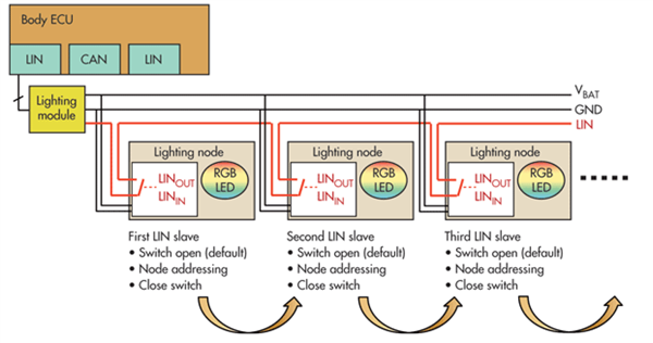
Figure 3 – Automotive Interior Ambient Lighting Configuration
In summary, color is everywhere and understanding color’s effect is important. The effective control of an RGB device is highly complex but simplified by modern electronics and color space charts. As a light source the LED is efficient, highly practical and widely used to make our world more colorful and “greener” - a color that our eyes are most sensitive to and one that resonates with planet earth.
For more information on driving automotive LEDs or to start a design, visit www.ti.com/autoled.
↧
↧
Free Webinar From TI and Nuvation: Green Power Grid - Connect, Control and Communicate
As the “electricity grid” evolves into the “smart grid,” energy management needs are increasing in complexity. Innovations such as integrating renewable energy sources, smart meters, electric vehicles and large-scale energy storage systems into the grid promise important rewards while also driving design complexity.
With the accelerated pace of such changes, how do you make sense of all this and build designs that are scalable and adaptable?
For the answers to these questions and many more, join Nuvation Engineering and Texas Instruments on March 19 at 11:00 am PST / 2:00 pm EST for a free webinar entitled “Green Power Grid: Measure, Control, Communicate.”
Join Smart Grid electronic design experts for an exciting discussion examining:
- A brief overview of the evolution of the smart grid
- Addressing efficiency and reliability of the grid on a global scale
- The challenges of integrating renewable energy sources
- A case study of an energy storage management solution from Nuvation Engineering that addresses a critical renewable energy integration issue
Speakers:
Stefan Janhunen
Senior Design Engineer, Nuvation Engineering
Punya Prakash
Business Manager, Industrial & Energy Automation, Texas Instruments
Moderator:
Joseph Xavier
Marketing Manager, Nuvation Engineering
Register Today!
http://www.nuvation.com/nuvation-texas-instruments-smart-grid-webinar#ixzz3Ry7hEmP7
↧
Simplifying merging units - Measuring a large numbers of currents and voltages in a “smart grid”
The “smarts” in a smart grid come from the ability the grid has to measure, control and communicate. Once a measurement is done, communication between the power distribution company and the customer creates an automated and widely-distributed electricity network that can protect, monitor, and optimize the operation of the interconnected components. This new automated network allows for utility companies to respond more efficiently to customer demand, and enables consumers to take more control over their energy usage through increased access to information.
In today’s complex power grid, the number of channels of currents and voltages that need to be monitored or measured are increasing dramatically. One of the challenges that directly flow from this is how to handle the large number of analog inputs coming in and then even after digitizing the signal how to get it into the processor without overwhelming the processor interface.
A merging unit is the interface from the physical analog world to the digital world using communication networks. The analog signal is converted to a digital signal and transmitted through -Ethernet network based on IEC 61850-9-2 (sampled values) communication protocol.
The TI reference design for the analog front end (AFE) for merging units (TIDA-00307) shows how multiple channels (8 at a time) can be modularly added to increase signal handling by adding additional successive-approximation-register (SAR) analog to digital converters (ADCs).

Multiple ADCs can then be connected together by using the daisy chain feature available on the SPI on the ADC, thereby minimizing the connectivity overhead from multiple ADCs to the controller.
The ADS8688 SAR ADC used in the reference design operates at a throughput of 500 kSPS. The device features integrated analog front-end circuitry for each input channel with overvoltage protection up to ±20 V, an 8-channel multiplexer with automatic and manual scanning modes, and an on-chip 4.096-V reference with extremely low drift. Operating on a single analog supply of 5 V, each input channel on the device can support true bipolar input ranges of ±2.56 V, ±5.12 V and ±10.24 V.
The device also offers second-order antialiasing filter, ADC driver amplifier and an extended industrial-temperature range. Additionally, this solution enables simultaneous sampling. When two devices are connected in daisy chain and the same chip selected is asserted for sampling, sampling delay will be minimal between the CH0 of ADC1 and CH0 of ADC2.
This solution from TI shows how a merging unit can not only be designed in a modular fashion, which enables the easy increase in channels as needed, but also how to interface the ADC to the processor without overloading the processor’s interface. In addition, this solution is not only compact with a high level of integration but it also allows simultaneous sampling when using multiple ADCs.
More information can be found here in the TI Design library: TIDA-00307
↧
DIY with TI: Engineer makes magic with time-lapse photography system
At TI, we celebrate the makers and hobbyists who enjoy creating and innovating on their own time. In our ongoing DIY with TI series, we share their incredible Do It Yourself inventions using TI technology.
 Thorsten Lorenzen is making magic with his DIY know-how.
And he is doing it in his spare time in a workshop attached to his house in Munich, Germany.
The wheels started turning last year when his longtime friend and professional photographer, Maik, asked Thorsten if he could build a contraption that could help him enter the time-lapse photography market. Thorsten agreed to build a time-lapse photography system for fun.
“I have always loved building small embedded systems. It was exciting to build this system from ground up, including the specifications, concept layout, mechanics, PCB design, soldering, programming and testing,” he said. “Working on fascinating systems such as this one enhances my life.”
Wheels in motion
Thorsten started the project by constructing a mechanical slider. He incorporated our DRV8412-C2 motor driver, mounted a camera on the slider and programmed it to run several moving sequences. The motor driver allows the camera to stop in precise positions as it moves along the slider.
He also incorporated a C2000 processor and built a controller that triggers the camera to take photos at certain positions along the way.
“There is no way for time lapse to record without a mechanical system,” he said. “It’s much more constant than someone taking the photos, and it is fully automated.”  Thorsten said his photographer friend was amazed at what could be done using modern technologies compared with low-cost systems found on the market.
“In particular, he loves the programmability of the system, which allows many different scenarios to be set. He sees the opportunities the system enables for entering new markets,” Thorsten said. “In today’s markets, photos and video clips for commercial reasons such as product placements need to be more exiting to make them attractive for customers and consumers. More motion creates more emotions."
About Thorsten
Thorsten has worked at TI for five years and is a senior field application engineer (FAE) for the Automotive Advanced Driver Assistance Systems (ADAS) business in Europe. He works with vision-based DSP systems and consults with customers. Because he routinely travels for his job, he has very limited time for DIYing in his workshop at home.
“This turned out to be a great opportunity to feel like a customer to TI. I haven’t worked with motor control at TI at all,” he said. “I got to experience how customers feel starting a brand-new project with TI products. The experience was great.”
↧
↧
LaunchPad brings new era of control to FRC robots
This year’s FIRST® (For Inspiration and Recognition of Science and Technology) Dallas regional kick off was a mixture of excitement and determination as students received their kit of parts – which included the components they will need to build their robot for this year’s competition. For the first time this year, their kit included TI’s MSP430 MCU LaunchPad. The Launchpad is part of the custom I/O portion of the new control system launched by FIRST and will be used like a gamepad to give teams more fine-tuned control over their robots.
The robots built by FRC (FIRST Robotics competition) students can often be quite complex, and difficult to control effectively at competition. Often times, teams will use off the shelf gamepads and controllers, but the inputs on these are made for video games, not robots. Mapping a command like “elevator up” to the ‘Y’ button isn’t instantly intuitive unless the students have had a lot of time to practice. Rather than embedding in controllers for their robot, many teams build custom button interfaces so they can lay out inputs in a logical way for their specific robot’s actions. This greatly reduces stress on drivers, and makes it easier to learn on. To accomplish this, teams have used a variety of solutions, but most are either far too complex or too limited in what they can do.
To this end, we created the LaunchPad USB GamePad software and associated utility. This lets teams easily select a prebuilt configuration that matches their needs, with plenty of input options available. Once programed, the LaunchPad shows up in the FRC driver’s software just like any other controller, making it very easy to interface with in their robot software. For the teams that still decide to use an off the shelf gamepad, they can still use the LaunchPad to run smart LEDs on their robot (a very popular addition), aggregate sensor data, or tap into the wide variety of Booster Packs available to learn embedded electronics.
(Please visit the site to view this video)
The students working on these robots are already building amazing things, and with TI’s help, they really push the limits of not only their robot, but their education as well. To get you jumpstarted using your LaunchPad, check out this wiki page we developed that has example code and three specific demos of how teams can use the Launchpad in this year’s FIRST competition. This is a great starting place for any student looking for technical information on how to most effectively use the LaunchPad.
Best of luck to all you future innovators!
↧
SAR ADC response times: Interface topology makes a difference (Part 3)
In Part 2 of this series, I explained a serial interface in which a conversion result for sample S is transferred to the host controller after the conversion is complete but before the start of the next conversion. I also noted that with this type of interface, both the throughput and response time of the analog-to-digital converter (ADC) degrade when using lower clock speeds.(read more)![]()
↧
Happy National Battery Day
Let’s get this party started! Celebrating National Battery Day on February 18. We all know Ohm’s famous law, V = IR. But before that, Alessandro Volta figured out that Q = CV. He was born on Feb. 18, 1745, and among his many great achievements was the development of the first practical battery in the late 1700's. (read more)![]()
↧
What are you sensing? Active shielding for capacitive sensing, part 1
Have you been experiencing problems with fluctuations in capacitance measurements within your sensor system? There are several explanations for these fluctuations, but the most common root cause is external parasitic capacitance interference. This interference, for example unintentional hand proximity or EMI from the surrounding area, requires attention and should be addressed in system design, since it can significantly reduce system reliability and sensitivity. Fortunately, there are ways to help mitigate these factors so that they do not affect capacitance-measurement readings; one of those ways is through active shielding. The FDC1004 features active shield drivers that can reduce interference and help focus the sensing field of a capacitive sensor.
Imagine a wire connected to one of the channel inputs of the FDC1004. As your hand approaches the wire and comes into contact with it, your hand forms a closed loop with the signal on the wire, since the human body acts as a grounded source. If your hand is not the intended target, it is considered a parasitic capacitance. The solution: an active shield wrapped around the wire. The shield driver is an active signal output that is driven at the same voltage potential (same waveform) as the sensor input, so there is no potential difference – and thus no capacitance – between the shield and sensor input. Any external interference will couple the shield signal with minimal interaction with the sensor signal. Figure 1 shows how shielding the signal line from sensor to the FDC1004 will reduce any interferers from affecting capacitance measurements.
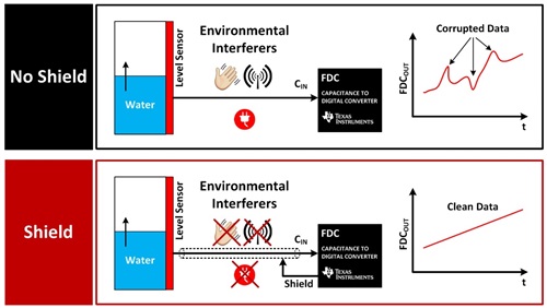
Figure 1: Shield versus no shield comparison
There are several benefits to using a shield in capacitive-sensing applications:
- It directs and focuses the sensing zone to a particular area.
- It reduces and eliminates parasitic capacitances and interferers.
- It eliminates temperature variation effects on the ground plane.
Directivity with a shield
With no shield, the sensor, CH, detects objects above and below the sensor. Depending on the application, detection above and below may not be acceptable and can misrepresent the capacitance measurements relative to a target. By using a shield sensor underneath the CH and GND electrodes, the field lines below are essentially blocked; only the top field lines have a defined path. The example shown in Figure 2 is somewhat simplified and does not include fringing effects.
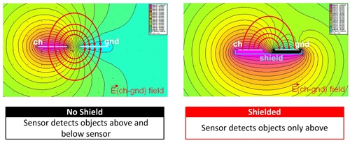
Figure 2: Electric field lines between CH and GND
Parasitic capacitance and interferers
Good system-level design principles require a ground plane to help reduce noise and increase signal integrity. For capacitive-sensing applications, a ground plane becomes an issue because it creates a termination source for electric field lines, even though the ground plane is not where the intended sensing area should be. If the printed circuit board (PCB) stack up is similar to that shown in Figure 3, fringing effects will occur and cause the measurements to include the capacitance path from the sensor to the ground plane. This large ground parasitic capacitance can be reduced significantly with a shield plane between the sensor and ground plane.
In an ideal case, the shield will eliminate all influence from the ground plane; but because of fringing effects, a small parasitic ground capacitance amount will still exist in the measurements. The shield size would have to be much greater than the size of the sensor and ground plane so that the field lines on the edges are much weaker compared to the overall capacitance measurement.
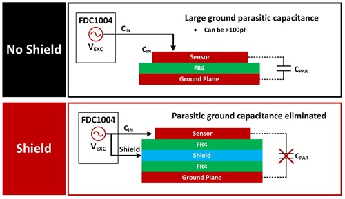
Figure 3: Ground-plane effects with and without shielding
Temperature effects on ground planes
Temperature is a factor that causes the parasitic ground plane capacitance to vary in addition to the initial parasitic capacitance offset it introduces into the measurements. This is seen as an offset that is time-varying. These variations from temperature are caused by expansion and contraction of the ground plane. Inserting a shield plane between the sensor and ground plane helps mitigate the influence of the parasitic ground plane capacitance from the measurements.
Typical implementation with the FDC1004
The FDC1004 has the capability to drive a 400pF load on the shield driver pins. Any load greater than 400pF will cause the shield to not function properly and effectively. Pairing the input channels with a shield depends on the mode of operation. In single-ended mode, CIN1 through CIN4 can be paired with either SHLD1 or SHLD2, because the two shield pins are shorted internally. For differential mode, Table 1 lists the in-phase conditions.
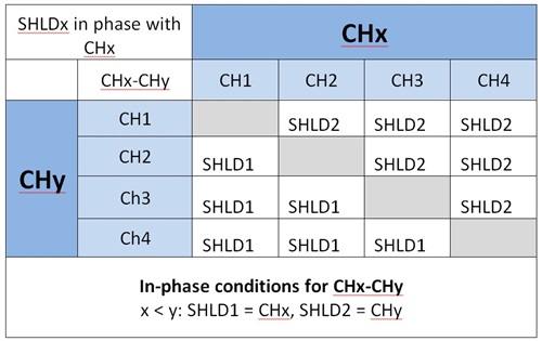
Table 1: Channel and shield pairing for differential mode
For example, if the FDC1004 is configured so that CH1-CH4, CH1 would be in-phase and paired with SHLD1, while CH4 would be in-phase and paired with SHLD2.
Stay tuned for part 2 of this series to learn more about shield sensor design, and how the size and placement of the shield in relation to the sensor electrode affects sensor performance.
Additional resources:
- Download the FDC1004 data sheet.
- Experience capacitive-sensing technology firsthand with the FDC1004EVM, which you can order today for US$29.
- Check out the newest TI Designs reference design for capacitive-based human-proximity detection for system wake-up and interrupt.
- Search for answers and get help with your designs in the TI E2E™ Community Capacitive Sensing forum.
↧
↧
Making safety systems safer with the right LDO
Making safety systems safer with the right LDO
When it comes to safety, most everyone is willing to pay top dollar. This is especially true in the world of automobiles, where fast moving objects have the capacity to turn into destructive weapons in an instant. Luckily, with the advent of faster, more precise electronics, cars have become safer as a result. One needs only to look at advanced driver assistance systems (ADAS), which aid drivers through various maneuvers and help avoid accidents. Of course, the element of human error cannot be entirely eliminated from the act of driving, but it can be mitigated through technologies like ADAS.
Much of the safety that ADAS boasts is contingent upon the dynamic, external data the system is constantly gathering and making decisions with. Take an ADAS radar system, for instance. Long-range radar is used for adaptive cruise control, while short-range radar is used for blind-spot collision, rear-collision warning, lane-change assist, and a few other functions, as shown in figure 1. Both radar systems rely on precise signal processing to ensure proper operation. The proper signal-conditioning integrated circuits (ICs) are imperative for providing the best data to the digital signal processor (DSP). However, even after carefully choosing the right devices, there’s always the problem with noise.

Figure 1: ADAS systems
For this blog post we are focusing on the noise that propagates through the power supply rails and has the capacity to compromise the signal. Of course, power supply noise cannot always be isolated to a single source, but one common culprit is the switched-mode power supply. Ripple current generated via switching (see Figure 2) has the potential to compromise sensitive signals via the supply rails of the various subsystems. (This is a necessary evil, as a switched-mode power supply (SMPS) is required to efficiently step down from the 12V battery to 5V.) Ripple, isolated at a certain frequency and its associated harmonics, is one element of power supply noise. The other element is the noise spread over a broad frequency spectrum expressed in terms of a root mean square (RMS) value. Both elements of noise have the capacity to adversely affect signal integrity.

Figure 2: Output ripple in continuous conduction mode (CCM) for a 60V, 3.5A automotive-qualified DC/DC converter
Within radar systems, phase-locked loops (PLLs), precision clocks, monolithic microwave integrated circuits (MMICs), jitter cleaners, and other radio frequency (RF) circuitry are especially susceptible to power supply noise. Power supply noise increases phase noise in PLLs and clocks and generates corresponding jitter. Jitter cleaners can help correct this, but they too can be susceptible to ripple on the supply rail. MMIC data sheets often spec a minimum ripple requirement and it is generally good practice to minimize noise on data converters to ensure the highest bit resolution.
As shown in Figure 2, the ripple voltage coming off the DC/DC converter is ~10mVpp occurring at ~500kHz. Although that noise value may not be problematic in some applications, systems such as radar applications require the best signal-to-noise ratio (SNR) to ensure optimal performance. As such, a low-dropout regulator (LDO) is needed. The TPS7A8101-Q1 and TPS71701-Q1 have high power-supply rejection (PSR) and can attenuate this ripple voltage tremendously. Take a look at Figure 3, which is the power supply rejection ratio (PSRR) curve for the TPS7A8101-Q1.
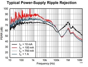
Figure 3: Typical PSRR for TPS7A8101-Q1
At 500kHz, the PSRR is approximately 57dB. This will attenuate any 500kHz signal by a factor of over 700. Consequently, the 10mVpp ripple becomes a ~14μVpp ripple. This effectively eliminates any chance of switching noise affecting the signal through the supply rails.
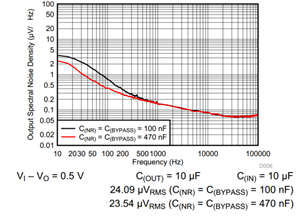
Figure 4: Output spectral noise of TPS7A8101-Q1
Additionally, the TPS7A8101-Q1 has low output noise, as shown in Figure 4. The low RMS value ensures that the noise floor for the various ICs does not increase, thus preserving SNR.
Both high PSR and low output noise are integral to making sure that power supply noise is not afflicting signal integrity. LDOs are effective means of filtering switching noise and providing a clean DC output. As a result, signal processing ICs operate as they are meant to – without any compromise. This ultimately translates to the reliability of the radar system, which will become more integral to driver safety as technology advances. “Safety first” remains as important as ever; low-noise LDOs are a means of helping to achieve that.
For more information about LDOs visit these resources:
↧
ADC power-supply rejection, calculating allowed supply ripple
In my previous blog, “Measuring PSRR in an ADC,” I looked at the methodology and techniques needed to measure the power-supply rejection ratio (PSRR). In this blog post, we’ll finish the analog-to-digital converter (ADC) characterization, interpret the results, and look in-depth at component selections to understand power-supply specification trade-offs versus ADC performance.
Let’s first start by looking at the ADC PSRR characterization. For continuity, we’ll use the ADC3444 as the example. The ADC3444 is a quad, 14-bit, 125MSPS pipeline ADC. Using the methodology developed in “Measuring PSRR in an ADC,” we created these PSRR plots:
- Analog VDD (AVDD) PSRR at DC and around fundamental versus frequency.
- AVDD PSRR versus fundamental input power.
- Digital VDD (DVDD) PSRR versus frequency.
As a reminder from the previous discussion, the AC signal of frequency f0 inserted in the ADC analog power supply (AVDD) is generating three spurs: one at DC at f0 and two around the single tone, at frequencies f ± f0. The same AC signal on the digital power supply of the ADC (DVDD) is at f0. See Figure 1.

Figure 1: Spurs location due to an AC signal present on the ADC power supply
The ADC3444 AVDD and DVDD supplies full PSRR characterization, as shown below. Note that the local bypass to each ADC was in place, with 0.1µF on each AVDD supply pin and 0.22µF on each DVDD supply pin, for a total of 1.3µF on AVDD and 0.88µF on DVDD. Figure 2 is the test configuration block diagram.

Figure 2: (a) AVDD test circuit configuration; (b) DVDD test circuit configuration
Figure 3 shows the PSRR versus frequency for a fundamental at -2dBFS. Two conclusions jump out at you:
- The PSRR for the two spurs around the fundamental is 20dB worse than the PSRR at DC.
- Both PSRRs are flat to ~200kHz and are actually improving.
The worsening PSRR around the fundamental could suggest a dependency to the fundamental amplitude. So I measured the PSRR versus amplitude fundamental with a 500kHz ADC-supply AC signal (disturber signal).
The PSRR improvement versus frequency is not caused by the ADC PSRR, but by the disturber signal being attenuated by the bypass capacitors.

Figure 3: AVDD PSRR vs. frequency
To verify that the PSRR of the AVDD supply is dependent on the fundamental, Figure 4 was measured. It shows a dB/dB dependency of the spur with the fundamental. In other terms, the disturber is present around the fundamental with a set dBc (dB below carrier) response. At DC, the disturber stays constant for any signal in the dynamic range of the ADC.

Figure 4: AVDD PSRR versus analog input power
I took the same approach for the digital power supply of the ADC, reflected in Figures 5 and 6. As expected, the digital-supply PSRR is much better than that of the analog supply by one order of magnitude, or 20dB. The presence of the bypass capacitor is also felt, but beyond 300kHz but does not last as long as on the analog supply. There is also no dependency on the amplitude of the fundamental.

Figure 5: DVDD PSRR versus frequency

Figure 6: DVDD PSRR versus input power
This was an interesting exercise, but what conclusion can we draw from the results?
The first conclusion is that the architecture used in the ADC3444 is as mostly sensitive on the analog power supply. Keep in mind that the above results are typical and a guardband should be added. Since 28dB is the worst result at -2dBFS and the PSRR is degraded dB/dB, the full-swing 0dBFS would have 26dB PSRR. Consider a guardband of at least 10dB for overtemperature and overprocess variations, leaving the minimum PSRR for the ADC3444 AVDD to be 16dB. The 10dB guardband is an estimate and requires additional characterization to ensure an adequate performance level.
Using the same equations as those found in “Measuring PSRR in an ADC,” see Equations 1 and 2 below. It is now possible to estimate the maximum allowable ripple present at the DC/DC converter, considering for now that the ADC is powered directly from a supply that contains ripples.

Figure 7: Circuit configuration for a non-ideal AVDD supply
The system design tolerance will reveal the maximum acceptable spur to maintain the desired performance. Let’s consider here that the worst spur cannot exceed -95dBFS. This means that with a 16dB worst-case PSRR and using Equations 1 and 2 below, we can determine the maximum allowable power-supply ripple.

 (maximum allowable ripple amplitude after ADC PSRR attenuation)

This leads us to:

This is the maximum ripple that can be present on the AVDD power-supply pin.
We can loosen this stringent requirement by:
- Reducing the guardband on the PSRR.
- Not operating the ADC at full dynamic range.
- Allowing spurs greater than -95dBFS in the FTT.
The DVDD supply PSRR would have the test configuration shown in Figure 8.

Figure 8: Circuit configuration for a non-ideal AVDD supply
The DVDD is worst at 62dB. Maintaining a 10dB margin on this typical value, we can calculate that the worst disturber on the DVDD supply pin to ensure -95dBFS performance in the FFT is 14.17mVpp.
These calculations provide a guideline for the required performance of both power supplies for the ADC. In my next post, I’ll discuss developing an adequate power-supply solution for each supply and its impact on performance.
Additional Resources:
- Download an evaluation module of the ADC3444.
- Check out the latest data sheet for TI's TPS7A401 LDO family.
- Complete portfolio of linear dropout regulators (LDOs)
↧
Industrial communication solutions with MSP430 MCUs
 When it comes to factory automation, developers can either use wired or wireless communication interfaces to carry the data back from the digital-to-analog converter (DAC) to the amplifier to complete the loop. The wired interfaces are more commonly used, which include the 4-20mA, HART and IO-Link. TI's ultra-low-power MSP430 microcontrollers also play an important role of control and datalogging in industrial transmitter applications, especially in loop-powered applications where ultra low power is a key differentiator.
The most popular communication interface for factory automation is the 4-20 mA current loop, a very robust sensor signaling standard. Current loops are ideal for data transmission because of their inherent insensitivity to electrical noise. As mentioned earlier, the transmitter can either be powered through the communication loop via a 2-wire implementation or through a separate power line not associated directly with the 4-20mA current loop, typically classified as a 3-wire or 4-wire solution.
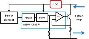
The single-chip MSP430 system solution has integrated smart analog. The on-board operational-amplifier (op-amp) can be configured to carry out signal conditioning of the sensor signal and drive the 4-20mA communication loop. This single-chip solution drives the most cost effective solution for developers.
TI Design: TIDA-00247
The other communication protocol for industrial applications is the IO-Link which is known as the USB of factory automation since it is a simple and cheap point-to-point protocol that reuses the cables and connectors from an installed base of industrial sensors and actuators, leveraging existing wired infrastructure.
 The IO-Link MSP solution serves as a full turnkey IO-link sensor evaluation and fast prototyping platform. It has an MSP430 FRAM microcontroller enabling easy, fast and secure sensor configuration updates and reduces overall power. It also supports sensing break-away and hence, can be removed to connect any analog sensor.
The HART communications protocol is a digital industrial automation protocol. It’s most notable advantage is that it can communicate over legacy 4-20 mA analog instrumentation wiring. Thus, the HART protocol is gaining popularity since it has made a good transition protocol for users who are comfortable using the legacy 4-20 mA signals, but want to implement a "smart" protocol.
 MSP430 MCUs directly support the PHY layer in the HART communication solution, which removes the need for an external HART modem IC. It is based on MSP430F5529 and MSP430FR5969 LaunchPad evaluation kits and a modular BoosterPack solution that provides easy prototyping and the ability for customization of the signal conditioning and sensor setup.
↧
TI Design: EtherCAT & EnDAT enabling Industrial Single chip drive
The AM437x platform enables deterministic Industrial Ethernet and high precision feedback interface through the quad core Programmable Real-time Unit (PRU) or Industrial Communications Sub-system (ICSS). The TI Design for a single chip drive on Sitara processors combines EtherCAT and EnDat and provides designers with a single solution that allows for motor control and higher communication standards. The conformance was tested by the highest standards of the EtherCAT Technology Group (ETG), ensuring a high quality Industrial Ethernet performance. The combination of EtherCAT and EnDat 2.2 into one chip significantly decreases system costs and allows developers more integration between products.

Based on the HEIDENHAIN EnDat 2.2 standard, this TI Design enacts a hardware interface solution for position or rotary encoders. The platform of this design is also compatible with a broad range of industrial automation equipment, allowing designers to execute real-time EtherCAT communications standards. The single chip drive enables designers with a low power solution to use in applications such as industrial automation, factory automation, or industrial communication.
The industrial software development kit for the Single Chip Drive processors AM4377 and AM4379 includes Certified* EtherCAT firmware with free ETG membership, and board support package to jump start your design. Order your board today here.
For more information on EtherCAT on Sitara processors, read this white paper.
*Firmware certified on primary development platform only
↧
↧
Save money when you buy MSP430 FRAM LaunchPad Bundles
Start your microcontroller projects today with more than 30 percent offMSP430 FRAM MCU LaunchPad bundles on the TI Store:


MSP-BNDL-FR4133IR: MSP430FR4133 LaunchPad Development Kit with Infrared (IR) BoosterPack Plug-in Module Bundle
Turn your MSP430FR4133 LaunchPad into a universal remote control by leveraging the keypad and IR transceiver on the Boost-IR.
Now only $17.99! (no coupon required)
MSP-BNDL-FR5969LCD: MSP430FR5969 LaunchPad Development Kit with Sharp® Memory LCD BoosterPack Plug-in Module Bundle
Add high-contrast images or text output from your MSP430FR5969 using this 96x96 pixel LCD from Sharp.
Now only $24.50! (no coupon required)
These promotional prices will be available through the end of the month, so head over to the TI Store to get started today!
↧
When STEM first stole my heart…
On Monday, engineers all over the United States begin their celebration of National Engineers Week. The annual event, started by the National Society of Professional Engineers more than 60 years ago, is designed to encourage a diverse future engineering...(read more)![]()
↧
Exploring the MSP430 tool chain: Part 3 – Programming with the MSP430 Bootstrap Loader (BSL)
This is the third entry of a five-part series to help you learn more about our robust MSP430 MCU tool chain. Don’t miss Parts 1 and 2 on this blog from past weeks, because this week we focus on MSP430 target boards.
The MSP430™ Bootstrap Loader (BSL) is a program built into each MSP430 microcontroller for the purpose of reading and writing to memory via UART or USB. It enables users to communicate with embedded memory in the MSP430 device during the prototyping phase, final production and in service. Both the programmable memory (flash memory) and the data memory (RAM) can be modified as required.
The Bootstrap Loader can be divided into two major types: ROM-based BSLs found in the MSP430F1x/2x/4x and FR2x/4x/5x/6x families, and flash-based BSLs found in MSP430F5x and F6x devices. Though similar, both BSLs have a different protocol and command structure. In addition, the flash-based BSLs can be overwritten with a new program, for instance a BSL which communicates via I2C. If the device is secured by disabling JTAG, it is still possible to use the BSL. Access to the MSP430 memory via BSLs is protected against misuse by a user-defined password.

Have you ever heard of the MSP430 MCUBSL tool (known as the "BSL Rocket")? It is a low-cost programmer for MSP430 MCUs designed to allow communication to MSP430 BSLs via Virtual COM ports. It is completely open source and the firmware can be compiled and run on either TI Target Socket Boards, or third-party produced boards. The programming adapter is compatible to all existing MSP430F5x/6x devices which feature a UART or I2C BSL firmware. Click here for how to get started and click here to learn how to use BSL Rocket with our MSP430F1x/F2x/G2x/F4x devices.
 In order to make communication with the BSL easier, TI released the MSPBSL_Library as an Open Source Project on Github. This library is a project that is designed to allow developers to create PC-side applications for Windows, Linux and Mac OS without having to focus on lower-level communication layers. This library encapsulates all the complexity of communication behind an easy-to-use API with being cross platform and object oriented.
For more information, check out this helpful documentation below:
- MSP430 Programming Via the Bootstrap Loader User’s Guide
- MSP430FR57xx, MSP430FR58xx, MSP430FR59xx, MSP430FR68xx, and MSP430FR69xx Bootstrap Loader (BSL)
- MSP430FR4xx and MSP430FR2xx Bootstrap Loader (BSL)
- Creating a Custom Flash-Based Bootstrap Loader (BSL)
- MSPBoot – Main Memory Bootloader for MSP430 Microcontrollers
↧
Power Tips: Solar panel lighting requires a system-level approach
Going green isn't always quite as simple as it seems; for example, take a system designed to store solar energy in a battery to power light-emitting diodes (LEDs) at night. As you can see from the block diagram (Figure 1), this system involves much more than just a battery and LEDs. The design can be broken up into multiple sub-functions, each requiring careful consideration at a system level. Let’s review these sub-functions.
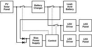
Figure 1: Solar-powered LED lighting system
Control algorithm
Simply connecting the (50W/21V) solar panel across a 12-V battery (through a diode) sacrifices about 30 percent of the available solar energy to charge the battery. This is due to the current-voltage characteristics of solar cells. When the panel is lightly loaded, its output voltage remains high, only drooping slightly as the load on it increases. When loaded beyond its maximum output power, the panel’s voltage rapidly collapses.
It is desirable to continuously operate at the panel’s “knee,” thereby extracting the maximum power under all lighting conditions. This is known as maximum power-point tracking (MPPT), but can be difficult to achieve because it changes with solar intensity, temperature and changing environmental conditions. Many MPPT control algorithms exist, with the most effective requiring microprocessors.
A simple, less-accurate method simply loads the panel to 76 percent of its open circuit voltage to approximate MPPT. But with the total cost of using solar panels still high, microprocessor control is recommended, as wasting energy isn’t a good option.
Battery charger
Each battery technology requires an optimized charging strategy to maximize capacity and life. Lead-acid or absorption glass mat (AGM) batteries offer high capacity at a low cost per amp-hour compared to other chemistries. The charger must have circuitry to precisely measure the charging current, as this is part of the data necessary for MPPT. All available solar-panel current is stored in the battery until it reaches its maximum charge voltage, at which point trickle charging begins. The battery must be maintained at the proper float voltage, which should be adjusted with a negative temperature coefficient. This necessitates additional circuitry to monitor the battery’s temperature, or at minimum the ambient temperature. If not implemented correctly, overcharging is possible and damage to the battery may occur.
Bias supply
Whether you’re using a microprocessor or analog circuitry, you’ll probably need a bias supply to power everything. You can use the solar panel and/or the battery as the input source, but you’ll have to consider various topologies depending on the expected minimum and maximum input voltages. A single-ended primary-inductor converter (SEPIC) or synchronous buck converter would likely cover most situations. Avoid less-efficient converters such as traditional bucks and linear regulators. This is not a system where you should be wasting power.
LED driver
Finally, the LEDs get to burn all of the efficiently gathered power. But they should burn it efficiently! Since it’s likely that multiple LEDs will be involved, a boost converter is the topology of choice when operating from a 12V battery. LEDs are typically driven with a constant current, so you must configure the boost converter as a current regulator. This provides constant illumination, even as the battery voltage decreases.
Finally, control logic is necessary to determine what the system should be doing at all times. These states include bulk battery charge, trickle charge, battery overvoltage/undervoltage, solar-panel connect, LED on/off, battery temperature control, etc. All of these functions must work seamlessly together and must be designed as a whole.
If you are interested in the trade-offs and intricacies involved in a solar lighting system, additional detail can be found in: Power Supply Design Seminar SEM1900, topic No. 7, “Designing a Solar-Cell-Driven LED Outdoor Lighting System.”
↧
↧
Start your BLDC journey with motor startup (Part III): Initial position detection (IPD)
In part I and part II of this blog series, we talked about ‘blind’ startup of a motor, which is an easy approach but has certain limitations. If the application can’t accept the blades going back and forth (as in ceiling or pedestal fans) or reverse spinning is prohibited (for example HDD motor or VCM), you should consider initial position detection (IPD).
IPD is the method to detect the motor position before it spins up. Because back electromotive force (BEMF) related methods are not available before the motor starts, we need to find another motor characteristic that is a function of motor position. Motor winding inductance (saturation) meets this requirement.
The equivalent circuit of the motor winding is an inductor in serial with a resistor. The magnetic field in the winding increases when the phase is driven with current.

The material of the winding core, the silicon steel, has a saturation point where the magnetic field can’t increase as fast as the current increase. The saturation point is determined by the magnetization curve (BH curve) of the substance.

The permanent magnet of the brushless DC (BLDC) motor generates a magnetic field in the winding core that can superimpose to the magnetic field generated by phase current.

Here is a simple experiment to verify this principle:
1) Turn on the switch. The 12V power supply starts to charge the inductor.
2) Turn off the switch when the inductor current reaches 1.6A.
3) Capture the current waveform.
4) Put a permanent magnet close to the inductor.
5) Provide an extra magnetic field to the inductor core.
6) Repeat the test.


Here is the result:
With the magnet nearby, the inductor is saturated and the current increases faster.

Also, the stronger permanent magnet we choose, the shorter time the current reaches the threshold.

We can apply this concept to the motor.
Sequentially apply voltage across two of the three motor phases this way: VW WV UV VU WU UW. When the current reaches the threshold, the voltage across the motor is stopped. Measure the time it takes from when the voltage is applied until the current threshold is reached. The time varies as a function of the inductance in the motor windings.

The state with the shortest time represents the state with the minimum inductance. The minimum inductance is because of the alignment of the north pole of the motor with this particular driving state.
In order to achieve an accurate IPD result, several parameters should be properly selected.
1. IPD current threshold
2. IPD clock
3. IPD release mode
Please refer to DRV10983 datasheet and DRV10983 turning guide to learn more about the IPD parameter selection.
Does this answer all of your questions on how to start-up your BLDC? What other BLDC questions can I answer?
↧
Industrial DACs: How to protect 2-wire transmitters
In my previous post, I explained how to design 2-wire, or loop-powered, analog outputs for industrial automation. In this post, with the design and operation of the transmitter in mind, I will talk about how to design circuits to protect these systems. For reference, Figure 1 shows the basic 2-wire transmitter design.(read more)![]()
↧
How to do a BOM review for a low-power DC/DC converter design
When reviewing a design, a schematic review is very common and important. Simple errors and omissions can be caught just by having someone, besides the circuit designer,—check the design. (read more)![]()
↧