Quantcast
Channel: TI E2E support forums
Viewing all 4543 articles
Browse latest View live

How to build a simple regulated positive and negative split supply

$
0
0

Creating a split supply that delivers both a positive and negative voltage to the system has always been a pain on a good day for most of us. Some systems use push-pull transformers. Others use a boost converter with an AC-coupled output to create a positive and negative rail. But both choices have serious challenges and may add cost, size and complexity that you cannot afford in your design – especially if your design is for a small form-factor application.

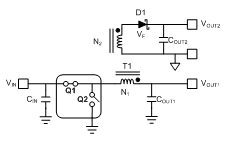
The push-pull method is traditionally used for high-power systems and is often just reused from previous designs. If built from scratch, its design is going to be complex and large, as you can see from the simplified schematic shown in Figure 1.

Figure 1: Push-pull method can produce complex and large designs

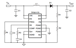
When using a boost converter (as shown in Figure 2’s simplified schematic), only the positive output is truly regulated, while the negative output goes along for the ride. And that negative voltage might not be very accurate.

Figure 2: In traditional Push-Pull method, the negative output goes  

along for the ride in the boost converter

 So what alternative exists for a simple and accurate bipolar split supply?

This family of split-rail converters from Texas Instruments is a superior alternative. It can help you build simple, cost-effective and regulated split supplies fast. A split-rail converter is a dual-output converter generating regulated positive and negative voltages from a single input rail. With one split-rail converter, you only need one device to generate both a positive and negative supply with one input rail.

The main advantages of TI split-rail converters are:

  • Regulated outputs.
  • Integrated solution/low bill of materials (BOM).
  • High-efficiency devices.

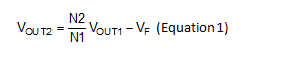
As you can see from the schematic in Figure 3 of the TPS65132, this split converter can generate a ±5.4V signal with a small footprint and a limited number of external components. The full voltage range of the device can be configured between ±4V & ±6V (asymmetrical or not).

Figure 3: The TPS65132 generates a ±5.4V signal with a small footprint and a limited number of external components

Split-rail converters are ideal for general dual-power-supply applications such as musical instruments, home audiovisual equipment, sensors, measurement equipment, medical equipment and more because they are flexible, simple and accurate. To help determine if split-rail converters could work on your next design, check out TIDA-00385 for powering headphone amplifiers.

In what applications could you use a regulated ± output?

Additional Resource:

Chris Glaser Fully Charged blog post, Killing two birds with one stone


How to protect USB host ports with ESD current-limit protection devices

$
0
0

One of the hottest topics regarding interface technology today is the universal serial bus (USB) Type-C connector, popular for its reversibility, higher data transfer, power delivery and additional protocols. While there is much excitement over the new standard, the reality is that the USB Type-A connector is still prominent and is being designed into end equipment today. When designing for USB host ports, you should consider two major areas of protection: overcurrent protection and electrostatic discharge (ESD) protection.

Overcurrent protection

Per section 7.2.1.2.1 of the USB 2.0 specification, “All host and self-powered hubs must implement overcurrent protection for safety reasons.” You can accomplish this by using a fuse or current-limit switch. Moreover, a current-limit switch is the preferred solution over a fuse because it allows you to allocate less power per port during design. In a transient event, the load switch limits the output current to a safe level by operating in constant current mode. A fuse will allow the current to rise above the maximum current level until it shuts off. Choosing a current-limit switch allows you to select a smaller DC/DC converter and inductor because the switch more accurately limits the current during an overcurrent event. The current-limit switch also allows for decreased Vdroop in the 5V Vbus during transients versus a fuse implementation.

ESD protection

When designing USB ports, you should be aware of the high risk for ESD strikes and consider using ESD protection to prevent damage. For example, USB controllers and transceivers often handle ESD ratings based on the human body model. This rating is the oldest and most commonly used to detect ESD sensitivity. The HBM rating is intended for chip-level ESD protection and does not guarantee that the system will be protected from higher level ESD strikes. The International Electrotechnical Commission (IEC) 61000-4-2 standard tests for higher levels of ESD energy when compared to the HBM rating, as shown in Figure 1. For system-level protection, consider selecting the more robust IEC 61000-4-2 standard and using a transient voltage suppressor (TVS) diode.

In USB 2.0 applications, system-level ESD protection should be considered for VBUS and the data lines. VBUS requires a large capacitor for handling power transients like hot-plugging, and therefore can pass IEC 61000-4-2 by means of the capacitor. However, the data lines require a different approach. The high-speed lines operate at a maximum data rate of 480 Mbps, which means a large capacitor cannot be added to protect from ESD. You will need a low-capacitance TVS diode in order to decrease the effect on signal integrity.

Figure 1: ESD test comparison

Complete solution

Traditionally, multiple devices met the protection requirements for a USB host: a current-limited load switch for Vbus plus one or more ESD protection devices for the data pins. The TPD3S014 combines a current-limit switch and two channels of ESD protection to make a single-chip USB host-port solution as shown in Figure 2. The TPD3S014 and TPD3S044 allow 0.5A and 1.5A of continuous current, respectively, in a space-saving 2.9 mm by 2.8 mm DBV package.

The current limits in this family feature reverse-current blocking and are Underwriters’ Laboratories (UL)-recognized components (UL2367). They also provide IEC 61000-4-2 (Level 4) ESD protection for the data pins. These devices simplify your designs by reducing the number of devices and shrinking the overall footprint of the printed circuit board (PCB) to ensure optimal USB host-port protection.

Figure 2: USB host-port protection solution

Additional resources:

Power over your Coax

$
0
0

Many smaller automotive electronic sub-systems receive their power from a coaxial cable.  This cable combines the power and data transmission to reduce the number of cables required.  This cable reduction decreases the extra weight and cost from the additional sub-system.  The numerous cameras appearing in new cars frequently use this “power over coax” scheme to deliver a few watts of power to the camera.

While the power sent over the coaxial cable is often protected from the battery’s extremely wide voltage excursions (3V to 60V, for example), a frequent challenge with power over coax is lesser voltage excursions produced by load changes and the subsequent voltage drop (IR drop) across the cable.  While the voltage at the Engine Control Unit (ECU) end of the cable might be regulated to 9V, the voltage at the camera end could be several volts different in either direction.  Supporting a wide input voltage range, such as 6V to 12V, and still delivering a well-regulated and low-noise output voltage is essential.

Since this camera sub-system is small and very low power, the power supply receiving the power over coax power should also be very small and highly integrated.  Due to the higher input voltage and small area available to dissipate heat, a linear regulator is not typically an option due to its low efficiency and high temperature rise at higher input voltages.

The new TPS62160-Q1, TPS62170-Q1 and TPS62172-Q1 fulfill this need.  These devices are very small, highly integrated, Q100 qualified, step-down converters supporting the wide input voltage range required for camera module applications.  Packaged in a 2-mm by 2-mm SON package and supporting a total solution size of less than 50 mm2, these devices convert a 3-V to 17-V input voltage down to a lower voltage rail to operate the entire sub-system. Over 90% efficiency keep the sub-system cooler--all the while making the best use of the limited power available.

What sub-systems are you powering with power over coax?

New approach for inrush current clamping with smart high side switch

$
0
0

Smart Power High Side Switch is the device with protection and diagnosis features, in which the system can easily realize the high reliability and intelligent fault detection. It’s widely used in automotive and industrial applications, for example, as a power switch for the rear view camera or the LCD screen in the infotainment system.   

One common design problem for these applications is the big inrush current, mostly derived from the abrupt low impedance in two scenarios: driving a big capacitive load or the hard short circuitry. To overcome this barrier, the pre-stage power margin, post-stage device stress, and the whole PCB traces and connector sizes should be carefully considered.

Nowadays, current limit function is implemented in most high side switches. The limit threshold is internally fixed due to the legacy of driving the high wattage bulbs in the automotive BCM system. For the other type of loads, the fixed value is too big for the clamping and protection. For example, some customers tend to use a 100mΩ RDSon device to drive an audio speaker amplifier module, in which the nominal current is only 1A but with 2 units of 470uF input cap.  For a traditional high side switch, the fixed current limit value is larger than 10A, so the inrush current increases up to 13A violently. This would create a big burden for the whole system design.

TI introduced a solution to help solve the inrush current trouble. The TPS1H100-Q1 is a fully protected high-side power switch, with integrated NMOS power FET and charge pump. Customers can easily set the current limit they want by connecting one external resistor to the CL (current limit) pin. The external resistor is used to convert a proportional load current into a voltage, which is compared with an internal reference voltage. When the voltage on CL pin exceeds the reference voltage, the current is clamped.


After the easy set-up, let’s show where amazing happens.

Scenario 1 --- Driving a big capacitive load.

Condition: Vs=13.5V. Start up with 470uF capacitive load.

Waveform benchmark: CH1 Input logic step from low to high, start-up signal. CH2 TI’s part, Output current with 1A current limit, 500mA/grid. CH3 competitors’ part, output current with internal current limit at 12A, 5A/grid.


Scenario 2 --- The hard short circuitry.

Condition: Vs=13.5V. Load: 5uH+100mohm (According to AECQ100-012 short to GND test condition).  Input control logic keeps high, and short to GND suddenly happens.

Waveform benchmark: Left Figure (Competitor’s Part): output inrush current on the competitors’ part. Right Figure (TPS1H100-Q1): Output inrush current on TI’s part.

Customers typically prefer the inrush current overshoot as low as possible and the response time as quick as possible. With the distinct device design, TPS1H100-Q1 can achieve much better performance both specifications. 

With this feature, the system can get much higher reliability to avoid big inrush current, while saving the cost of the preceding stage power supply and surrounding protection components. To learn more about this new approach to clamp the inrush current, check out the TPS1H100-Q1.

Connecting students with the International Space Station

$
0
0

Three-hundred and fifty students sat in complete silence in the auditorium at Council Rock High School South just outside of Philadelphia, Pennsylvania. The only sound heard was the constant static from the speakers hanging overhead. On stage sat three members of the K3DN.org amateur radio (ham radio) operating club, along with a science and astronomy teacher and 10 students anxiously awaiting a voice to cut through the crackling static.

TI Avatar“NA1-ISS, this is K3DN, can you hear me,” said one of the ham radio operators into the microphone.

Nothing but static.

“NA1-ISS, this is K3DN, do you read me,” the man repeated again.

Then, suddenly and faintly, a garbled voice could be heard.

“K3DN, this is NA1-ISS, I can hear you,” said Italian astronaut Samantha Cristoforetti, speaking from the International Space Station (ISS), traveling 220 miles above the auditorium and more than 17,000 miles per hour through space.

As soon as Samantha’s voice came through the speakers, you could see all of the high school students in the auditorium collectively lean forward in their chairs, but TIer Joe Horanzy couldn’t look up from his work area. The senior embedded processor field applications engineer and ham radio enthusiast sat busily at the controls of the radio system he built with two of his amateur radio colleagues, constantly switching dials and making adjustments to keep the space station tuned in for the eight minutes it was within range of his antennas.

“My heartbeat felt like I was running on a treadmill,” Joe said as he detailed the thrill of connecting with astronauts flying through space.

This momentous occasion, captured by local media (see the stories from CBS Philadelphia the Bucks County Courier Times), took weeks of planning and more than 150 volunteer hours by Joe and his ham radio operating friends.

Council Rock High School South has a unique relationship with the U.S. National Aeronautics and Space Administration (NASA). The high school participates in a number of NASA educational programs including building robots that NASA tested on their microgravity plane. Recently, NASA gave approval for the high school to communicate with the astronauts on the ISS. That was the easy part. The school then needed to find a way to make contact with the station as it hurdled through space in its orbit around Earth.

“Our mentor for this event lives in Toledo, Ohio and willingly donated $7,000 worth of equipment. All we had to do was pick it up,” said Jerry Fetter, an astronomy, meteorology and biology teacher at Council Rock High School South.

Jerry and one of his fellow teachers rented a truck and drove west to Ohio, packing up the equipment, which included a 12-foot antenna powerful enough to reach the ISS, along with a rotator to keep up with the station and all of the computer and other equipment to operate the system.

TI AvatarFrom there, the hard work began. The team bought 400 feet of cable with the connections and spent endless hours at the school installing the antennas (70 feet above the ground on the roof of the auditorium), laying cable, testing equipment and software and constantly problem solving.

“By the time we finished building, we had a little mission control just like in Houston, Texas,” Joe said with a smile.

The team worked out the last few bugs the day before the big event. As the students filed into the auditorium, a map displayed on the screen showing an X for the exact location of the ISS, with a small circle around it denoting the area in which the high school could communicate with the astronauts on board. Over the course of the next 30 minutes, the X traveled across the entire United States, and soon the outer edge of the communications circle hit the high school.

Less than 10 minutes and eight student questions later, the voice of the astronauts faded away, replaced by the static of their transmission.

“The neatest thing is providing kids with opportunities like this, real world moments exposing them to what it is like to be an engineer or to pursue a career in science, technology, engineering or math,” Jerry said. “This is what really inspires a kid – the stuff you just can’t teach in a classroom.”

With the successful connection to the ISS complete, perhaps the most rewarding part of the entire day followed. Students came up to Joe, wearing his TI polo shirt, to ask about his engineering work – and just how in the world (or out of this world) he was able to build, test and successfully run the system that connected them with astronauts flying high overhead.

“We talked about the science, technology, engineering and math, or STEM, making this event possible and how I use it every day in my job at TI,” Joe said. “And I told them if they study STEM subjects, get good grades and push themselves, there is a bright future with great career options.”

It took 150 hours of hard work and effort for just eight minutes of time with the astronauts. But the benefits of this endeavor will last well beyond that short connection.

And the award goes to…SimpleLink Wi-Fi CC3200

$
0
0

Written by: Kimberly Kulesh

We are excited that the SimpleLink™ Wi-Fi® CC3200 wireless MCU has been selected as the winner of several prestigious awards for industry excellence. As a part of the latest generation of the SimpleLink Wi-Fi family, this Internet-on a-chip™ solution allows developers to easily add wireless connectivity to their designs with no prior Wi-Fi experience. Here are examples of a few of our awards:

Electronic Products: 2014 Product of the Year

Starting the year off with a bang, Electronic Products selected the CC3200 as one of recipients of the 2014 Product of the Year awards. In the publication’s feature article about our Wi-Fi microcontroller, the CC3200 was praised for its low power performance, on chip crypto engine and the network processor offloading the MCU. All of these features make this single chip solution “wonderfully easy to integrate into an IoT system.”

Electronic Design: Best Communications Product of 2014

Continuing the momentum, Electronic Design released their Best of 2014 award winners, where the CC3200 was named the best communications product of the year. Electronic Design also published an article about the Wi-Fi chip, highlighting its Wi-Fi CERTIFICATION™, ease of use and numerous vertical plays. The article advises, “if you are getting ready to jump on the IoT or M2M bandwagon, SimpleLink may be your best option.” We couldn’t agree more!

Additional accolades

The SimpleLink Wi-Fi CC3200 took home a Zinnov Innovation award as the Potential to Solve Large Problems category winner. Additionally, the CC3200 was selected as a finalist in the Golden Mousetrap Awards. We couldn't be happier that the CC3200 has been recognized with these award wins and we’re incredibly grateful.

Our SimpleLink Wi-Fi CC3100 and CC3200 offerings now also include fully certified modules (CC3200MOD, CC3100MOD). These modules enable simplified development and accelerated time to market for IoT applications. Development boards for both modules, the CC3100MODBOOST and CC3200MODLAUNCHXL, are available for order, complete with an online reference design. For more information on our SimpleLink Wi-Fi platform, visit www.ti.com/simplelinkwifi.

India faculty programs bridge gap between industry and education

$
0
0
Bridges connect two entities and give them the opportunity to interact with each other. The TI Faculty Development Program (FDP) is one such bridge that connects industry with educational institutions efficiently.    FDPs are professio...(read more)

3 frequently asked questions about charging wearables

$
0
0

The TI E2E™ Community Power forum is a resource where engineers and designers of all different levels can ask questions and gain insight from TI experts.

When designing a wearable application, we’ve seen some common questions about chargers. Let’s look at some of the most frequently asked ones here.

Q: Which linear charger is the most suitable one for my application?

A: You should consider multiple factors when choosing the right charger for a specific application: power level, size, battery type, etc.

Take the example of the different chargers in TI’s charger portfolio. The bq24232 is a linear charger with a 500mA charge current and power-path feature. The solution size is about 3.5mm by 4.5mm2, including the necessary resistors and caps. It is a great choice for applications that require a system instant ON feature and are not space limited.

If board space is limited, the bq24040 provides a 2.5mm by 3.5mm2 solution. This charger supports a charge current from 10mA to 1A and has a charge status indication and programmable pre-charge and termination rate. Because of its flexibility, this device is one of the most widely used linear chargers in low-power applications. However, the minimum termination current of the bq24040 is 6mA, which may be too high for ultra-small batteries. Therefore, for applications like hearing aids, which are extremely small in both size and battery capacity, the bq25100 is a good option. The package size of the integrated circuit (IC) itself is only 1.6mm by 0.9mm and the total solution size is as small as 2.1mm by 2.2 mm2. Moreover, this IC can terminate charging below 1mA and extend the operating time for small batteries.

Battery voltage is another determining factor when selecting a charger. Both the bq24232 and bq24040 families have 4.2V and 4.35V options. The bq25100 offers two more options at 4.3V and 4.06V to cater to the special needs of wearable applications.

Q: Why does my battery terminate charging before it is fully charged?

A: Several things could lead to early termination. First, check if the input voltage at the input voltage (VIN) pin is stable and above VBAT+ VIN_DT. For most TI chargers, there is a power-good detection threshold (VIN_DT), which is the difference between VIN and VBAT. Once the VBAT is increased and the difference is below the threshold, charging will terminate. The typical value of the threshold is about 80mV.

Second, confirm that the battery-trace resistance is small. Sometimes, the wire itself has a resistance as high as 1Ω, which will cause a 300mV voltage drop with a 300mA charging current. In this case, even if the battery is only 3.9V, the VBAT pin of the charger will see 4.2V, and therefore terminate charging.

Third, make sure that the safety timer is programmed to the correct value. For the bq24232, the safety timer is programmable from two to eight hours; charging will terminate once the timer expires. If the charging current is too small and the safety timer is too short, it is possible that charging will stop before the battery is fully charged.

Q: How do I remove the oscillation of the small charging current?

A: Most of the time, input and output capacitance can help stabilize the input and output current. In some cases – especially when the charging current is very small – the parasitic capacitance at the current program pin (for example, the ISET pin) will cause oscillations, and the input and output capacitance is no longer the right solution here.

For the bq25100, if the charging current is less than 50mA, I recommend adding a resistor/capacitor (RC) compensation circuit (Figure 1) in parallel with the ISET resistor. This can effectively compensate for the instability of the current-regulation loop that is brought by the parasitic capacitance present at the ISET pin.

Figure 1: Compensation circuit for BQ25100

Get started with our wearables reference designs today:


Ready to try our new 32-bit MSP432™ MCUs?

$
0
0

Earlier this week we announced the ultra-low-power MSP432™ MCU platform, the industry’s lowest power ARM® Cortex®-M4F microcontrollers. Period.

We designed the MSP432 MCU platform to address a key challenge for the industry – how do you pack in more functionality without bursting your energy budget? Think of this challenge just like a birthday balloon - it can only take so much air before it pops. In contrast, MSP432 MCUs remove the classic power vs performance tradeoffs by combining ARM® Cortex®-M4F performance with the ultra-low power MSP430 architecture. Make no compromises with MSP432 MCUs.

Ready to see for yourself? We’re glad you are! We made a special new 32-bit MSP432 MCU LaunchPad (MSP-EXP432P401R) to get you started evaluating this new microcontroller platform today.

In one board, we packed in:

  • The low-power, high performance 32-bit MSP432P401R MCU, which includes:
    • 48MHz ARM Cortex-M4F core with Floating Point Unit (FPU) and DSP acceleration
    • Power consumption: 95uA/MHz active and 850nA RTC standby operation
    • Analog: 24-channel, 14-bit differential 1MSPS SAR ADC, plus two comparators
    • Digital: Advanced Encryption Standard (AES256) Accelerator, CRC, DMA, HW MPY32
    • Memory: 256KB Flash, 64KB RAM. Up to 2MB flash in future
    • Timers: Four 16-bit and two x 32-bit timers
    • Communication: Up to four I2C, eight SPI and four UART
  • Onboard XDS-110ET emulator featuring EnergyTrace+ Technology
  • Two buttons and two LEDs for User Interaction
  • Back-channel UART via USB-to-PC
  • 40-pin BoosterPack connector for additional features and support for 20-pin BoosterPacks

Did I mention all of this only costs $12.99 USD!

You man notice something a little different about this board, beyond the new 32-bit MSP432 MCU... TI has released a limited-edition MSP432 LaunchPad on black PCB to commemorate the fifth anniversary of TI’s LaunchPad development ecosystem. For a limited time, you - our dedicated community of first adopters can pick up a black MSP432 LaunchPad through the TI Store and authorized distributors for $12.99 MSRP. (Once supplies are depleted, a traditional red version will be sold in its place at the same price).

Watch this out-of-box demo to get a quick introduction to what you can do within minutes of plugging in your MSP432 LaunchPad. If you’re interested in creating your own board to evaluate, or are ready to do some advanced development with the MSP432 Target Board– grab some MSP432 samples from the TI Store.

So get started testing out the new MSP432 MCU platform and start imagining all the designs you can create create with the performance of an ARM Cortex-M4F core and the ultra-low power MSP architecture!

Optimized thermal design for three-phase motor drives in power tools – Part 1

$
0
0

Everyone loves power tools, whether cordless or corded. Cordless tools can use brushed or brushless DC (BLDC) motors. But, brushless motors are more efficient and have less maintenance, low noise and a longer life. In this two-part blog series, we will first discuss the basics of thermal design for three-phase motor drives used in these power tools, then the options available for your design.

Power tools have stringent requirements for form factor and thermal performance. Therefore, highly-efficient power stages that are small in size are required to drive the BLDC motors used in power tools. High efficiency provides maximum battery duration and reduces cooling efforts. Small form factor enables design flexibility for optimal cooling and optimum placement close to the battery pack to minimize impedance on connections carrying high current.

In cordless power tools, the battery voltage can vary from 12-V to 72-V, depending on the battery connections. The operating currents will be high. For example, a 1-kW power tool operating from a 36-V battery will take 30-A current. MOSFETs are a good choice in low-voltage, high-current applications. The inverter for the three-phase BLDC motor consists of six MOSFETs. The small form factor of the power stage demands small form factor MOSFETs, and high efficiency demands MOSFETs with low RDS_ON.

For example, the NexFET™ power MOSFET CSD18540Q5B is a 60-V N-channel MOSFET. It has a low RDS_ON of 1.8-mΩ and is available in a very small SON 5×6 mm package with a package-limited continuous current rating of 100-A and a peak current rating of 400-A. With proper thermal design for these small packages, we can enable the power section to carry high currents safely. The CSD18540Q5B datasheet specifies that these devices have a very low junction-to-case thermal resistance (RϴJC) of 0.8 oC/W, which is determined with the device mounted on a one-inch2 (6.45-cm2), two-oz. (0.071-mm thick) Cu pad on a 1.5-inch × 1.5-inch (3.81-cm × 3.81-cm), 0.06-inch (1.52-mm) thick FR4 PCB. The junction-to-ambient thermal resistance (RϴJA) for the above test conditions is 50 oC/W. In order to achieve the best thermal design, it is important to understand the heat dissipation paths of the package in calculating the junction to ambient thermal resistance.

  (a)       (b)


Fig 1. (a). Heat Dissipation paths of SMD packages with exposed pads; (b). Thermal equivalent circuit

As shown in Fig 1(a), there are two paths for the heat dissipation from MOSFET junction to the ambient. The first one is from the junction of the device to the ambient through the exposed thermal pad of the device and PCB. The second path goes from the junction of the MOSFET to the ambient through the top plastic surface of the packaging.

The first path consists of two thermal resistance components, (1) the thermal resistance from the junction of the device to the bottom exposed pad (RϴJC) and (2) the thermal resistance from the exposed pad to the ambient through the PCB (RϴCA). Therefore, thermal resistance from junction to ambient through the PCB,

RϴJCA = RϴJC+ RϴCA.                                                                                       

The second path consists of two thermal resistance components, (1) the thermal resistance from the junction of the device to the plastic molding at the package top (RϴJT) and (2) from the package top to the ambient air (RϴTA). Hence, thermal resistance from junction to ambient through the device top surface, RϴJTA = RϴJT+ RϴTA. .                                                                                                                             

The parameters RϴJC and RϴJT are properties of the device package. RϴJC is a very good indicator of a package’s thermal performance. A package with a low RϴJC will have good heat transfer to the exposed pad. The parameter RϴJT may not be mentioned for most of the devices as its value is generally high. For the CSD18540Q5B, RϴJC is 0.8 oC/W and RϴJT is typically around 12 -15 oC/W.

So, for better system level thermal design, the designer needs to reduce the parameters RϴCA and/or RϴTA. As RϴJC is much smaller compared to RϴJT, most of the heat travels from the exposed copper pad of the device to the PCB. If we assume, there is no heat sink on the top of the device, 95 percent or more of the heat transfers to the PCB, and hence the most critical part of thermal design will be taking away the heat through the PCB and to the ambient.

For more information, check out our TI Designs reference design for a 1-kW/36-V power stage for brushless motor in battery-powered garden and power tools.


Stay tuned for part 2 to learn the general guidelines and heat sink options for thermal design.

APEC 2015: A wrap-up and a look toward next year

$
0
0

Another Applied Power Electronics Conference (APEC) has drawn to a close. I hope all of the attendees had an uneventful trip home. Over the years, APEC has changed for me. My first APEC was in 1999 (although I know plenty of you have attended for much longer than that); it was kind of like “speed dating.” You meet a lot of people in a very short time but are interrupted by technical sessions you don’t want to miss. These days, it seems that APEC has morphed into a family reunion: meeting old friends, finding out how our industry is doing, and meeting new members of the community.

I asked others for their opinions of APEC 2015. This year, it varied a little. Most seemed to think things hadn’t changed much from last year. I agree to some degree. It seemed there were more gallium nitride (GaN) papers this year; last year, it seemed there were much more silicon carbide (SiC) papers than GaN papers. So I decided to do a little less-than-scientific study to count the keywords mentioned in different documents. I chose GaN, SiC, 3-D, high frequency, high density, switch capacitor, LLC, resonant, wide input and microgrid. Figure 1 shows the outcome.

It does seem that GaN is approaching SiC according to my (again, less-than-scientific) method. The two big topics were high frequency and resonant. This is probably not all that surprising. I was surprised that microgrid was so high given that this topic has its own conferences.

Figure 1: Selected keywords used in APEC 2015 documents

An up-and-coming conference topic may be 3-D packaging. The Power Source Manufacturers Association (PSMA) announced a new report on this topic as well as presenting at the industrial session on Wednesday afternoon. It certainly plays well when combining technologies like silicon and GaN or SiC, as well as placing passives closer to the switching and control devices.

I enjoyed chairing the DC/DC D2 poster session. I liked the interaction of having a discussion with an author representing each poster. I particularly liked the student presenters. One student in particular stood out. He presented a resonant gate drive for a switching GaN device. He was challenged when asked how much a GaN device would benefit from a resonant driver when the gate loss is relatively low. He responded by stating that every little bit of efficiency helps in today’s power solutions and that the resonant inductor was a very low value, about 17nH. He also said that there may be occasions to parallel GaN devices to lower conductive losses in the switching devices, and that his gate driver could help reduce gate losses when GaN devices are connected in parallel. I thought that was a pretty quick comeback.

So what about APEC 2016? I think we should have more discussion about how to use wideband-gap devices and less discussion about whether they’re ready. They are ready when we figure out how to use them in a beneficial manner. I also think 3-D packaging would be a good topic for a rap session. I’m sure there are other power-electronic subjects waiting in the wings.

I would like to know your ideas for 2016 topics. The earlier we get suggested topics to the APEC conference organizers (I have many of them in my directory), the more likely they could be persuaded to cover them. I look forward to the APEC 2016 family reunion, and hope to see you there.

Maximum power output of Fly-Buck converters

$
0
0

The Fly-Buck converter (shown in Figure 1) is a simple method of generating low-power isolated bias rails because it does not require any compensation loop based on opto-couplers or extra windings to regulate the isolated output. The Fly-Buck is a primary-side-regulated (PSR) converter. The primary (nonisolated) output is directly regulated using closed-loop feedback. The secondary (isolated) output regulation is based on transformer coupling of the primary and secondary output capacitors during the off time.

Figure 1: Fly-buck converter.

Many non-ideal elements exist in the passive secondary regulation loop of a Fly-Buck converter, as shown in Figure 2. These impedances contribute to a mismatch between the target secondary output voltage as specified by Equation 1 and the actual secondary output voltage.

Figure 2: Impedances in the regulation loop of a Fly-Buck converter.

As the load current on the secondary output increases, the winding currents and the drop across the impedances in the regulation path also increases. Figure 3 shows how the currents in the inductor windings change with varying load current. For better regulation, select a transformer (coupled inductor) with low leakage inductance (better coupling) and low winding resistance.

Figure 3: Inductor winding currents as the secondary load increases.

 The power transfer to the secondary side happens during the off time of the buck switch (on time of the synchronous rectifier switch). For a given load current, the secondary winding average current remains the same, whereas the secondary winding conduction time is shortened. This results in higher peak current in the secondary winding and higher reflected current and in the primary winding of the transformer.

Figure 4 shows the effect of lower input voltage on the peak winding currents. The increase in peak winding current and slope cause a higher drop in the impedance of the fly-buck secondary regulation path. Therefore, even as the primary voltage is regulated, the secondary regulation suffers as the input voltage drops.

Figure 4: Inductor winding current vs. input voltage (or duty cycle).

For good regulation, don’t design for duty cycles greater than one-half except for really light loads on the secondary:

D < 0.5 (Equation 2)

An equivalent recommendation is expressed as Equation 3 in terms of the primary output voltage (VOUT1):

Equation 4 approximates the maximum power output of a fly-buck converter at high input voltages:

For lower input voltages, the maximum power is limited by the input voltage and is given by Equation 5:

The graph in Figure 5 guides the user’s estimate of the maximum available power for TI’s Fly-Buck family of regulators.


Figure 5: Maximum output power vs. minimum operating input voltage for TI Fly-Buck regulators.

To ensure sufficient output power for your Fly-Buck design, keep these guidelines in mind:

  • Chose the regulator based on the recommended power range in Figure 5.
  • Select the turns ratio of the transformer to keep the duty ratio within the recommended range.
  • Minimize the leakage of the transformer for best regulation.  


Additional Resources


Which power supply sequencing solution is right for you?

$
0
0

I was at a birthday party a few weeks ago and a guest I never met before asked me about my latest project at work.  Immediately, I replied that I was working on a sequencing problem. 

The funny part is he automatically thought that I was in the pharmaceutical business!  To me, power supply sequencing sounds much more interesting than DNA sequencing, and it is definitely less complicated.  Note to self – I need to be more specific.

Figure 1 - Flexible power up/down sequencing

 The problem was to have the highest voltage rail to power-up first, and the next lower voltage rail to power up afterwards until all 4 voltages were powered.  Then, each rail needed to be powered down in the reverse order.  Implementing a power sequencing scheme is good design practice (see Figure 1) with any point-of-load power supply architecture that ultimately helped me solve my design problems.  When all voltage rails of a system turn on suddenly, the primary power supply experiences a large demand at once and must accommodate any inrush currents from all rails.  Accommodating these inrush currents increases the size of the power supply design and may cause a nuisance shut-down if not properly considered.  Many performance DSPs and FPGAs require a specific sequencing scheme as a precautionary measure to improve long term reliability.  There are many good resources available demonstrating power sequencing techniques.  Read “Power Supply Sequencing for FPGAs” to understand the various power supply sequencing techniques such as cascading the power good into the enable pin, using reset ICs or implementing an analog or digital sequencer/monitor. 

Cascading the power-good pin from a DC/DC converter into another converter’s enable pin is the easiest power supply sequencing method, but it is difficult to design for power-down.  A reset IC is a good choice if the DC/DC converter doesn’t have a power good pin, but again power down is difficult.  Analog and digital sequencers offer much more flexibility.  Digital solutions offer a PMBus™ interface and many integrate monitoring.  Ultimately, the best solution depends on specifications and complexity of the system.  Performance processors, for example, clearly specify their sequencing requirements in the datasheets.

Figure 2 – 2 or 4 channel synchronous buck converter with PMBus interface

The solution I ended up using to solve my sequencing problem was TI’s 18V TPS65400 multi-channel synchronous buck converter (see Figure 2). The PMBus / I2C interface supported a turn-on and turn-off sequencing order that matched my requirements and even supported selectable delay times.   The new device is configurable for either four, or two outputs using current sharing and provides flexibility for many sequencing schemes via the digital interface with the “Sequence Order” command.  .

 Have you experienced any sequencing problems recently?  I mean, of course, power supplysequencing.


Make a freezer alarm using a power op amp with zero power consumption

$
0
0

Warning: This construction article uses dihydrogen monoxide. Make sure you have researched and understood the dangers associated with this substance before proceeding.

When your home’s deep freezer, full of food, experiences an AC power failure while you are out for an extended time, its contents can thaw out. If the AC power is then restored before you return home, the contents can re-freeze and you may never know that your food is spoiled. This has given rise over the years to a number of freezer-alarm circuits and methods to detect thaw and re-freeze.

In this post, I’ll show you how to build a freezer alarm using a power operational amplifier (op amp). As an added benefit, it has zero power consumption – so you’ll have no worries about losing power or dead batteries. Figure 1 depicts the complete schematic of the freezer alarm.

Figure 1: Complete schematic of the freezer alarm; the OPA2541 actually has two of these circuits


TI has an excellent line of linear power op amps capable of delivering currents up to 10A, or that work on voltages up to 100V, with a wide range of features. For this application, what we need in particular is the metal case TO-3 hermetic OPA2541.

The first crucial step is selecting the housing. For this example, a cleaned, empty can of pet food made an ideal housing.

1. Fill the housing approximately two-thirds full with di-hydrogen monoxide (Figure 2).

Figure 2: To construct the circuit board, fill the housing approximately two-thirds full of dihydrogen monoxide


2. Place the housing in the freezer until the dihydrogen monoxide has fully solidified.

3. Set the power op amp on top of the solidified dihydrogen monoxide (Figure 3).


Figure 3: Simply set the power op amp on top of the hardened dihydrogen monoxide to make the freezer alarm


4. Place the alarm in the freezer.

Set the alarm in a convenient place that’s visible every time you open the freezer. As long as you can see the power op amp, the food is safe to eat (Figure 4). If the power op amp is not on top and has become frozen into the dihydrogen monoxide (Figure 5), you have had a power loss and re-freeze and should discard the food in your freezer.


Figure 4: Typical placement of freezer alarm in freezer, and what you will see as long as everything is OK


Figure 5: If you see this, your freezer has lost and regained power, thawing and then re-freezing its contents; you should discard the food inside. Even when you see that amplifier partly submerged, it would be a good practice to consider discarding the food.


Power can be lost for a host of reasons ranging from technical problems to natural disasters. Here we have shown the "power" of TI op amps. When you are truly looking for a high power linear solution, check out the line of TI power op amps. 

Does this solve your freezer problem? Post your feedback in the comments below.


Happy April Fools' Day!


For more from Jerry and his colleagues:

Learn how to design with precision op amps and data converters twice a week on the Precision Hub blog.

Read about analog signal chain tips and technologies on Analog Wire.

See op amps in action in reference designs in the TI Designs library.

Search TI’s entire op amp portfolio, most of which are much newer than the OPA2541. To limit your search to power op amps, use the set the output current column of the parametric table to a minimum current of >200mA. 

What’s in your 3-D printer?

$
0
0

What would you build if you could create anything on a 3-D printer? Spare parts for your car? Toys for the kids? A component that can help you better demonstrate a TI product to a customer?

TI AvatarYou can do it all on MakerBot 3-D printers containing TI devices.

The MakerBot Replicator Mini is one of the smallest 3-D printers around and something even a novice can use. It contains 10 TI parts including the AM1808BZWTA3 Sitara™ processor. The printer costs $1,375.

“MakerBot's Replicator Mini is 3-D printing's biggest step yet into the mainstream because it succeeds in enabling pretty much anyone – tinkerers, children and parents playing Bill Nye – to create,” states a Wall Street Journal technology review.

TI has parts in several other MakerBot printers, too, including the MakerBot Replicator Desktop 3-D Printer and the MakerBot Replicator Z18 3-D printer.

Here is how they work:

With any 3-D printer, the printed objects start as a data file, which you can download as an app for designing your own items. You transfer the data file to the printer via USB, SD or Wi-Fi. You can adjust the sizes and settings of the object you want to print.

You feed the printer spools of a nontoxic, biodegradable thermoplastic called polylactic acid (known as PLA).

A robotic print head melts the PLA at about 230 degrees Celsius and applies layers of the substance onto the object through an “extruder.” The MakerBot Replicator Mini can create a printed object up to 5 x 4 x 4 inches in size – about the size of a coffee mug.

The print head makes an outline of the first layer of the object then fills in the outline with a cross-hatch pattern. It continues to add layers until the object is fully rendered.

“With a 3-D printer in the home, you can print almost anything that fits in the build box, from children’s toys, household items and decorative amenities to replacement parts for gadgets or even your own body,” states a Wall Street Journal video demo.

The MakerBot Mini also contains a camera so you can remotely monitor it in action and has Wi-Fi connectivity so you can connect wirelessly to the printer. The Mini is a smaller version of its bigger and more expensive siblings, the Replicator 2 and Replicator 2X.

TI uses

Teams around TI are using the MakerBot Replicator Mini for customer demos and other application needs.

Damon Domke, a hardware systems architect for the Processor business, is using the printer to create plastic brackets that attach a liquid crystal display (LCD) to a board. This has saved the company thousands of dollars in parts costs.

TI Avatar“3-D printing is a pretty weird concept. You can produce almost anything; you just have to wrap your mind around it,” Damon said. “To be able to create a 3-D project opens up a lot of doors at TI.”

He has also used the printer to attach a Sitara™ processor device to a 10-inch, high-definition touchscreen. TI uses the touchscreen to demonstrate how industrial products like human machine interface work.

“They can use these touchscreens to show customers what our parts can do,” Damon said. “It gives the software guys something more tangible to work with to design parts.”

Paul Marshall, also in the Catalog processor business, used a MakerBot 3-D printer to build a case for a Sitara-based thermostat he designed for his home. The plastic white case helps contain the board and other components and make the project look more finished on a wall at his home, he said.

“I could never find a case to fit my board and display, and I needed something that looks more professional and that meets the ‘wife-approval’ factor,” he said.


Exploring the MSP430 tool chain: Part 7 – Code Composer Studio on Mac BETA now available

PowerTips: How to limit inrush current in an AC-DC power supply

$
0
0

When powering up an AC/DC power supply, a huge amount of energy transfers from the power source to the bulk capacitor. In this installment of Power Tips we examine how to limit inrush current in an AC/DC power supply.


Figure 1: Inrush current of a power supply at 120VAC/60Hz input

As a result of powering up an AC/DC power supply, you can observe an inrush current at the input of the power supply during power up transient (Figure 1). If the inrush current is too large (where the power supply sunk too much energy in a short period of time), components in the power supply, such as fuse and rectifier diodes, might be damaged. Start with the peak inrush current estimation, this blog walk you through how the inrush current could damage circuit components and give you examples of inrush current limiting circuit.

Consider the simplest AC/DC conversion, a half-wave rectifier, in Figure 2.

Figure 2: A half-wave rectifier


You can estimate the peak inrush current under a no-load condition with Equation 1:

VF is the forward-voltage drop of the rectifier diode and RESR is the equivalent series resistance of capacitor C1.

With VF = 1V and RESR=1Ω, the peak inrush current is 168A at a 120VAC input. This amount of inrush current is clearly over the current rating of most diodes used today. In addition, the inrush current can last for a long period of time with a large capacitance on C1, which could lead to blowing up a fuse during power-up transient (the inrush energy over the fuse I2t rating).

To avoid possible component damage caused by inrush current, an inrush-limiting circuit is generally required for an AC/DC power supply. The three types of inrush-limiting circuits designers use most are a negative temperature coefficient (NTC) thermistor, a relay, and a MOSFET bypass circuit.

NTC thermistor

An effective way to cut down the inrush current is to increase the resistance on the capacitor-charging path – inserting a resistor like that shown in Figure 3. If you insert a 2.5Ω resistor, the inrush current can easily be cut down below 70A at a 120VAC input. But if you insert a 2.5Ω resistor in a 200W power supply for current-limiting purposes, you will have over 7W power dissipation on the 2.5Ω resistor.

An efficient way to cut down the inrush is to replace the resistor with an NTC thermistor (RT1 in Figure 4). Before the power supply powers up, the NTC thermistor is cool and holding a high resistance. Hence, the high resistance can be used to limit the inrush current during power up transient.

During normal operation, the NTC thermistor is heated up and holding a low resistance – much lower than the fixed value resistor. For example, the 2.5Ω NTC thermistor used in Figure 4 becomes 0.5Ω at 100°C. The resistance reduction of NTC thermistor gives us lower power dissipation on the inrush current-limiting circuit.

Figure 3: A half-wave rectifier with resistor as inrush current limiter

Figure 4: Input rectifier stage of PMP5141

Relay

An NTC thermistor provides a low-cost current-limiting circuit option. However, it is still too lossy for a mid to high power level (300W – few kilowatts) power supply. Using a relay can avoid huge losses on the current-limiting circuit. Figure 5 shows the relay circuit for a 1kW power supply. The relay is initially turned off. During power up, the input current flows through a 10Ω/10W cement resistor. Once the power supply is energized, a regulated bias voltage, 12V2, turns on the relay to minimize the power dissipation on the current-limiting circuit during normal operation.

Figure 5: Input rectifier stage of a 1kW power supply


MOSFET bypass circuit

Besides relay, a MOSFET bypass circuit such as the one shown in Figure 6 provides another way to lower the current-limiting-circuit power dissipation. In Figure 6, a PFC boost circuit is applied. During normal operation, the boost circuit steps up the rectified input voltage, VREC, to a higher voltage level at node B+ (380VDC nominal). The MOSFET bypass circuit detects the voltage level of B+. Once the voltage at B+ is closed to 380VDC, MOSFET Q2 is then turned on to avoid having high power dissipated on RT1.


Figure 6: Input stage of PMP9531

Please see TI’s power management reference design library for complete AC/DC power-supply designs and their current-limiting circuitries.

An automotive boost converter for all your infotainment needs

$
0
0

The wide variety of automotive infotainment systems and functionality create many power requirements for boost converters. Some infotainment systems may not require one at all. One vehicle model may need a 12V car battery boosted to 24V for an audio amplifier. Another may need 18V to bias the display. A third may use light-emitting diodes (LEDs) and need a backlight driver. With all of these different requirements, wouldn’t you prefer to qualify just one integrated circuit (IC) instead of four or more?

The TPS61175-Q1 was designed for this reason – to support all of your boost converter needs. The wide 2.9V to 18V input range supports the variable supply voltage found in vehicles, while the -Q1 means that it’s Automotive Electronics Council (AEC)-Q100 qualified for high reliability in automotive systems.

The real advantage of the TPS61175-Q1 is its flexibility. It integrates the low-side n-type metal-oxide semiconductor (NMOS) transistor used in boost topologies, including single-ended primary-inductor converter (SEPIC) and flyback. These topologies are used when the input voltage varies both above and below the desired output voltage in the automotive system. This transistor is rated at 40V and 3A and supports very high output power such as 24VOUT at 1A. No extra printed circuit board (PCB) space is required for this transistor; it is integrated in the 5-mm x 4-mm package. The up to 38V output voltage and high output current allow it to be used for many different system rails.  Figure 1 shows the complete schematic for a boost application.

The switching frequency is externally programmable beyond 2MHz to stay above the AM radio band. Synchronization to a clock is supported for more noise-sensitive applications. And both startup time and loop compensation are set externally by small passive components, which enable maximum application flexibility. For medium-power boost converter automotive applications, you need look no further.

For what other automotive applications do you need a boost converter?


Figure 1: The simplicity and integration in the TPS61175-Q1 allow it to be used for a wide variety of needs in automotive systems.


Power of "Jacinto 6" Architecture

$
0
0

It is hard to believe that we are already in April. The Infotainment team had a great start to 2015 with an outstanding CES, excitingly showcasing the capabilities of the “Jacinto 6” System-on-Chip (SoC) family and the power of its distributed, multi-core architecture.  The TI showcase infotainment demo featured the integration of traditional infotainment, digital instrument cluster and ADAS on a single “Jacinto 6 EX” SoC , incredibly driving the following concurrent functions:

  • QNX CAR2 reference framework
  • 3-displays
    • 1280x800 HD LCD infotainment display
    • 1080p Digital Cluster Display
    • WVGA (800x480) DLP HUD display
  • 5-1Mpix (720p) camera inputs
  • 4 inputs used for stitched surround view functionality
  • 1 input used for front camera input for ADAS algorithms
  • Surround view algorithm running on the TI C66x DSP
  • Pedestrian detection and traffic sign recognition running on a TI Embedded Vision Engine (EVE)
  • HMI, 3-D Navigation, Digital Cluster rendering accelerated on 3-D and 2-D graphics cores.
  • Multimedia, Smartphone Connectivity offloaded to video decode/encode hardware.

The “Jacinto 6” family’s heterogeneous architecture and automotive purpose-built accelerators enable these, and many other, automotive use-cases.  As other cores offload most of the key processing functions, the main CPUs (Dual-Cortex A15) execute HLOS, speech recognition, connectivity stacks, user-interface and others. Driving such concurrencies on a single “Jacinto 6 Ex” demonstrates not only the processing power of “Jacinto 6,” but also the its memory throughput.

The main MPU MIPS and the number of cores are commonly used to compare different SoCs. This does not accurately represent the impact of other processing cores integrated within the SoC, which offload significant processing from the main cores.   A fair comparison must balance system requirements, use-cases, concurrency scenarios, performance, power, processor cost, system BOM and software R&D.  The automotive, purpose-built “Jacinto 6” heterogeneous architecture provides optimal cost, performance, power and system BOM for automotive infotainment, digital cluster and ADAS systems, and offers the ability to fuze these systems together!

One picture is worth a thousand words. At CES, we demonstrated that one demo is worth a thousand slides!


Application Development in the Cloud for ultra-low-power MSP MCUs

$
0
0

When you are starting development, there are many items required before you can begin working. You need a development board like a LaunchPad, some sort of development environment, driver libraries, examples and documentation, etc... Finding and setting up all of these items can take significant time. When your new LaunchPad arrives, the last thing you want to do is find and install all of these other items. You want to start using it as soon as you open the box. With traditional desktop tools that wish might be a dream, but with cloud-based tools it can become a reality.

TI's new cloud-based development tools for ultra-low-power MSP MCU family, including the new MSP432 MCU platform, enable you to plug in your LaunchPad, go to a URL and start working!

TI provides a number of cloud-based software development tools including Resource Explorer, CCS Cloud and PinMux.  In this post I am going to focus on the first two.

Resource Explorer

Similar to the Resource Explorer that is built into the Code Composer Studio (CCS) integrated development environment, the Cloud version enables you to browse all of the examples, libraries, documentation and demo applications available for your selected LaunchPad.  The big advantage here is that you don't have to go, find and install any of those items. You tell Resource Explorer which board or device you are using and it discovers all the available content from the cloud and makes it available for immediate use. Another advantage of working in the cloud is that you don't have to worry about not having the latest documentation or examples as it is always the latest version.

CCS Cloud

Another tool is CCS Cloud, which is a simplified development environment. You can import any of the examples from Resource Explorer into CCS Cloud and start using and modifying them. From CCS Cloud, you can then program the LaunchPad and run the application.

Since your projects are all stored in the cloud you can work from anywhere. Simply log into the cloud and all your projects and source files are available in your CCS Cloud workspace.

Please take a look at this video showing how you can get started with the new MSP432 MCU LaunchPad and TI's Cloud tools ecosystem.

(Please visit the site to view this video)

Viewing all 4543 articles
Browse latest View live


<script src="https://jsc.adskeeper.com/r/s/rssing.com.1596347.js" async> </script>