Quantcast
Channel: TI E2E support forums
Viewing all 4543 articles
Browse latest View live

A GaN and a GaN and a GaN

$
0
0

Let’s hope that last night’s APEC 2015 Rap Session will be the last one on this topic1. While it was very well attended, it seems that it was also way too overstated. How many times do we need to be told what gallium nitride (GaN) can do?

I think most of the audience already understood that GaN has advantages in switching speed and the benefits that might be derived from these devices. Shrinking the power stage is attractive and higher bandwidth is helpful. GaN is at a point where power engineers can start developing solutions using this material. So why do we persist in spending any more time having a discussion centered around convincing a few stubborn engineers that GaN is a viable switch for power applications? It could be that when you have nothing more to say, you simply start to repeat yourself.

The rap session opened with a market analysis that delivered some value. It is hard to understand where some GaN players are in their development efforts, so these updates are informative. A power conversion performance analysis by Ionel Dan Jitaru followed the market analysis. I did not find it to be much different than papers presented at APEC 2013, but the first-timers may have drawn some benefit from it.

The rest of the discussion just gave me this dizzying feeling of déjà vu. Several times the issue of available suitable drivers and controllers for GaN came up, and I thought, “OK, here we go …” But then the discussion returned to yesteryear’s GaN topics. I wish there had been more discussion on the GaN ecosystem. While someone did mention that just replacing your super-junction silicon metal-oxide semiconductor field-effect transistor (MOSFET) with a GaN device doesn’t get you what you paid for, sadly it was just left at that.

An analogy I like to use is having automobile tires that can handle 200mph but the car has only 60mph suspension, breaking and steering. Yes, you can drive 200mph tires at 60mph, but where is the benefit? It is time to start developing the rest of the solution. We need GaN drivers that can not only handle the speed and propagation delay but help the GaN device itself be even better. These drivers should also help make GaN devices easier to use and result in power designers completing high-performance designs with fewer iterations.

We need higher-performance controllers with enough feedback bandwidth to reap the benefits from higher-frequency operation. And we need finer resolution for dead time, duty cycle and frequency. So there is more work to do. While some digital controllers have much of what is needed, there is room for more innovation.

Next year, let’s have a Rap Session that discusses more about what we need to extract the value from wide-bandgap (WBG) devices. Or maybe next year we can talk about the ecosystem needed for silicon carbide (SiC).

Please comment and let me know your opinion. And let the APEC organizers know what you would like to be included in these sessions – after all, this is our conference.

  1.  “Rap Session 2: Wide Bandgap Semiconductors devices in Power Electronics – Who, What, Where, When and Why?” APEC 2015.

APEC discussions range from 3D packaging to GaN development

$
0
0

Every year the Power Source Manufacturers Association (PSMA) and IEEE’s Power Electronics Society (PELS) work together to organize the Applied Power Electronics Conference (APEC), the largest and most influential power electronics conference in the world. APEC 2015 in Charlotte, North Carolina, marked the conference’s 30thanniversary.

PSMA and 3-D packaging

PSMA presented a new roadmap and 3-D packaging report. This represents a big change for PSMA, which has been a sleeper organization for the last decade. This year, a few outstanding members spent extra time to create a 335-page report on 3-D power-packaging technology. I believe one key PSMA member, Louis Burgyan of LTEC Corp., put a few months of his life into this report. The report is available free to PSMA members and seems to have details that the typical PSMA roadmap reports have not previously covered. One of the 3-D packaging technologies mentioned that is used by several silicon manufacturers and even one gallium nitride (GaN) field-effect transistor (FET) supplier is a method of embedding silicon inside an FR4 PC board.

I found three suppliers using this packaging method: Infineon's DrBLADE, GaN Systems’ GS665XX GaN FETs and TI’s LMZ21701 1A nano module. The method provides low inductance and a lower-cost package than other 3-D package methods. The lower parasitic inductances allow faster switching-edge times that result in better efficiency.

The process begins by placing many silicon die or GaN die inside an FR4 PC board when it is formed, using conventional printed circuit board (PCB) methods. A laser removes the PCB material above the die, where contacts need to be made to the silicon regulator, FETs or GaN die. Copper plating fills in the laser holes, which now connect up to the next copper layer added to the board. Extra components can be added on top of the PC board for 3-D integration. Finally, the PC boards are cut up into many millimeter-size PC boards and become a package that can be mounted on the system board. Figures 1 and 2 illustrate two examples of the final products.


Figure 1: A side-view example from the PSMA report of a PC board with a FET inside

Figure 2: A side view of the TI LMZ21701 with a switcher die inside the PCB and an inductor added on top


GaN industry gaining acceptance

Another trend continuing at APEC this year was more activity about wide bandgap material – meaning that GaN FETs are still being talked about. Eric Persson of IR/Infineon mentioned during the S17 professional seminar that they had made a 99% efficient proof-of-concept 2.5kW power factor correction (PFC). This was also on display in their booth. The PFC used two GaN FETs and two super-junction FETs in a totem-pole full bridge. I saw the same configuration and almost the same board layout at Panasonic on the exhibit floor, but the latter was slightly different. I believe Panasonic used four of their enhancement-mode gate-injection GaN FETs in it and no super-junction FETs.

Panasonic had a new quad-flat no-lead (QFN) package for its 600V 10A/15A gate-injection transistor (GIT) GaN FETs, I assume to match the pinout of Infineon’s super-junction FET packages. Even though the Panasonic FET had a +1.2V enhancement-mode threshold, that is not really enough to keep the GaN FET off when switching, so the gate must still be brought to -3V.

Longtime GaN player EPC showed a 500W 1/8 brick converting 48V to 12V. It did require 400 cubic feet per minute (CFM) of air, but I think that’s normal for that market.

Tuesday night was the GaN/silicon carbide (SiC) rap session, using the largest room ever for a rap session at APEC, with only standing room in the back. Although I thought it was not lively enough for a traditional rap session, a couple of important viewpoints are worth repeating:

  • Whether or not GaN helps efficiency that much is still hotly debated, at least the way people are using it today. Only tenths of a percentage improvement in efficiency.
  • They are not enough controllers or drivers out there in the market to make it easy to use GaN.
  • The biggest point made was that GaN will not take off just because the total system cost might be lower. The GaN FET component itself must cost the same or less than silicon FETs to take off in the market.

Hope this gives you a little taste of APEC 2015 this year.

For more information about what TI showed at APEC 2015, visit: www.ti.com/apec2015

PMBus: Coming of Age at APEC 2015

$
0
0
I had the privilege of being co-chair of an industry session at APEC 2015. Bob White from Embedded Power Labs started off the session by reminding us that this APEC marks the 10th anniversary of the first release of PMBus. Texas Instruments has been involved...(read more)

Enhancing DSP communication to other devices

$
0
0

Last week, Integre Technologies announced the release of the single lane IP-HyperLink high speed DSP interface core for multiple device families.

The Integretek single lane HyperLink Core allows the creation of a user defined system which can communicate with TMS320C66x multicore DSPs from TI via a single lane high speed SERDES interface or to other FPGAs directly. The Integretek IP-HyperLink core leverages TI’s proven HyperLink technology to ensure compatibility with TI’s KeyStone™-based multicore processors. Developers supplementing TI's KeyStone devices with proprietary FPGA implementations will benefit from KeyStone’s HyperLink, a dedicated chip- to- chip interface.


You can learn more about this announcement here

How to do a PCB layout review

$
0
0

After a design’s schematicand bill of materials (BOM) are finalized, the design proceeds to the printed circuit board (PCB) layout phase. While the layout takes a significant amount of time to do correctly, this is often the point in the project where the schedule becomes compressed and rushed. You’ll hear, “Get that board out!” for the few days or weeks that a project is in layout. Don’t make the mistake of skipping the PCB layout step because of time pressures.

While the schematic and BOM dictate some portions of the circuit’s performance, the PCB layout can make or break a good schematic and BOM. For example, excessive trace length or narrow trace widths can turn a capacitor into an inductor due to the parasitic inductance in such traces. Would your schematic pass its review if all the capacitors were inductors? Because it is so important, you should do a PCB layout review on each and every circuit, on every PCB revision.

A good PCB layout reviewer should be knowledgeable about the circuit type they’re reviewing. For power supplies, this is someone with experience designing power supplies. Knowledge of thermal issues is important too, such as power-dissipation capabilities of a component and temperature rises and parasitics from components and PCB layout.

You should budget time in the PCB layout process to review the layout, implement the required changes and then re-review the new layout. The time you spend now can save hours, days and weeks of frustration later. In many cases, a PCB layout review saves a future PCB spin, which is a huge time and cost sink for any project.

I go through an example PCB layout review in detail here, but the key questions to ask are:

  • Is the input capacitor placed as close as possible to the IC’s (P)VIN and (P)GND pins and routed directly to those pins?  Is there any possibility to make this capacitor be closer to those pins?
  • Is the SW node as small as possible with the inductor close to the IC?
  • Is the output capacitor placed close to the VOS pin on DCS-Control devices and (P)GND on all devices?
  • Is the FB node as small as possible with the resistors and capacitors connected to that pin located close to the IC?
  • Are any sensitive analog circuits, such as the FB network, located near the inductor?
  • For non-Wafer Chip Scale packaged devices (WCSPs), are sufficient thermal vias under the device?

PCB layout reviews are extremely important. They improve the performance of circuit designs, prevent component failures, and save wasted time fixing PCB layout issues.

How have PCB layout reviews saved your designs from unplanned board spins?

Additional resource

  • WEBENCH® software tools to help speed your time to market

Code Composer Studio MacOS beta for MSP430

$
0
0

Supporting Code Composer Studio on Mac has been one of the most common, if not the most common, request we have had from users on the E2E forums.  It has been a long journey but we now have a beta version of Code Composer Studio supporting MSP430 microcontrollers available for anyone to try.  This release is based off of CCSv6.1.0 which we recently released for Windows and Linux platforms.

Similar to our Linux version of Code Composer Studio there are some limitations on the debug interfaces that you can use.  The MSP430 USB FET works fine, as do newer LaunchPads such as MSP-EXP430F5529LP and MSP-EXP430FR5969.  However older development kits like MSP-EXP430G2, eZ430 and Chronos are not supported.

You can download the beta version here.  

We plan to add support for more device families throughout the year.

Note that when running CCS you will notice that it mentions 30 days remaining on the license at the bottom.  This can be ignored, there is no time limit on the license.

Please post any feedback that you have to the E2E forums.  Supporting Mac is new to us and value any feedback that you may have on how we can improve out support for Mac users.

What happens behind the scenes of RF base-stations? (Part 1)

$
0
0
We use radio frequency (RF) communication in our everyday activities, whether calling a relative, texting a friend or even reading this blog post from a mobile device. There are many signals zipping through the air, but where do most of these signals...(read more)

GaN is Ready For Digital Power Control

$
0
0

It’s interesting how the term “ready” has so many different meanings. Having a house full of daughters, “ready” means getting ready to be ready; we won’t leave for another 30 minutes. On an airplane, “ready” means put away your cellphones; eventually, we might take off.

We have heard spokespersons from our industry announce that “GaN is ready for prime time.” This announcement seems to imply that GaN is ready for a broad audience, a group of users or a wide number of applications. This also suggests that GaN is has matured to the point that it should not be considered a questionable technology. I’ll leave it up to you to decide what’s true.

So what do I mean when I say that “GaN is ready for digital power control”? One way to test this is to look at how GaN-enabled power supplies are being developed. In many cases, power designers use digital control to demonstrate a GaN application. This may be because of the flexibility of digital control, which allows designers to accurately control the switching waveforms. It could also be that digital control can provide multiple control loops and protection circuits that can manage any GaN shortcomings.

To me, “GaN is ready for digital power control” means much of what I mentioned above, but it also means that digital control is ready for GaN. For digital power control to be ready for GaN, it needs the time-base resolution, sampling resolution and calculation horsepower for the higher switching frequencies, narrower duty cycles and precise dead-time control. Figures 1 and 2 show the rise and fall time for a silicon (Si) MOSFET and a GaN MOSFET. The figures show that the dead time is different by a factor of two, with the Si MOSFET being slower. Additionally, the GaN MOSFET rise and fall is more linear. These attributes make finer edge control highly desirable.

GaN enables switching frequencies to be increased without paying a penalty. This benefit allows for smaller passive elements in the power stage as well as a faster transient response. In order to have the required control of these higher frequencies, however, the control circuit must be faster. For example, the sampling and converting time needs to be fast enough to not limit duty-cycle width or phase delay. In addition, the calculation for the next control effort needs to be fast enough to not limit the switching speeds. For today’s greater-than-1MHz switching supplies, completing sampling and conversion in a few 100ns is necessary. The calculation delay must also be in this same range.

Fortunately, we have digital power controllers that have had this capability for years. Not every digital power controller can meet these needs, but at least power designers have options.

So is GaN ready for digital power control? The answer is more that digital power control is ready for GaN. So while GaN continues its development and finds homes in high-density and high-performance power solutions, we don’t have to wait for controllers to be developed to take advantage of what GaN brings to the industry. So that’s what “ready” means: it means “now.”

What are your thoughts on this topic?


Figure 1: Logic level converter (LLC) Si MOSFET dead time


Figure 2: LLC GaN MOSFET dead time


Additional Resources:

-LMG5200 half bridge power stage

-GaN FET module performance advantage versus silicon.

-A comprehensive methodology to qualify the reliability of GaN products.

-Advancing power supply solutions through the promise of GaN.


JESD204B: Serial link quality tradeoffs and tools for optimization

$
0
0

One of the most important goals in a JESD204B system design is achieving good signal quality in the serial data link. The signal quality is determined by the circuit board dielectrics, the quality of the signal routing, any connectors in the signal path, and the TX and RX device circuitry. In this post, I’ll focus on the effect of the dielectric materials and RX and TX device features related to optimizing signal quality.

JESD204B serial links operate at very high bit rates, currently up to 12.5Gbps. At these high data rates, standard FR4-type materials cause significant loss of the higher-frequency components of the signal. The amount of loss depends on the exact material used, the link data rate and the length of the TX/RX link.

Figure 1 shows signal loss versus frequency for a typical FR4-type material (Isola 370HR) compared with that of a high-performance, radio frequency (RF)-oriented material (Panasonic Megtron 6).

Figure 1: Printed circuit board (PCB) insertion loss

Higher-loss materials are not bad per se, but the loss must be understood and planned for as part of the system and subsystem design. You should also consider these loss characteristics when planning the analog signal and clock portions of the design, in addition to that of the serial data link. You will need to evaluate the needs of the overall system when planning the PCB material choices and board stackup. It may be possible to use an entirely FR4-type board, a board with high-frequency dielectrics on selected layers or on all layers as needed. Let’s review some of the design considerations.

For the serial data link, the receiving device will operate correctly with acceptable bit error rates as long as the signal at the receiver inputs meet the JESD204B receiver eye-mask specifications. (See sections 4.4, 4.5 and 4.6 of the JESD204B.01 standard document). If the losses in the data link reduce the high-frequency content in the signal too much, the received eye will begin to close and fail the receiver eye-mask.

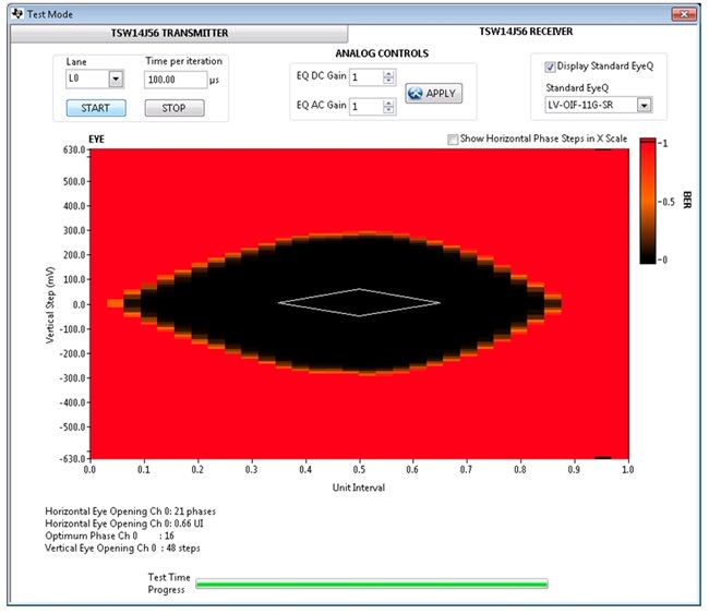
Figure 2 is an example of an open eye diagram acquired using the ADC12J4000 evaluation module (EVM) and TSW14J56EVM along with High Speed Data Converter Pro Software.

Figure 2: ADC12J4000EVM connected to TSW14J56EVM, both using high-performance materials, analog-to-digital converter (ADC) at 4GSPS in decimate-by-4 double-data-rate (DDR) P54 mode (data at 10Gbps) and a default pre-emphasis setting of 4d

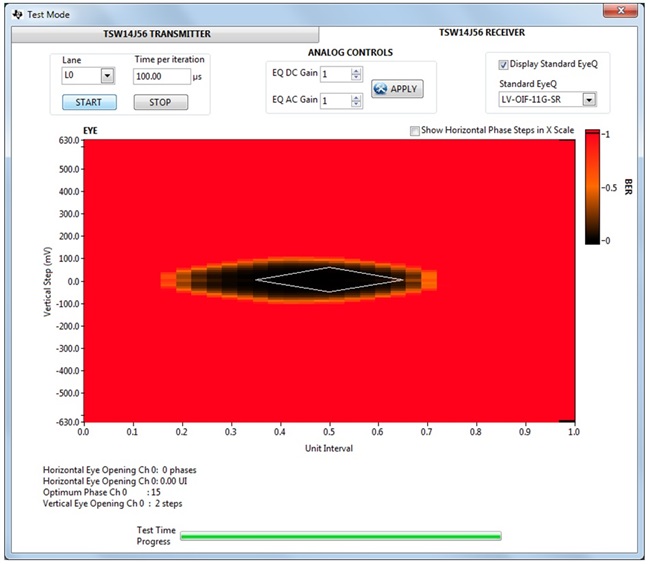
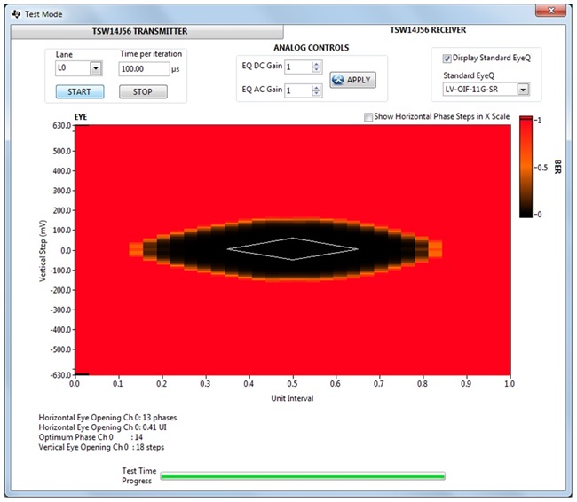
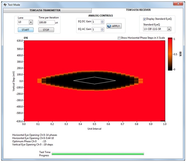
Figures 3 and 4 show the same baseline setup as in the open eye example, but with two different extender boards connected between the baseline EVMs. These extenders were added to evaluate the effects of longer links and lossier materials. Figure 3 is with a 16-inch trace extender board using Rogers RO4350B, another high-performance material. Figure 4 is with a 16-inch extender board using Isola 370HR FR4-type higher-loss material.

Figure 3: Baseline hardware plus 16-inch RO4350B extender board, 4GSPS in decimate-by-4 DDR P54 mode (10Gbps) and default pre-emphasis setting of 4d

Even with high-performance materials, long link distances attenuate the high-frequency signal components and begin to close the signal eye.

Figure 4: Baseline hardware plus 16-inch 370HR extender board, 4GSPS in decimate-by-4 DDR P54 mode (10Gbps) and default pre-emphasis setting of 4d

With a long link using the lower-cost material, the eye quality is severely degraded.

To restore the eye quality at the receiver, you must either select a lower-loss board dielectric or alternatively add some compensation at the serial TX/RX.

Many JESD204B TX/RX devices (ADCs, field-programmable gate arrays [FPGAs]) and digital-to-analog converters [DACs]) incorporate signal-quality compensation circuitry to mitigate the effects of high-frequency signal loss. ADCs will include pre-emphasis (boosting the high-frequency content) or de-emphasis (reducing the low-frequency content) features. On the receive side of the link, DACs and FPGAs may include equalization (adjust gain at different frequencies to optimize the equalizer output eye quality).

Using the TX pre- or de-emphasis feature can allow a system to operate with acceptable receive performance even with lower-cost FR4-type transmission media or longer-than-normal link distances. In these situations, the emphasis features are adjusted until the receive eye meets the specifications with some margin, but without excessive overshoot.

With the same extenders, the ADC12J4000 TX pre-emphasis settings were increased to optimize the data eye at the receiver. Figures 5 and 6 show the eye diagrams after optimizing the pre-emphasis settings for the high performance and FR4 type extenders. A significantly higher pre-emphasis setting is necessary to compensate for the additional loss of the lower-cost material.

Figure 5: Baseline hardware (ADC12J4000EVM + TSW14J56EVM) plus 16-inch RO4350B extender board, 4GSPS in decimate-by-4 DDR P54 mode (10Gbps) and pre-emphasis setting of 7d


Figure 6: Baseline hardware (ADC12J4000EVM + TSW14J56EVM) plus 16-inch 370HR extender board, 4GSPS in decimate-by-4 DDR P54 mode (10Gbps) and pre-emphasis setting of 15d

As I mentioned earlier, the input-signal and clock-signal paths can also drive the requirements of the board materials and stackup. Even if emphasis or equalization features permit link operation using lower-cost board materials, you may still need some higher-frequency layers to minimize signal-quality impacts for the analog or clock signals in a high-frequency design. You must consider all of these factors when selecting the board dielectric materials and planning the board stackup. Once you’ve made those choices you can design, build and test the system. In the testing and debugging phase of the design, you can adjust the TX pre- or de-emphasis settings and RX equalization settings to provide a reliable data link.

Additional resources:

Innovation comes to life inside new ECE facility at the University of Illinois

Four-switch buck-boost controller delivers high power and efficiency

Cool new tools to help boost your analog expertise

$
0
0
Over the years I have sifted through a lot of technical literature, been to many seminars and viewed many online video trainings to gain a better understanding of analog electronics. While there are mountains of excellent material out there, I have noticed...(read more)

Energy harvesting is not new - so why isn’t everybody using it?

$
0
0

Energy harvesting – as most of us know it – has been around for thousands of years. Centuries ago, windmills were used to harvest wind energy. Solar water-heating systems have been in existence since the early 1900s. Since then, people have stretched their imagination to find ways to store and use “free” energy.

Most early energy-harvesting systems were industrial size. Today, the driving force behind the new wave of energy-harvesting devices is the desire to power wireless-sensor networks, or to extend battery life in mobile applications. This led to the development of a technique called microenergy harvesting. A microenergy-harvesting system continuously harvests microwatts to milliwatts of power from ambient sources, storing the energy for later use. Many electronic circuits such as microprocessor-based wireless-sensor nodes require only a few hundred microwatts to function. Thus, a system capable of harvesting small amounts of energy from its environment can practically power a small wireless-sensor node perpetually. Sounds simple, right? But is it too good to be true?

Early barriers to adoption

Large-scale adoption of microenergy-harvesting systems has been slow due to several factors.

First, for a long time, the biggest challenge was the availability of efficient harvester elements (such as solar cells and thermoelectric generators) that gave a higher power output in small form factors. Most harvesters are extremely inefficient converters of energy. For example, only about 20 percent of incident-light energy gets converted to electrical energy in a solar cell.

Second, the high quiescent power consumption of the electronic systems itself was a deal breaker. For example, a system that consumes milliamps of current in its sleep state will create a negative energy balance (more out than in), leading to more reliance on, and eventual depletion of, the system’s battery.

New horizons

These challenges were preventing widespread use of microenergy harvesting. However, now there is serious hope.

With new advances in integrated circuit (IC) ultra-low-power technology, system designers are now able to design systems that consume less power overall, thus making energy-harvesting systems more practical. However, the standby current consumption will still dictate the run time of the battery when harvesting is not possible. In this case, ultra-low standby current will extend the run time of the battery. For example, the TI bq25505 energy-harvester IC has a standby current consumption of 5nA – which is practically nothing. Other industry chips have standby current consumption 300 times more.

The operating-current consumption while harvesting is also critical. Very low operating-current consumption while harvesting means that the majority of the power from the harvester is transferred to the battery. For example, the TI bq25570 has an operating-current consumption of 488nA while other industry ICs have operating currents greater than 5mA – a greater than 10 times increase. Similarly, TI’s ultra-low-power MSP430FR5969 FRAM microcontroller (MCU) has optimized low-power modes that can be creatively used to design ultra-low-power MCU-based systems.

 Harvester providers are taking giant strides in producing harvesters that now give more output for their size. For example, some dye-sensitized solar cells (DSSCs) can now output 20-25µW/cm2 of power at a mere 200Lux (typical office lighting is 600-1,500Lux), thus making microenergy harvesting more attractive. This is more than sufficient to run a small well-designed sensor node whose average power requirement is 60-100µW.

Other requirements

There are other factors that are also critical to the success of an energy-harvesting system.

First is the duty cycle of system – this is decided by the duration that the system is active versus the duration it is sleeping. Total system-power consumption is dominated by sleep current. Hence, by keeping the sleep current as low as possible, extended run times are achievable.

Second, the system should have advanced features such as an maximum power-point tracking (MPPT) feature. The TI bq25570 IC supports MPPT, which is a way to optimize the power extraction from the harvester.

 Third, the system should be capable of intelligently managing the power transfer from the harvester to the battery. Features such as battery management, battery under-voltage and over-voltage protection make the system more robust and safe.

The future

Indoor light harvesting will lead the way to more wide-scale adoption of microenergy harvesting. The applications are potentially huge: home and factory automation, security systems, smart buildings, and medical and fitness applications. TI engineers are ready to assist you in your next innovative design. The question is, are you ready?

Additional resources:

  • TIDA-00041-  Energy Harvesting Reference Design Solution for Ultra Low Power Boost Converter IC
  • TIDA-00242- Solar Power Energy Harvester Reference Design Using Super Cap
  • TIDA-00100- Indoor Light Energy Harvesting Reference Design for Bluetooth Low Energy (BLE) Beacon Subsystem

How to ensure voltage accuracy and processor safety using the TPS65218

$
0
0

As industrial and embedded computing applications become more feature-rich and shrink in size, design specifications in processors and field programmable gate arrays (FPGAs) are becoming more stringent. In particular, voltage tolerance has become much tighter. The new processors have a voltage tolerance of as little as 5% on power rail to ensure safe operation. So it is essential that the converter’s output-voltage accuracy meets the design specification.

Designers can meet design specifications in two ways. They can use a discrete supervisor, but that significantly increases bill of materials (BOM) solution size and cost. Or they can use apower management integrated circuit (PMIC). The PMIC has several advantages.

For instance, the TPS65218 PMIC helps reduce the extra cost of the supervisor significantly and can shrink the total power solution size. It also ensures that the application has high voltage accuracy and meets the processor safety requirements in the specification.


Figure 1: The TPS65218 offers an integrated voltage supervisor with PGOOD signal

The TPS65218 comes with an integrated supervisor monitor with PGOOD signal, four buck converters and a low-dropout regulator (LDO) setup, which means that the PMIC monitors all five supplies of the processors internally. It has two settings: The standard setting only monitors for undervoltage, while the strict setting implements tight tolerances on undervoltage and overvoltage.


In the TPS65218, the PGOOD signal reports the regulation state of the five rails. The output is HiZ when all enabled rails are in regulation and driven low when one or more rails encounter a fault, which brings the output voltage outside the specified tolerance range. A typical application PGOOD drives the reset signal of the system on chip (SoC). Figure 1 shows the behavior of PGOOD on a change in o/p voltage.


You can use I2C to configure the threshold for the accuracy settings and de-glitch time, which gives you the flexibility to adjust the thresholds according to your application needs. The effect of the voltage going out of the specification is that all of the rails of the PMIC are sequenced down. Table 1 shows the various settings for the supervisor configurations. This configurability allows you to scale this power solution to multiple processors and systems.


Table 1: The TPS65218’s supervisor configurations have many flexible settings

Which processor or FPGA could you be powering with the TPS65218?

Additional TPS65218 resources:

The future of data converter interfaces

$
0
0

I’m a very direct individual, and when I think of data-conversion technology, I quickly categorize it into buckets:

  • Precision:  Typically less than 1 Msps with a high dynamic range (+20 bits).
  • General purpose:  Anywhere from 1 Msps to 20 Msps with a moderate dynamic range (12-16 bits).
  • High speed:   20 Msps to 1 Gsps with a good dynamic range (8-14 bits).
  • Ultra-high speed:  1 Gsps and above.

For lower-speed precision and general-purpose data converters, serial peripheral interface (SPI), I2C or parallel interfaces are more than enough to handle the data rate. But what happens when you can now integrate four or eight digital-to-analog converters (DACs) or analog-to-digital converters (ADCs) that each require 100+ Msps per channel? The digital information overwhelms the standard interfaces.

The solution for multiple data converters at or above 100 Msps has been to use either parallel double-data-rate (DDR) low-voltage differential signaling (LVDS) or serialized LVDS. At first, serializing the LVDS seems logical, but LVDS is limited in performance. When serializing large numbers of moderately fast data converters or small numbers (one to two) of ultra-high-speed data converters, lane speeds will exceed 3 Gbps – this is pushing the limits of LVDS technology. In addition, serialized LVDS requires a clock line to synchronize each lane, while the transmission lines still require matching to prevent skew and jitter from affecting bit error rate (BER).

The first true solution to the steady progression of ever-faster analog data converters is the JEDEC standard JESD204. In the latest revision, B, the interface has moved from LVDS to current-mode logic (CML), which is designed for speeds in excess of 10 Gbps. Additionally, the clock is now embedded into the stream, allowing independent clock and data recovery per lane. The standard also introduced scrambling and 8b/10b encoding to both minimize electromagnetic interference (EMI) and improve data integrity. This migration greatly reduces the number of interconnects required between the data converter and processor or field-programmable gate array (FPGA).

For example, an ADC12D1600 running in dual-edge-sampling (DES) mode provides a sample rate of 3.2 Gsps, which requires 50 electrically matched LVDS transmission lines, whereas the ADC12J4000 only requires eight CML transmission lines (which do not need to be electrically matched). The skew is adjusted by an elastic buffer inside the receiver’s JESD204B interface. This also benefits the package, which shrinks from a 292-pin ball-grid array (BGA) (ADC12D1600) package to a 68-pin very thin quad flat no-lead (VQFN) package (ADC12J4000) that is only 10 mm x 10 mm. So both performance and density benefit from this interface technology (Table 1).

Table 1: Comparison of two similar gigasample ADCs, one with a parallel LVDS interface and the other with JESD204B

However, there are issues with this interface technology: latency and signal integrity. One benefit of parallel LVDS is that the delay between the time the sample is acquired from the ADC (or presented to the DAC) is extremely short. In the case of a gigasample ADC, it is a matter of converting a thermometer code to either 2’s compliment or binary – a straightforward digital single-clock cycle function and the data is immediately available at the outputs. In the case of the JESD204B, the data is scrambled, 8b/10b encoded and finally serialized, which all then needs to be reversed at the receiver. This adds considerable latency in the transmission of the data, even with lane speeds of 12.5 Gbps.

Then there’s signal integrity. CML lanes running at 12.5 Gbps on FR4 can be challenging. Beyond the forward-loss factor of the board material, there can be impairments such as connectors and vias that will add to the overall jitter budget of the interface. For longer transmission lines, a buffer/equalizer may be required such as the DS125BR800A, which can provide receive equalization as well as increased drive including de-emphasis to improve the BER of up to eight lanes – a major factor considering that there is no forward-error correction in the JESD204B standard.

So what does the future hold? In much the same fashion that data centers require faster interconnects, so will high-density or ultra-high-speed data converters. The current JEDEC standard specifies CML transmission lines that can run up to 12.5 Gbps. The next-level standard will take that to 16 Gbps or beyond – possibly 25 Gbps – driving the need for careful signal-integrity management and possibly the introduction of more exotic board materials such as Megtron 7. It is the price of going faster, but the benefits of high-speed serialization coupled with standardized protocols outweigh the issues. Till next time …

JESD204B resources:


Maker takes solar energy on-the-go

$
0
0

Maker takes solar energy on-the-go 

We’ve all experienced a power outage in our lifetimes. Wouldn’t it be nice if next time, instead of breaking out the candles and flashlights, you could simply flip on your personal solar-powered generator? Nathaniel VerLee, an electrical engineer and Maker, is developing a solar energy generator to do just that. His generator is an all-in-one application that will not only be able to provide temporary electricity during a power outage, but will also provide power to devices that are not connected to the grid like street lights and mesh networks, as well as provide power to remote areas such as cabins or sail boats.

Nathaniel is currently developing the PCB to go into a “grid in a box” type of application, where a battery, folding solar panel, LED lamps and power cables all fit into a single rugged case for use on camping trips or during power outages. He developed this project as a way to combine his interest in solar energy and desire to use maximum power point tracking (MPPT) in medium-power DC applications.

Nathaniel’s solar energy generator has a buck boost topology DC/DC converter that can step up or step down the output voltage from the input voltage. The generator is based on a Texas Instruments C2000™ Piccolo™ TMS320F28035 microcontroller (MCU), which enables MPPT so that the system can operate at peak efficiency, or the maximum power point. The maximum power point is sensed by TI’s OPA2317 operational amplifiers for current and voltage.  The information is used as inputs to the MPPT algorithm which periodically changes the input to output voltage relationship of the DC-DC converter to determine the MPPT operating point. The system also integrates a TI LMR62014 boost regular IC for 12V rail, a TI TPS54360 buck regular IC for 5V rail, two TI TPS62260 buck regular ICs for 3.3V and 1.8V rail, and gate drivers for the converter. In the final single-PCB solution, a buck converter will be connected to a panel input and the battery, which will source power from the higher of the two voltages. The 5V rail will then supply power for a 12V rail (boost) for the FET gate drivers, and the 3.3V and 1.8V rails will supply power for the microcontroller, sensor circuits, OLED display and other circuits. In addition, a TI ULN2003 high-voltage high-current Darlington transistor array features high-voltage outputs with common-cathode clamp diodes for switching inductive loads. This is critical to protecting the battery from over discharge and short circuit.

Nathaniel chose to use TI’s C2000 Piccolo TMS320F28027 LaunchPad development kit in the prototyping stage of his project since it offers the necessary debugging and programming interface as well as 5V and 3.3V power supplies. He migrated to the C2000 F28035 MCU for development, as this MCU offers the higher pin count needed in his final project as well as many peripheral features ideal for digital power applications. “Configuring [the F28035 MCU] to drive the buck boost converter is not only easy, but powerful, allowing multiple converters to be driven in a phase relationship, and for fast shut down of the converter stage in the event of a dangerous transient event,” said Nathaniel. As a self-proclaimed analog and power engineer, Nathaniel also appreciated the simplicity and low cost of entry of using the Code Composer Studio™ integrated development environment with the XDS100 debugging tool to tackle this embedded project.

Nathaniel also commented on why he chose TI’s boost and buck regular ICs, which are abundant in his project. “I like that TI has a comprehensive portfolio of ICs for generating rail voltages,” he said. He also enjoys being able to use TI’s WEBENCH® design environments to quickly develop designs with less time and effort.

This solar energy generator is a side project that Nathaniel works on in addition to a full-time job, and his biggest obstacle has been finding time to stay on track and design his project on weekends. He says that although he may eventually decide to sell the hardware as a complete product, his main objective for now is using the project as “more of a learning and exploration platform that [he] hopes to eventually share with others in some sort of hobby or educational type capacity.” He also hopes to experiment with different features and test them in the hands of other engineers to see which features will be most useful in his generator.

Although this project has been quite an undertaking, Nathaniel says, “Living during a period of rapid growth in energy saving technologies is very exciting to me – I hope that as these technologies grow, they help save energy and work towards reducing our environmental footprint.”

Learn more about Nathaniel’s progress on this project on hackaday or his personal website, and let us know in the comments – what solar applications do you see being most useful in the future?

Our BIGGEST launch yet – Introducing the new MSP43…

$
0
0

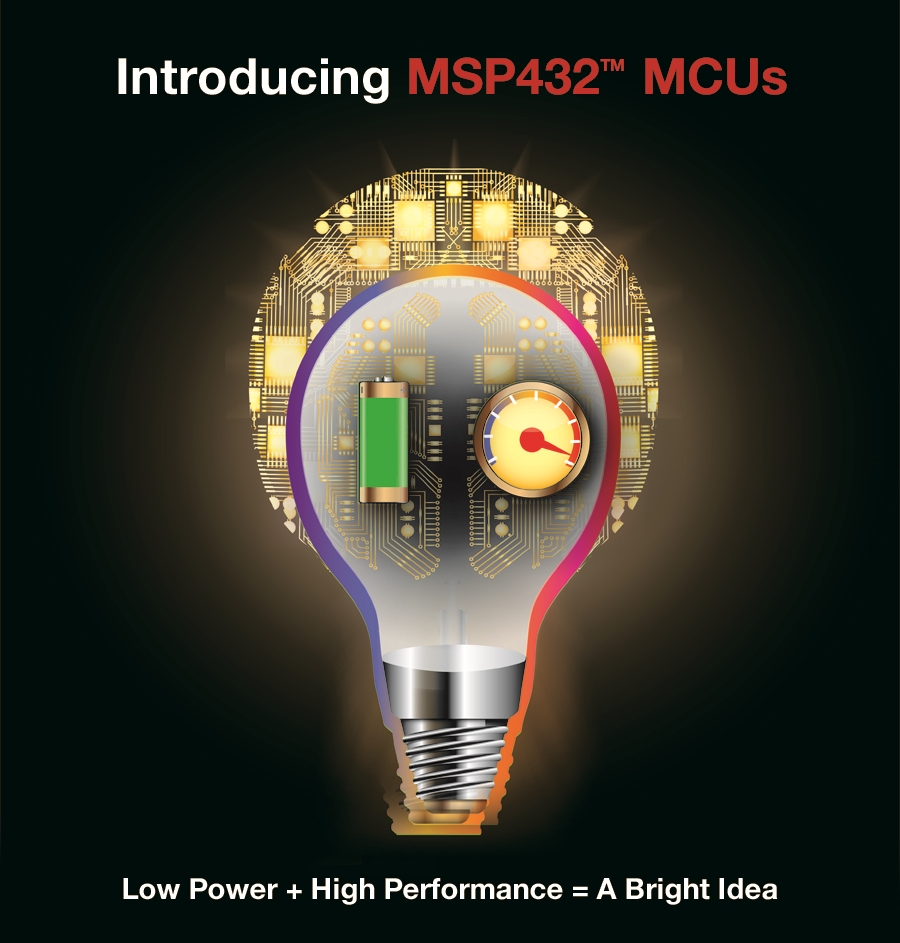
 Today we unveiled the brand new ultra-low-power MSP...4...3...2 microcontroller platform! Yep - MSP432 MCUs!

Any guesses yet what that means? Did you guess 32-bits? An ARM® Cortex® core perhaps? Correct and Correct! We hope you’re excited to learn TI is bringing its low-power MSP430 DNA to the ARM world! Imagine an ARM Cortex-M4F core, now combined with the low-power benefits you've come to expect with MSP430 MCUs. With an FPU engine, DSP instructions and 48MHz -- MSP users looking for more performance or an industry-standard core, or ARM users looking for lower power, will find the best of both worlds. Our 16-bit MSP430 MCUs will continue to be the foundation of our portfolio and we will continue to bring you new innovations in the 16-bit space, like our MSP430 FRAM family.

You may be surprised to hear that you can now get all the performance of a Cortex-M4F, but with similar power as a Cortex-M0+! No more compromises or balancing tradeoffs of low power and high performance in your industrial or consumer applications. Our MSP432 MCU platform is officially the industry’s lowest power ARM Cortex-M4F device out there. A lot of companies claim "low-power MCUs", but we now have a way to prove it – check out EEMBC’s ULPBench that provides an apples-to-apples comparison of power consumption across MCUs. MSP432 MCUs have the highest score (167.4) among competitive Cortex-M3 and -M4F devices - and in case you're curious - the higher the score, the lower the power!

TI designed the MSP432 MCU platform to be the industry’s lowest power ARM Cortex-M4F device to consume only 95uA/MHz in active, 850nA in standby with RTC and included peripherals optimized for ultra-low power, such as:

  • An integrated DC/DC (in addition to an LDO) that saves 40% more power vs. an LDO
  • 64KB of RAM with selectable retention on eight independent banks that saves 30nA per RAM bank
  • Low-power high speed ADC consumes only 375uA when sampling sensors at 1MSPS
  • Driver Library stored in ROM consumes 35% less power than Flash

At the same time, TI packed in new high performance peripherals around the core that enabled us to get the highest CoreMark score possible of 3.41/MHz. This includes features like:

  • 256KB of Flash with independent banks, that let you simultaneously read and erase from flash
  • Driver Library stored in ROM that enables you to execute 200% faster vs. Flash
  • Sample from sensors faster with MSP’s fastest ADC yet – a 1MSPS 14-bit SAR ADC with 13.2 ENOB

 Of course, we're not just announcing the silicon - we've got the MSP432 LaunchPad available to order for only $12.99! You don't have to adjust your eyes, yes - it’s black! 

TI has released a limited-edition MSP432 LaunchPad on black PCB to commemorate the fifth anniversary of its LaunchPad development ecosystem. For a limited time, you - our dedicated community of first adopters can pick up a black MSP432 LaunchPad through the TI Store and authorized distributors for $12.99 MSRP. (Once supplies are depleted, a traditional red version will be sold in its place at the same price).

After you take a look at the out-of-box demo– get started programming your own application using MSPWare that contains over 150 code examples, along with training, app notes, user’s guides, and DriverLib.

So get started today adding more performance to your application, while reducing your power with the MSP432 LaunchPad. If you want to learn more about this innovative new platform, check out our new white paper

DIY with TI: Inventing the perfect game show buzzer

$
0
0
At TI, we celebrate the makers and hobbyists who enjoy creating and innovating on their own time. In our ongoing DIY with TI series, we share their incredible Do It Yourself inventions using TI technology. The buzzer is as synonymous with game shows...(read more)

Doing the math: The inside story of the Analog Engineer’s Pocket Reference

$
0
0

As an analog applications engineer, much of my problem-solving involves recommending application circuits for customers to use as subcircuits in their overall product design. Thus, I understand the need for standard values, formulas, printed circuit board (PCB) characteristics and shortcuts for predicting performance.

A colleague of mine, Tim Green, has about 32 years of experience, of which 16 are in board-/system-level design. When I asked him how he handled these common design aids, he opened his file cabinet and pulled out a folder stuffed full of dog-eared and well-worn papers he’d collected over the years of his favorite design collateral. One of the things that fell out was a small 25-page booklet called “The Burr-Brown Electronic Engineers Pocket Reference,” published in 1994.

That booklet was the motivation for Tim and I to modernize, simplify, organize and electronically publicize the new Texas Instruments Analog Engineer’s Pocket Reference (Figure 1).

Figure 1: TI’s new Analog Engineer’s Pocket Reference inspired by a 1994 Burr-Brown booklet

One general problem with pocket references is that you have to be really familiar with them. In other words, when confronted with a difficult problem, you might resort to a Web search before using the pocket reference if you don’t know that the answer is in the pocket reference.

So in order to help familiarize you with the new TI pocket reference, I have put together some questions. Try to answer the questions using the pocket reference and you will gain a much deeper understanding of the book’s powerful content.

Question 1 (hint: Analog section):

Referring to the circuit below, what is the phase shift at 100kHz?

Question 2 (hint: Amplifier section):

Referring to the circuit below, what is the rise time for the 20mVpp step wave input? Note that this is a small signal step and the OPA209 has a gain bandwidth product (GBW) of 18MHz (data sheet SBOS426).

Question 3 (hint: Amplifier section):

What is the noise spectral density of a 10kΩ resistor?

Question 4 (hint: Amplifier section):

Given the transient closed-loop waveform shown below, what is the loop gain phase margin?

Question 5 (hint: PCB and Wire section):

Referring to the figure below, what type of package is this?

Question 6 (hint: Sensor section):

What is the resistance for a PT100 resistance temperature detectors (RTD) at 100℃? Assume that the RTD adheres to the ITS-90 standard.

Question 7 (hint: A/D Converter section):

Calculate the effective number of bits (ENOB) for an analog-to-digital (A/D) converter assuming signal-to-noise and distortion (SINAD) (dB) of 75dB.

For the benefit of those who are still working through the problems, please do not post answers in the comments. I will post the answers next week. Good luck! 

Additional resources:

Download the Analog Engineer’s Pocket Reference to get often-used A/D conversion formulas in one place.  

VIDEO: Why we believe diversity fuels innovation

$
0
0

Why are we passionate about educating and engaging the next generation of engineers? From first time learners in kindergarten to students pursuing higher education - finding creative solutions to problems requires a team of minds with different perspectives and life experiences. This is the best environment to fuel creative and innovative thinking which is a critical ingredient for solving the challenges of tomorrow.

Watch the below video to see why we believe diversity fuels innovation and why it is so important to us. 

(Please visit the site to view this video)

Read our full blog post to learn more about this video. 

Learn more about how we support diversity fueling innovation. 

Viewing all 4543 articles
Browse latest View live


<script src="https://jsc.adskeeper.com/r/s/rssing.com.1596347.js" async> </script>