Since its definition in 1983, RS-485 has become the preferred interface standard for many industrial fieldbus applications. In this RS-485 basics series on the new TI E2E Community Industrial Strength Blog, we hope to create present a useful, informative...(read more)![]()
↧
RS-485 basics: Introduction
↧
Power Tips: Synchronize your SEPIC
A single-ended primary-inductor converter (SEPIC) does a great job of bucking or boosting the input voltage to maintain a regulated output voltage. This is useful in automotive applications or systems that may have multiple input sources available, but you don’t necessarily want to change the converter type. A SEPIC has many advantages, such as minimal active parts, and requires only a low-cost boost or flyback controller. However, like all topologies, it can also come up short in certain performance areas. One of these shortfalls is a limited maximum output current due to diode rectification. Let’s take a look at how synchronizing the output can help.
Figure 1 shows a basic SEPIC circuit, while figure 2 details the corresponding key voltage and current waveforms. When Q2 turns on, it conducts the sum of the currents flowing in each winding of L1. This sum is equal to the input current plus Iout and reaches its maximum at full load and minimum input voltage. When Q2 turns off, these two currents are diverted through D1, into the output capacitor and load. Current only flows in D1 after Q2 is off because D1 is reversed-biased when Q2 is on.

Figure 1: A coupled-inductor SEPIC converter has two current paths

Figure 2: Key waveforms for a continuous-conduction-mode (CCM) SEPIC
The magnitude of the current flowing in D1 is Iout/(1-D), as shown in Figure 2. The conduction current may be significantly larger than Iout for input voltages much less than Vout, where the duty cycle becomes large. It’s easy to see that when operating at 50% duty cycle, where the input and output voltages are equal, the current in D1 is twice the output current. The average current in D1 is Iout, but to calculate the power dissipation in D1, it’s necessary to use the diode’s forward-voltage drop at the higher Iout/(1-D). This makes the maximum diode dissipation calculable by equation 1:
 (1)
(1)
Calculating the power dissipation with Iout/(1-D) may require the use of a diode with a higher current rating than anticipated, as well as a thermally enhanced package.
Figure 3 implements a synchronous SEPIC converter with an LM5122 sync-boost controller. It allows the use of an N-channel metal-oxide semiconductor field-effect transistor (MOSFET) (Q1) to replace diode D1, thereby reducing losses or allowing more output current for the same losses.

Figure 3: A sync-SEPIC converter implemented with a sync-boost controller and floating-gate drive improves efficiency
A SEPIC has two switching nodes (TP2, TP3) rather than the single switching node of a boost. The gate of the SEPIC’s sync FET (Q1) cannot be directly connected to the boost controller’s high-side driver because its source (TP3) is not at the same potential as its SW pin (TP2). To drive it, I added a floating level-shifter circuit comprising R3/D2/C15. C15 has a voltage drop of VIN across it, which is the same voltage as the “flying” capacitor C1, providing the correct voltage swing across Q1 gate-to-source. R3/D2 restores the proper gate-drive offset (low = -0.5V, high = 7V).
To summarize, the rectifier losses in a SEPIC converter can impose a practical limit on the desired maximum output current because of thermal limitations. As the converter’s input voltage decreases, the diode’s conduction current increases, increasing losses, raising temperature, and hurting efficiency. By replacing the diode with a synchronous FET, it’s possible to reduce these losses. In the example circuit shown in Figure 3, the output current is increased by more than 1A over a traditional SEPIC with the same losses. Synchronous rectification obtains an efficiency greater than 95%.
For more about this topic, see this Power Tips article: “Three Ways to Boost Performance of a SEPIC.”
Additional resources
- TI Designs reference PMP10886 REVA, “12V@5A Synchronous SEPIC Converter Reference Design.”
- Check out TI’s Power Tips blog series on Power House.
↧
↧
Why Trade Promotion Authority matters for Sherman, Texas
 This editorial from Heidi Means, manager of our Sherman Wafer Fabrication Facility, first appeared in the Herald Democrat on April 21, 2015.
Texas is No. 1 — for the 13th straight year. Recent U.S. Commerce Department figures released for 2014 show the Lone Star State led the nation with goods exports worth $289 billion, up 3.4 percent from 2013, and representing 17.8 percent of all U.S. goods exported. International trade is vital to Texas, directly supporting 3 million jobs. Trade-related jobs grew 1.6 times faster than other employment in the state, and now represent one in every five jobs, according to the Trade Benefits America Coalition. A new bill in Congress would help expand and open markets for Texas products and services to reach the 95 percent of the world’s consumers outside the United States.
Last week, bipartisan members of Congress introduced legislation to reauthorize Trade Promotion Authority (TPA). Under TPA, Congress sets clear goals for U.S. negotiators to secure the best market openings for U.S. companies and workers and resulting trade agreements are then allowed to be considered with a simple up-or-down vote from Congress. Since Franklin Roosevelt, presidents have had this authority.
Here in Sherman, Texas Instruments manufactures chips used in electronic products that are sold all over the world. But the road from Sherman to the end customers is complex. Increasingly global supply chains support the competitiveness of U.S. manufacturers like TI. For example, a typical TI chip made in Texas will travel the world before it appears in your car’s electronics, digital camera, smartphone, gaming system or medical device. After being made in our factory in Sherman, the chip could be sent to Malaysia, Philippines or Mexico to be assembled, tested and packaged. It could then get sent to our product distribution center in Singapore before being shipped to TI Korea where it could be sold to a Korean electronics manufacturer who might then sell it to any number of countries. In short, a chip small enough to fit on your finger that could sell for less than a dollar could travel literally around the world before it gets to the end user.
Read the full editorial from Heidi in the Herald Democrat.
↧
Understanding Voltage References, Part 1 - Shunt versus series: Which topology is right for you?
There are two types of voltage references, shunt references and series references. Each type has its own usage conditions and the process of selecting between the two can be intimidating. Comparison tables do exist, but they typically provide little insight on how to choose one reference topology over the other for specific applications. This blog series will discuss the applications of both shunt and series references and when to use them, as well as highlight some lesser known use cases for each reference topology.
Part 1 - Shunt versus series: Which topology is right for you?
The real world is analog (for now at least), and the most common way to interface with the real world is to use analog-to-digital converters (ADCs), sensors or other application-specific integrated circuits (ICs). A voltage-reference IC provides a stable output voltage that can be used as a constant value as system voltage and temperature change. There are two types of voltage references – shunt and series– and each has its own set of strengths and use cases, listed in Table 1.

Table 1: Typical comparison table of shunt versus series voltage references
A shunt reference is functionally similar to a Zener diode, where the voltage drop across the device is constant after the device reaches a minimum operating current. The shunt reference regulates the load by acting as a constant voltage drop and shunting excess current not required by the load through the device to ground. There is no maximum input voltage rating for a shunt reference, but an external resistor , is required. The input supply will always see the maximum load current as determined by the input voltage level and the external resistor. The shunt reference will sink more or less current as the current requirements of the load change.
The external resistor must be between and , as calculated by Equations 1 and 2:


You can also use a shunt reference to create floating references and negative references, and the equations for calculating remain the same.
A series reference device does not require an external resistor, and only consumes as much current as required by the load plus a small quiescent current. However, the input voltage is passed directly into the reference device; therefore a series reference does have a maximum-rated input voltage. The series reference may include an enable pin to externally enable or disable the device to save power.
When selecting a voltage reference for your next application, be sure to keep the typical use cases below in mind.
Shunt reference use cases:
- Wide-input voltage range or high-input voltage transients.
- Negative or floating voltage references.
Series reference use cases:
- Variation in load current, where a series will see lower for lighter loads.
- Reference with sleep or shutdown operations.
In part two of “Understanding Voltage References,” I will discuss ultra-low dropout and how it is not just for the series reference.
In the meantime, visit www.ti.com/vref for more information on TI’s voltage reference products and for a detailed explanation of voltage-reference selection with respect to ADC resolution, download the white paper “Voltage Reference Selection Basics.”
↧
How to Power the Internet of Things

Have you been looking forward to a world where everything is smart and connected? A world where millions of sensor networks are deployed throughout homes, offices and factories to help make better decisions, keep people safer, enable more automation, reduce cost, and improve everyone’s overall productivity and quality of life? If your answer is yes, the good news is that this world, called the Internet of things (IoT), is just around the corner.
So what is IoT? It’s the concept that everything – literally every single “thing” on Earth (and even beyond) – will be assigned a unique address. This address allows each and every thing to communicate and interact via the Internet with every other thing.
Currently, a “thing” is defined as a device with the capability to connect to the Internet. That includes cellphones, smart TVs, refrigerators, coffee makers, jet engines, nuclear reactors, and anything else with an on and off switch. But the concept is much bigger than that. As communications technology (particularly wireless technology) becomes more advanced, there is little that will keep everything from becoming “smart.” Of course, TVs, refrigerators and coffee makers have been around for years, but only recently have they been able to connect to the Internet. Could you imagine how many other things could become connected as technology advances?
As shown in Figure 1, the number of connected objects as of February 2015 is around 14.8 billion, but will reach around 50 billion by 2020.

Figure 1: IoT Growth Forecast (image courtesy ZDNet.com)
IoT, emerging as technology’s next megatrend, is opening up a host of new opportunities and challenges for the semiconductor industry. How to power these devices has become a question for every solution designer. Energy harvesting and wireless power technologies can help enable small batteries or battery-less solutions and eliminate power cords.
With billions of sensor nodes, the time it takes (and cost) to replace batteries is substantial. Many wireless sensors will need to be self-powered. Harvesting energy from the ambient environment becomes a favorable solution, either by extending time between battery changes by topping up rechargeable storage devices or eliminating them all together. There is a wide range of energy sources available, including solar, thermal, vibrational and even ambient radio frequency (RF). TI power-management devices can work with a wide range of harvester, storage and load technologies to extract the maximum amount of energy from various sources.
The IoT has also been driving new semiconductor investment in low-power electronics like wearables. Wearable devices, or “wearables,” have started to revolutionize personal fitness. The inconvenience of different charger cables and connectors for these tiny devices is an increasing inconvenience for consumers. Wireless power can remove this burden and improve the overall user experience, making it a catalyst for adoption. Credit Suisse predicts that smartphones will become the “personal cloud” for wearables, and the average customer will have at least one if not two of these products close by at all times within five years. Technology research firms predict that the wearable wireless device market will grow to $6 billion by 2016.
The five TI designs below provide reference circuitry to enable customers to introduce very small and efficient wireless-power, battery-charging and energy-harvesting solutions to their applications. Check them out. It’s time to power your IoT device!
- TI receiver design: Qi (WPC) Compliant Wireless Charger for Low-Power Wearable Applications.
- TI receiver design: Tiny Wireless Receiver for Low-Power Wearable Applications Reference Design.
- TI transmitter design: Small Wireless Power Transmitter for Low-Power Wearable Applications.
- TI transmitter design: Low-Power Wearable TX Reference Design.
- Sensor node for IoT design: PMP9754
↧
↧
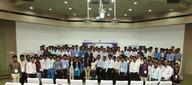
India Design Contest Semi-Finals: Last Leg of the TIIC 2015 Train Journey (Part - II)
After traveling to Mumbai and Delhi, the 2015 Texas Instruments Innovation Challenge (TIIC) India Design Contest train reached the next semi-finals stops – Bangalore and Chennai.
The Bangalore Semi-Final

Teams from 25 engineering colleges located in Karnataka, Andhra Pradesh participated in the semi-finals held at the Indian Institute of Science Bangalore.
To address the increasing number of traffic jams in metropolitan cities, students from Manipal Institute of Technology engineered a smart traffic light powered by harvested solar energy that controls the switching of traffic signals based on the traffic density. A team from RV College of Engineering demonstrated an automated cooking machine which can cook a variety of pre-programmed Indian dishes. This machine also automates vegetable cutting and stirring while cooking.
Click here for the projects demonstrated at the Bangalore semi-final
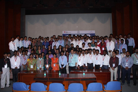
The Chennai Semi-final
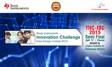
The Chennai semi-final which was hosted at Indian Institute of Technology, Madras featured 22 teams from Tamil Nadu, Kerala and Sri Lanka.
Driven by the goal to provide a safer environment to workers in the wood industry, students from SRM University built a low-cost electromechanical setup which incorporates a Passive Infrared (PIR) sensor to detect human proximity. The mechanical setup is designed as to pull down the moving blade in event of any worker coming closer to the blade and thus prevent an accident.
Click here for the projects demonstrated at the Chennai semi-final.
Praise for the Students
At all semi-final events, students’ commitment, insight, and diligence impressed all who were present. Representatives from TI Customer Companies like HCL Technologies, Tata Consultancy Services, Tech Mahindra, Swelect Energy Systems Limited, Melange Systems Private Limited and Elmeasure were in attendance, a few seeking recruits from the participating teams.
Professor Dhananjay Gadre of NSIT Delhi who has been associated with TIIC as a faculty mentor from last 3 years, observed an improvement in the quality and completeness of the projects in the TIIC 2015 semi-finals, when compared to the finals of previous years.
Several of the projects not only supported social causes, but also have commercial potential. Mr. Uday Wankawala, a consultant from NEN Global commended the close involvement of the faculty in guiding and mentoring the students and urged exploration of the possibility of an industry mentor for each participating team.
Student Speak
Students, through the process of developing their projects, acquired key attributes for working in Industry like a deeper understanding of technology concepts, collaborative skills of working in a team and delivering within strict timelines. Compared to other national-level contests, students observed that TIIC focused more on innovation and TI offered a much wider range of components to use in their projects. In addition, TI provided—as the teams termed it—the “best support” in the form of online documentation and through the TI E2E Community forum.
The Last Honk!
The TIIC train is ready for the last leg of the journey. Our reviewers have selected 14 teams for the TIIC 2015 finals who will compete for the Chairman’s Award. The shortlisted teams will now have to step up their preparations and convert their prototype into a well-defined product which will be demonstrated in the TIIC Finals. We thank all the teams for participating in TIIC 2015 and hope that it was a good learning experience. We encourage you to stay connected with TI India University Program by registering on my.ti.com and by joining us on Facebook!
↧
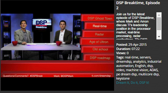
This Town is Coming Like a Ghost Town - DSP Breaktime: Episode 2
It’s time for Episode 2 of DSP Breaktime and it’s out just in time before everyone's attention turns to Age of Ultron. In this video you’ll find:
Main topics:
- DSP Ghost Town – discussion of the state of DSPs in the market
- Real-time processing – what it is,why it’s important and what it means for design
- Radar – great application for DSPs (read our SAR white paper)
Wrap-up
- Age of Ultron – because we had to
- Old school – early computer memories
- DSP roadmap – a serious diversion in the normally light wrap-up section
- Hearthstone – if you don’t know, don’t ask…
You can watch the video here.
As always, Mark and I would love your comments and feedback as we continue with this series in our attempt to provide our views on the DSP and Embedded processing world. And don’t forget to bookmark the DreamDSP page and check periodically for future videos and collateral in our Dream DSP campaign.
And to anyone who gets the title, you most likely have an old school computer memory to share...
↧
Seventh grader imagines way to reduce energy consumption
 TI engineers gather around Annalisa Minke as she calmly, yet passionately, explains how her innovation will cool homes and businesses without contributing to global warming. Her ingenious concept involves engineering air traps to bring cooler air from the top of a structure to the bottom, improving air conditioning systems. Annalisa isn’t a TI customer or a graduate student from a leading engineering university – she’s a seventh grader from a middle school in Tucson, Arizona.
“My house has a swamp cooler, and I hate it because it smells like fish,” 12-year-old Annalisa said with a smile. “I was wondering how people kept cool before they had electricity. I found that in ancient China and Babylon they used cooling towers, and I wanted to know if one could be used in today's houses. I built a model of a house with a cooling tower, and it did keep the house cooler.”
Annalisa was just one of more than 5,000 students from grades K-12 who recently participated in the TI-sponsored Southern Arizona Research, Science and Engineering Foundation competition. It’s one, gigantic science fair with a more than 60-year history of students in the southern half of the state showcasing their best ideas. And for the last seven years, TIers have contributed their expertise and know-how to helping students and teachers succeed in the annual competition.
 “Our involvement is so much more than just a week in March every year,” said Jake Klein, an analytical development manager for device analysis services at our TI Tucson site. “We help teachers across Arizona understand what the fair is and how to assemble a project, grasp the scientific method and give engineering, science and math guidance.”
During the week of the fair, TIers act as judges, handing out first, second and third prizes to the best middle and high school projects. Edwin Collier Moody V received TI’s top high school prize for, “mathematically modeling the performance of biofuel in a diesel engine as an alternative to the standard gasoline engine in a widely used Unmanned Aerial Vehicle.” Annalisa’s project won the top TI prize for the middle school division.
“My favorite part of competing was the spoils of victory. I feel the prize at the end of all our work is very beneficial. It helps me feel the importance of working hard for a reward,” Annalisa said.
Jake said this science fair does so many things to encourage and excite more students interested in science, technology, engineering and math. For example, the competition extends beyond the high- and middle-school levels, attracting students as young as six years old.
“We found that students at an earlier age could get turned off by science or don’t get to see the excitement of STEM studies in their everyday curriculum. With this science fair, they see the fun side of STEM, and very well could direct their future as they progress through school.”
 Another example: This year, 57 percent of the participants were girls, a group typically underrepresented in STEM fields.
“Many times, girls think STEM is more of a man’s field or not a cool thing to do,” Jake said. “Through this event, there is a lot of focus on encouraging underrepresented minorities and females to participate and learn the value of a possible career as a scientist or engineer.”
And for the middle school winner, Annalisa, she’s thinks the competition and STEM subjects are just as cool as her award-winning project.
“I entered into the science fair due to the fact that the whole competitive process is very good practice for the real world,” she said. “Learning how to work hard is an excellent life skill because to be successful as an employee you need to work hard. Competing will help me in college and when I look for a job.”
↧
Understanding Voltage References, Part 2 - Ultra-low dropout: Not just for the series reference
Have you ever needed a voltage reference that has to tolerate wide-input voltage ranges yet is still capable of low-dropout operation? For example, most series references with low dropout do not support up to 12V. This is where a shunt reference can be very handy.

Figure 1: Driving an ADC external-reference pin with a shunt reference
In the application shown in Figure 1, the LM4040 shunt reference voltage is 4.096V, which is a common choice for analog to digital converters (ADCs) because 1 mV is equivalent to one least significant bit (LSB) with a 12-bit ADC.
The shunt reference requires an external resistor to set the supply current. The load current for the voltage reference can be determined from the ADC data sheet. For this example, let’s use the ADS8320. In the circuit shown in Figure 1, the current draw of the external reference pin is listed as 40µA in the ADC data sheet. With an external resistor value of 576Ω, the voltage reference will remain in its operational area over an input-voltage range of 4.16V to 12.75V. That’s a dropout voltage of 64mV, with full reference functionality beyond 12V. To compare the shunt reference low dropout to a series reference with the same 4.096V reference voltage, the dropout voltage for the REF5040 should be listed as 200mV in the data sheet.
If 64mV isn’t low enough for you, using an external resistor value of 100Ω allows for an even lower minimum input voltage of 4.11V and a dropout of 14mV. The trade-off of this ultra-low dropout is illustrated by the maximum input voltage, which would be limited to 5.59V before the quiescent current exceeds the device’s maximum rating. To compare this to a series reference again, the REF3240 has a low dropout of 5mV but a maximum input voltage of 5.5V. Note that the series dropout improvement is with a different part, while the shunt is the same part with a different resistor.
Table 1 summarizes the voltage and current values for the two resistor values for the LM4040 shunt reference.
RS | ILOAD | VINMIN | IQ at VINMIN | VINMAX | IQ at VINMAX |
576 Ω | 40 μA | 4.16 V | 71.1 μA | 12.75 V | 14.98 mA |
100 Ω | 40 μA | 4.11 V | 100 μA | 5.59 V | 14.9 mA |
Table 1: Voltage and current parameters for different external resistors of the LM4040 shunt reference
These very low dropout voltages are possible because the load current seen by the reference device is very small at 40µA. If the load were 100µA, the same 576Ω resistor would allow for a minimum VIN of 4.2V with a dropout of 104mV, which is still low. In applications with higher load currents, the dropout will increase as the required resistance increases.
In part three of “Understanding Voltage References,” Liz Marek will explain how to achieve shunt reference flexibility with series reference precision.
In the meantime, visit www.ti.com/vref for more information on TI’s voltage reference products and consider these additional resources that can help you with your design:
- Part 1 of this series discusses the differences between a series and shunt voltage reference “Shunt versus series: Which voltage reference topology is right for you?”
- For a detailed explanation of voltage-reference selection with respect to ADC resolution, download the white paper “Voltage Reference Selection Basics."
↧
↧
CAN we start at the very beginning?
Welcome to the first post in a new series about the controller area network (CAN). Our intention with this series is to provide a well-thought-out overview of CAN, starting with the basics, and quickly get into feature details and common application questions...(read more)![]()
↧
Using Hall effect sensors in your rotary encoder application
Rotational sensing is used in a variety of applications, including cars, motor shafts and turbines. Traditionally in these types of applications, designers have used mechanical or optical solutions to sense rotation, but with drawbacks.
Learn how you can use a Hall sensor to measure speed or two to measure speed and direction magnetically in your rotary encoder application. Contact-less Hall effect technology senses a magnet that is built into the knob and allows designers to do the same type of quadrature output (signals that are 90 degrees out of phase) that traditional rotary encoders use but with higher reliability and accuracy, while reducing bill-of-materials and system cost.
Read more on the Behind the Wheel blog.

↧
From crops to store shelves, the future is looking bright for near-infrared spectroscopy
While they’ve existed for 60 years, few realize the importance of near-infrared (NIR) spectrometers for measuring energy reflected from or through various materials.
NIR spectrometers help an array of industries -- agriculture, forensics, pharmaceuticals...(read more)![]()
↧
How are washing machines like bats? Using sound to improve our lives.
Austin, Texas has many attractions — music, technology and food, to name a few. But for visitors in the summer months, there is one attraction that no one should miss. Every day at dusk, up to 3 million bats fly out from under one of the city bridges...(read more)![]()
↧
↧
FPGAs & PMICs: Perfect companions for next generation Industrial systems
Most modern field programmable gate arrays (FPGAs) are integrated with ARM cores in order to offer the performance and power savings of application-specific integrated circuits (ASICs) and the flexibility of programmable logic. An FPGA’s flexibility usually provides bliss for industrial programmable logic controller (PLC) or motor-drive designers but woe for power designers.
One of the biggest challenges power designers face when designing power solutions for these systems is how to keep the number of components to a minimum on the board, how to design a power solution for the system that is as flexibility as an FPGA, and how to accommodate various FPGAs and future power needs. It is very important for designers to keep these three factors in mind to reduce the design cycle and speed time to market.
In a recently released TI Designs reference design, we show how to power the Zynq 7015 FPGA with the TPS65911 power management integrated circuit (PMIC) on less than 2 square inches of board area. The distinctiveness of this power solution is that it cannot only power the Zynq 7015 with 5W of application, but it can effectively power 8W and even 16W applications. It’s not just appropriate for different levels of power; the solution is capable of powering the Zynq 7020 and 7030 FPGA families as well.
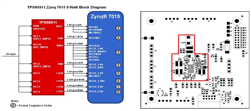
Figure 1: Solution for Zynq 7015 using TPS65911
You must be wondering what is so different about the PMIC. Its main feature is that it contains the perfect combination of three DC/DC converters and one DC/DC controller. The DC/DC controller allows the design to scale the load current required by the system and usually powers the core of any processor or FPGA.
The power field-effect transistors (FETs) of the controller are not integrated into the PMIC, which allows you to select the right FETs for your system power needs; the FETs can vary in RDSON based on the power requirements. Plus, the DC/DC power rails are dynamic voltage frequency scaling (DVFS)-capable, which saves power during low-power operation.
Another important feature that makes this device capable of powering multiple generations of FPGAs is the fully programmable integrated sequence, which can be changed with the help of boot pins on the device and the electrically erasable programmable read-only memory (EEPROM) memory in the device. The boot pins can select two flashed power sequences.
Given these options and flexibility, which FPGA could you power with the TPS65911?
If you're looking for other advice, check out this blog on increasing voltage tolerance and accuracy in FPGAs.
↧
Simple solutions for supplying your isolated delta-sigma modulator
The AMC1304 reinforced isolated modulator family is designed specifically for systems, such as motor controllers and solar power inverters, where the presence of high voltage demands the use of an isolation barrier in order to protect both the end user and sensitive components. Because of this isolation barrier requirement, you’ll need two power supplies: one for the analog input side (also referred to as the high side) and another for the digital interface side (also referred to as the controller side).
On the controller side, many isolated acquisition systems have a 3.3-V DC supply; on the other side of the isolation barrier, however, there may not be a suitable power supply for the AMC1304. Thankfully, there are some ways to get around this.
Zener diodes provide the simplest solution in a system where a DC-floating power supply is available. Figure 1 shows an example of this approach.

Figure 1: Zener-diode-based high-side power supply
You can achieve a more energy-efficient solution in multichannel systems by using the same approach described in this article. That approach consists of a step-down switching regulator (Figure 2) followed by multiple copies of push-pull drivers (Figure 3).

Figure 2: Step-down switching regulator

Figure 3: Isolated supply from 3.3V DC
If the system uses only one sensing channel, then you can use the power supply shown in Figure 4.

Figure 4: Efficient power supply option for a single-channel system
You can obtain and modify the power-supply solutions shown in Figures 2, 3 and 4 through TI’s WEBENCH® design and simulation tools.
To monitor variables in AC power lines, capacitive-drop (cap-drop) power supplies are typically less expensive than their switching-mode counterparts. Figure 5 shows a cap-drop supply for the AMC1304 family.
Figure 5: Cap-drop supply for AMC1304 family
Designing this type of supply is relatively straightforward. Choose the value of C1 from the load current (in this case the maximum AVDD supply current to the LDO_IN pin of the AMC1304 family), the peak line voltage (assuming that the line voltage is sinusoidal at 120VRMS) and the line voltage frequency (60Hz), as shown in Equation 1:
Equation 2 shows how to calculate the value of the capacitor connected to the low-dropout (LDO) input of the AMC1304 family for a given maximum LDO input ripple (ΔVMax). In Figure 5, this capacitance is obtained through the parallel combination of C2 and C3.
In Figure 5, Z1 is a 12-V Zener diode that establishes the maximum LDO input voltage (for example, the BZT52C12S Zener diode can be used for Z1). In Figure 5, D2 can be a Schottky diode with low forward voltage and more than 20V of reverse breakdown voltage (for example, the DB2J31000L and CDBU0230 Schottky diodes can be used for D2). In Figure 5, R4 is included for safety purposes in order to discharge C1 when the system is de-energized, while R1 prevents a high inrush current when the system is hot-plugged to the power line.
If you’re interested in cap-drop supplies, this application report shows an interesting design with step-by-step instructions.
Several other options exist for supplying the high side of isolated delta-sigma modulators. Although some exploit high-performance switching-mode integrated circuits (ICs), you can also use a small number of simple components to create cost-effective solutions.
How will you supply your isolated modulator?
Additional resources:
- Download the AMC1304 family datasheet
- Buy the AMC1304M25 evaluation module
- View a smart grid reference design for shunt-based AC/DC current and voltage sensing with reinforced isolation
↧
An industrial strength education
When looking for answers to questions these days, it’s almost instinctive to use the Internet, often on a portable device. In fact, you are probably reading this post on a battery-operated device, and the only wire you need is for nightly charging (and maybe not even that anymore, thanks to wireless charging).
I also venture to guess that your device is more powerful than all of your childhood computers combined. The Internet in the air! Computing power that used to take up rooms at universities now fits comfortably in your pocket at gigabit-per-second speeds. Though thanks to Parkinson’s Law, where data expands to fill space allotted for it, we will still find ourselves feeling frustrated that it takes “forever” to download a page.
How do engineers manage to make these technology miracles? Discipline, dedication and a thirst to solve problems are common factors. Engineers also love to learn, through personal and empirical experiences as well as in the classroom.

But what defines a classroom today? The Internet has fundamentally changed how we can learn, effectively leveling the playing field. If innovative thinkers can flip the classroom, then why can’t we flip the engineering classroom? Learning doesn’t have to occur only in the traditional formats; we can learn anywhere with the advancements of technology, including at home, on our commute, on a break from work. Some concepts might not be possible to crack without a full hands-on experience, but you need to lay that foundation first and then build on it.
Texas Instruments continues to enable this on demand learning. Recently we launched a brand new revamped training portal where you can peruse videos on the latest in topics, spanning from power design, to op amp integration, and multiple topics in between; videos from our engineers to you. If your preferred medium for education is through reading then we have you covered as well. Our interface team is now blogging here on Analog Wire and TI’s new blog dedicated to the industrial market, aptly named Industrial Strength. This new blog includes posts on a range of industrial electronics trends, tools, tips and tricks with deep system-level knowledge. To aid industrial system designers who may have never got specifically interface-oriented technology education in school, TI’s industrial interface engineers will teach some great lessons on current topics. We started with the foundation for industrial interfaces, the RS-485 and CAN bus interfaces.
To learn more about these interfaces, see the introductory posts below and follow the Industrial Strength blog for more on industrial systems designs and solutions. And watch for posts on these and other interfaces here on Analog Wire as well.
↧
Understanding MOSFET data sheets, Part 2 - Safe operating area (SOA) graph
As a product marketing engineer for power MOSFETs, I probably get more questions about the Safe Operating Area (SOA) curve than maybe any other topic on the FET datasheet, with the exception of current ratings (which not so coincidentally will be the topic of the next blog in this series). It’s a tricky terrain to navigate, as every vendor has their own methodology for generating an SOA curve, and its value in providing useful information is directly proportional to the datasheet reader’s ability to interpret said information. While perhaps most useful for hot swap applications where the FET is deliberately operated in its linear region, more and more, we see other customers for motor control and even power supply using this graph as an indicator of overall robustness and the FET’s ability to handle high amounts of power.
The entire SOA can be drawn from five distinct limitations, each of which shape the overall curve, as shown in Figure 1, the SOA for TI’s 100V D2PAK CSD19536KTT as it appears on the part’s data sheet. Four of these can be easily calculated from the known FET parameters – the RDS(on) limit, the current limits, the max power limits, and the BVDSS limit. Only the thermal instability region presents a problem. This portion of the SOA, noted by where the curve deviates from the constant power line that necessarily has a slope of -1 on a current vs. voltage log-log scale, indicates where thermal runaway can occur, and the steeper the slope, the more prone the FET is to enter this thermal runaway condition at higher breakdown voltages. When FET vendors attempt to calculate this, there is a tendency to either grossly understate or overstate the FET’s current capability in this region, because there is simply no way of knowing the slope of the line without measuring it.

Figure 1: Datasheet SOA of the CSD19536KTT
TI owns one of the most powerful SOA testers on the market, capable of pushing several kW of power through a FET for pulse durations all the way down to 100µs. To produce the data sheet curves, FETs are repeatedly pushed to their breaking point for each pulse duration across a range of voltages, and the data comes out looking like what is shown below in Figure 2. Each point represents a different CSD19536KTT device that was pulsed to failure, and from this, the slope and height of the thermal runaway lines can be determined.

Figure 2: Measured Failure Points of the CSD19536KTT
As a final guarantee of the reliability of our SOA curve, we de-rate each measured thermal runaway line anywhere from 30-40%, depending on how much part to part variation we see. So when you are comparing our FETs’ datasheets to competitors’, be wary of the fact that they may not be as conservative. We have seen some vendors who are. We have seen others who publish the actual failure points and claim this as their guaranteed SOA. There is no industry standard and the truth is without the underlying data demonstrating where parts actually failed, it is impossible to know which part is more reliable from the datasheet SOA curves alone.
In part three of “Understanding MOSFET data sheets,” I will address those pesky current limitations that appear on the front page of all MOSFET datasheets, demonstrating how they are derived and illustrating their practical use for designers. In the meantime, watch a video "NexFET™: Lowest Rdson 80 and 100V TO-220 MOSFETs in the World" and consider one of TI’s NexFET power MOSFET products for your next design.
↧
↧
MaxCharge™ Technology‒ Faster Charge with More Mobility

Imagine your life without a smartphone or tablet. It is almost impossible! From connecting with friends, checking emails, GPS, updating social media accounts, keeping up with news and much more, these devices have become indispensable from our daily lives. The ever-increasing data processing speeds require more function-packed application processors and therefore more power to deliver the performance. A higher battery capacity is required to meet the power budget and provide longer battery run-time and a better customer experience. The blog "Less is not more” shows the general trends for smartphone and tablet battery capacity. Figure 1 illustrates the battery capacity of different generations of smartphones.

Figure 1: Battery capacity of different generation smartphones
Higher-capacity batteries require higher charging current to maintain the standard charge time of about 3 hours at a 0.7C charging rate. Smartphone users also demand “power nap” (a quick and efficient charge for a short amount of time) for the phone to quickly charge in the car, airport, etc. The fast charging is not just limited to smartphones but can be applied to other personal accessories including portable speakers and wearables, for example. This same trend applies to industrial applications. Think of the point-of-sale or logistics tablets being on the road 24/7 and never given enough time to fully charge. Throughout all these examples is one common theme: batteries must be charged fast and efficiently.
In order to deliver higher charging power without increasing the cost of the USB connector, increasing the input voltage is the most desirable option. For example, customers who design with the bq24192 can charge their system with traditional USB charging, but can also set the input voltage up to 17V to provide more power to the device.
The high-voltage input in a charging system presents a paradigm shift, challenging conventional battery-charger designs. For example, the increased input voltage changes the loss distribution of a power converter in a charger. The conduction loss of the low-side switching FET is more significant due to the loss proportional to I2.
The newly launched bq25890, bq25892 and bq25895 MaxCharge TM family with 5A charge current takes a fresh look at charging from the high-input voltage perspective. The bq25892 family completely redesigns the power stage to minimize power loss for the best efficiency (91% at a 3A charge current) and thermal performance with high-voltage charging. The new design allows for faster, cooler, safer charging. The product family also provides features to facilitate high charging currents. One of these features is resistance compensation (IRComp). High charging current will induce a voltage drop on the charging path parasitic resistance and internal battery impedance. The battery cell’s 1000mAh normalized impedance is increased around 50% from the median 200mW due to the high energy density in the past two years. Higher impedance will result in a longer charging time because the charging enters constant voltage mode prematurely. The IRComp increases the charger terminal voltage above the battery regulation voltage by the I x R drop so that the charger can stay in constant current mode long enough for fast charging.
Smartphone and tablet mobility requires fast charging for large-capacity batteries. High-input voltage delivers high-input power to a charger without increasing the input current. TI’s new MaxChargeTM technology combines years of TI charging expertise to push the boundaries of efficiency and thermal performance for faster and cooler charging.
Additional Resources:
Watch a video on How to achieve fast charging with high efficiency?
View the TI Designs reference design: 1S 5A Fast Charger with MaxCharge™ Technology for High Input Voltage and Adjustable USB OTG Boost
↧
Inductive sensing: How to configure a multichannel LDC system - part 1
Last week, I introduced the latest addition to our inductance-to-digital converter (LDC) portfolio. We released four multichannel LDCs: the LDC1312 and LDC1612, which feature two matched channels; and the LDC1314 and LDC1614, which have four matched channels. In this post, the first in a series, I will explain how to configure them in a multichannel system.
Benefits
There are several benefits to multichannel designs:
- Systems that require multiple sensors can now use a single IC, as shown in Figure 1. This results in a lower system cost and greatly simplifies system design because sensors can be placed remotely from the LDC.
- The individual channels are well matched in terms of parasitics and sensor drive. These well-matched channels can be used for high-precision differential designs, such as the differential linear position sensing shown in Figure 2. Alternatively, one channel can be used as a reference coil that has no target, or a target at a fixed position. The reference-coil channel can be used to set a threshold, compensate for temperature variation, or determine target distance in a lateral or rotational position-sensing system.
- The reduced system overhead of a multichannel architecture also reduces power consumption.

Figure 1: The new multichannel core simplifies systems with multiple sensors

Figure 2: A multichannel core improves performance in high-precision differential designs
Channel selection
The LDC has two modes of operation:
- Single-channel (continuous) mode: In this mode, the LDC activates the connected sensor and then continuously converts on the selected channel. To put the device into this mode, you would set the following registers:
- Put the LDC into single-channel mode by setting AUTOSCAN_EN = 0 (register 0x1B, bit [15]). Note that setting this mode results in RR_SEQUENCE (register 0x1B, bit [14:13]) having no effect.
- ACTIVE_CHAN (register 0x1A, bit [15:14]) selects the active channel. Set this value to the desired channel (e.g., 00 will select channel 0).
Keep in mind that the high-current sensor-drive feature (HIGH_CURRENT_DRV, register 0x1A: bit [6]) is only available in single-channel mode for channel 0.
- Multichannel (sequential) mode: In this mode, the LDC switches between the selected channels in a round-robin fashion. To configure the device in this mode, set the following registers:
- AUTOSCAN_EN = 1 (register 0x1B, bit [15]) to set multichannel mode. When this is set, ACTIVE_CHAN (register 0x1A, bit [15:14]) has no effect.
- RR_SEQUENCE = 00 (register 0x1B, bit [14:13]) selects conversion on channels 0 and 1. On the four-channel LDC1314 and LDC1614, option 01 enables three channels (channels 0-2) and option 10 enables all four channels (channels 0-3).
The multichannel devices include an internal filter to reduce the sensitivity to sensor noise. Set the DEGLITCH setting (register 0x1B, bit [2:0]) appropriately. This setting is common for all selected channels. In some applications, different sensor designs may be used for different channels. Therefore, it is important to choose the lowest DEGLITCH bandwidth setting that is still above the highest-frequency channel.
In this first installment, I’ve explained how to configure LDCs in multichannel mode. If you are using the LDC1312, LDC1314, LDC1612 or LDC1614 in a multichannel system, be sure to check out the next installment in this series, when I’ll explain the timing of these multichannel systems.
Additional resources
- Learn more about inductive sensing.
- Watch a video to learn how to design a 16-button keypad with TI’s inductive sensing technology.
- Read other blog posts about designing with LDCs.
- Start a multichannel design with WEBENCH® Inductive Sensing Designer.
↧
Wireless infrastructure - Now simpler and more accessible!
The past few years have seen a sea change in terms of wireless technology. A few years back if someone pictured a basestation, images of a mast with multiple antennas and a labyrinth of wires running into a dusty, mysterious shed would come to mind. While, some of that stays true even today, we now have technology which enables that same wireless access to be delivered through much smaller and less cumbersome solutions. This “small cell” technology, as it’s called, can now enable service parity with macro coverage both indoors and outdoors.
This advent of technology combined with the widespread acceptance of LTE as the mainstream wireless technology of the future, has spawned various vertical market segments such as special purpose basestations to be used in military/public safety networks, transportation, etc. The portable and small form factor of these basestations allows deployment in adverse and remote geographic conditions on the ground, offshore oil and gas rigs, and now even in very high altitude aerial deployments to provide connectivity where macro base transceiver station (BTS) are either not possible or commercially unviable.
While the base technology remains the same in these applications, each of these markets drive very unique requirements and use cases that test the flexibility and performance of the solution (baseband and RF). After the launch of our most integrated small cell SoC (TCI6630XX), we saw a significant uptick in interest for that solution from various customers who wanted to address these unique requirements for these markets. The other competing solutions available were either too power hungry (FPGAs) or were ‘black box’ solutions, thereby being too restrictive in there usage for these markets. We also saw customers from non-wireless segments emerge with similar needs in applications such as radar, test and measurement, avionics, medical applications and other high-speed data generation and acquisition markets.
Seeing this interest and potential, it was time for us to go back to the drawing board to evolve our roadmap further. The task we undertook was to make this technology simpler and more accessible by coming up with solutions which:
- Enable customer flexibility and differentiation for example, low-level Layer 1 changes to allow longer than usual range, radius than what’s seen for small cells
- Enable customers in both wireless and non-wireless markets to choose from a variety of integrated RF/analog-to-digital-converter (ADC)/digital-to-analog-converter (DAC)combinations
- Enable customers to develop rapidly and focus on differentiation, rather than spend time tuning the system for basic functionality with ADC/DACs
- Provide tools for customers to program at higher level languages like C/C++ vs. worrying about register-transfer level code
- Provide customers an ecosystem of expertise which allows them to partner up with various vendors of hardware and software to meet there time-to-market and product goals
The results of our work over the past few months is now available in the market as we launch the 66AK2L06 device combined with TI Designs providing customers a software API to control and be able to configure RF solutions. Additionally, we launched our ecosystem of vendors who will work with customers to get their end products to market quickly and efficiently.

We believe the applicability of this technology is widespread and it can go a long way in making the world more connected and capable. Our journey is just beginning!!
↧