Quantcast
Channel: TI E2E support forums
Viewing all 4543 articles
Browse latest View live

Solar Inverter Gateways Connect Renewables to the Grid

$
0
0

Solar is one of the more popular forms of renewable energy, and continues to grow in both commercial and home use. Its popularity is driven in part by solar panels becoming increasingly cheaper, which has made systems affordable not only for commercial solar farms, but also for homeowners who want to lower their carbon footprint or even sell generated energy back to the grid, where possible.

Global Solar PV Capacity from 2004 to 2013. Source: REN21 2014, Renewables 2014 Global Status Report

While strides have been made in the past few decades to decrease the cost of solar panels, advancements are still being made in how generated energy is monitored and how information about it is communicated to the grid and to the owner of the system. These advancements affect the solar inverter, which converts the DC power generated by the solar panels into AC power, and the associated communication equipment such as solar inverter gateways, which are responsible for conveying information about the power generated and the solar panels themselves to owners, utilities, and grid automation systems.

After the solar inverter has converted the power and completed measurements the data from the inverter is transferred to the solar inverter gateway, which is responsible for analysis of the information as well as communicating with multiple end systems, each over its own interface and communication protocol. Information about energy generation, efficiency, and system health may be transmitted over Wi-Fi or Ethernet to web-based products provided by inverter manufacturers for monitoring of systems. Communication over RS-485 (Modbus)or CAN allows the solar inverter gateway to connect to the inverters themselves or to the larger system for plant communications in a commercial setting, and can also be used to connect to third party systems such as power meters if needed. Power Line Communication may also be used to connect the inverters or micro-inverters to the gateway, and has the advantage of not needing additional wiring or wireless configuration. Many solar inverter gateway products also include a display so that simple data can be read at the unit.

Solar Inverter and Solar Inverter Gateway System Block Diagram

In addition to all of the communication required to connect the inverter system with the grid and with plant controls, the solar inverter gateway also communicates with the owner of the system. Often this communication is accomplished through web-based portals and tools provided by the solar inverter manufacturer that supply visual and flexible interfaces for communicating energy harvest and yield, as well as service alerts. This can help a homeowner track their energy generation and consumption and increase consciousness of their energy habits, or can help commercial installations increase their overall efficiency by using sophisticated data reporting, such as output reports for each solar panel over time.

Solar inverter gateways have an important role to play in solar energy systems since they are constantly communicating with many different systems over many different peripherals. Processors in these systems need to have a wide range of peripherals and enough performance to run the various communication protocol stacks needed such as TCP/IP, or, in the future, IEC61850 for interoperability with the power grid- something that’s being considered by California’s Public Utilities Commission. TI’s AM335x Sitara ARM processor fits the bill with a Cortex-A8 processor and support for all interfaces commonly used in solar inverter gateways: two ports of Gigabit Ethernet, USB, two CAN interfaces, display, and six UART interfaces which can be used for RS485. And, a feature that’s important for any smart energy application, the AM335x is power efficient and can achieve total power consumption below 1W, with deep sleep as low as 3mW.

Solar inverter gateways can range from simple communication devices connected to a single inverter, to gateways connecting to up to 600 micro-inverters. AM335x offers a scalable solution with options that range from 300MHz to 1GHz. For even further processing power, the Sitara line extends to the AM437x which features an ARM Cortex-A9 core at 1GHz which is supported with the same Linux-based software package as AM335x for a seamless software transition between devices.

Perhaps the best feature of the AM335x, and one that has led to its popularity and success, is that it is easy to get started working with, with a variety of tools and many existing software examples. Get started today with the full-featured AM335x Starter Kit to access all peripherals needed for your solar inverter gateway design!


TI Fellow gets his battery charged with chemistry

$
0
0

Yevgen Barsukov’s love affair with chemistry began when his seventh-grade science teacher showed the class how to burn sulfur. That tame experiment wasn’t dangerous enough for his middle-school curiosity, so Yevgen returned to his family’s apartment in Kiev that afternoon and began figuring out the chemical equation to create something riskier – sulfuric acid.

TI Avatar“Of course, I wanted to make sulfuric acid because it’s a dangerous substance,” he said. “I collected some pieces of sulfur from a railway close to my home and made a little apparatus that used iron oxide – rust – as the catalyst. That was one of the stinky experiments I did in my parents’ kitchen. It is very nasty stuff. It makes you cough and feel like you have severe pneumonia. After doing a couple of those experiments, I didn’t make much sulfuric acid.”

Today, Yevgen is a TI Fellow and leads a team of engineers developing algorithms for improving battery performance in our Battery Management Systems group. His work makes the wide leap from deep theoretical knowledge to practical, real-world problem-solving. And the curiosity that drove Yevgen to create a toxic cloud in his parents’ kitchen as a teenager still drives him today.

“You have to have a hacker’s attitude,” he said. “It’s important to have not just a theoretical or scientific understanding of things. There should be a drive to make something that works and to take the shortest possible path to it. For that, you have to use whatever information is out there, and there’s plenty of information.

“One of the reasons our business has a lot of growth potential is that, in recent years, the type of mobile devices that are appearing are becoming more and more unpredictable,” he said. “Just a few years ago, nobody would have predicted that there would be such a thing as a smart phone. Now there are smart watches. People are talking about completely unexpected things, and all of these devices use batteries, gauges and chargers. Everything that has batteries – everything that’s portable – is a potential customer.”

Problem-solving

Among Yevgen’s 24 patents are innovations that have led to our Impedance Track™ and MaxLife™ technologies. Impedance Track battery gauges calculate – with 99 percent accuracy – the remaining charge in Li-Ion batteries. The smart gauges used in MaxLife ensure more efficient charging. So, if your smart phone’s battery sometimes drains a lot faster than you expect or your laptop takes too long to recharge, then his innovations offer hope for your next upgrade.

Lithium-ion batteries aren’t just power supplies for cell phones, laptops, cameras and drones. They’re small electro-chemical factories. Inside the battery, ions move back and forth through the lithium, and their motion creates energy. Pushing the ions too fast can create a chemical reaction that degrades the battery quickly. Not pushing them fast enough means a battery takes too long to charge. Gauges with Impedance Track and MaxLife technology are tiny circuits built into the battery that report the useable remaining capacity to ensure maximum system run-time and manage the charging process.

Developments in battery technology have progressed steadily, but slowly, through the years. Advances in electronics, however, have moved with dizzying speed. As a result, battery developers must make compromises. They can either increase energy density or increase power capability, but they can’t do both in the same battery.

TI AvatarFor example, developers can make a Li-Ion battery that can charge in five minutes but has significantly less energy than a battery that charges in two or three hours. Finding that delicate balance has been a challenge for designers.

That’s where Yevgen’s expertise comes into play. His innovation, MaxLife technology, addresses the challenge by providing a chemistry-dependent current that’s matching the highest possible rate of charge that the battery can take without being damaged. This current changes with the state of the charge, temperature and age of the cells.

“MaxLife is one of the things that helps solve this problem because we can charge the same battery in a shorter time without sacrificing any of its energy density,” he said. “We can move the compromise more toward what we want – to have both higher density and a shorter charge time.”

Systemic view

As a young man, it didn’t take long for Yevgen to become hooked on chemistry. He abandoned plans to study art and instead earned bachelor’s and master’s degrees in chemistry in Ukraine. In 1996, he received a doctorate in physical chemistry at Kiel Christian-Albrechts University in Germany. After graduating, he accepted a job developing battery-related test equipment and software at a company in South Korea and became a thought leader in the field of impedance spectroscopy. A few years later, when the Korean company’s battery division changed direction, he landed a job as an applications engineer here at TI.

TI AvatarAnd though he opted to study chemistry instead of art, Yevgen never put down his pencil. He has continued to refine drawing techniques he first learned from his artist grandfather in Kiev, and today his engineering notebooks are filled with sketches that he scans and posts on his personal blog.

“I have this habit that many people at TI know,” he said. “I draw when I’m sitting in a conference or meeting. If I’m listening and drawing, it helps me stay alert and stay focused.”

But there’s a connection between his science, art and a third passion – philosophy – that goes beyond staying alert in meetings. It’s a holistic perspective that helps him understand patterns, behaviors and opportunities.

“Chemistry teaches a systemic view of things,” he said. “For example, we as chemists have a conviction that we can predict the behavior of two chemicals that we mix together even though they consist of billions of randomly moving molecules. The same thing applies to philosophy. Systemic thinking is critical in understanding everything as a whole – looking at humanity as a whole, trying to understand life forms as the result of natural laws. My art is more about the intuitive feeling that something fits into the picture or that something doesn’t fit into the picture than trying to depict some reality. It’s quite a systemic view of everything.”

We've shared some more of Yevgen's drawings below:

Sensor nodes in the IoT

$
0
0

What’s the secret to getting off the grid and operating autonomously? Getting your system down to operate at a low-enough power such that it can run off of harvested energy and/or off of a battery that won’t need changing until after the sensor itself becomes obsolete. Only then do you have a truly autonomous, hands-off system. This system continues giving you the data and measurements you need for as long as you need them, with hardly any intervention from you.

An important key to these autonomous systems is the sensor’s usefulness in reporting collected data. If a sensor can collect a bunch of data but is unable to transmit this data – or a decision based on the data – it’s worthless. And since this sensor is unplugged or remote, it must transmit its data wirelessly. Enter the Internet of Things (IoT) to save the day.

Today, with fully powered and autonomous sensors and an IoT network around it, you can install sensors anywhere to monitor anything: vibrations in different portions of your car, the integrity of a bridge, or even the orientation of a satellite in outer space.

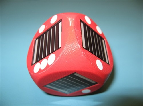
For an example of such a sensor, see the solar-powered dice in Figure 1. Using six solar panels, the dice operates entirely off of harvested light. The basic lighting in almost any room is sufficient to power the devices included in a sensor node like this.  These include an ultra-low-power: accelerometer, CC430 transceiver and of course a power supply.

The solar dice is an ultra-low-power optimized sensor node in the IoT.

Figure 1. The solar dice is an ultra-low-power optimized sensor node in the IoT.

When the dice is rolled, the system wakes up and transmits data to a universal serial bus (USB) dongle on a PC. What data, you might ask? The orientation of the dice, of course. Knowing this allows you to know which number was rolled based on which side is up. The only downside is that it reports this data after the dice is rolled and not before. Otherwise, this type of sensor node would come in very handy for placing bets, if used in casinos all over the world.

How does this dice relate to your sensor nodes you might ask?  The solar dice is just an example of what you can do with ultra-low power optimized devices to sense something and report this something back to you. But, for example, if you are designing a satellite, it’s directly applicable as you need to know which way you’re pointed (orientation) and don’t have the luxury of being plugged into the grid (you need energy harvesting). 

If you think about measuring vibrations in a car, an ultra-low power concept of the solar dice could allow smaller gauge wires to be used (which are cheaper and lighter) to power each sensor.  As well, fewer wires may be required since the data is transmitted wirelessly.  Swap out the accelerometer with a vibration sensor, and your sensor node is complete.

What types of sensors would you like to unplug using the solar-dice concept?

Additional resources:

Performance comparison between two automotive knock sensors

$
0
0

Engine knock sensors are used to improve engine efficiency and performance by monitoring engine vibrations.  The engine control unit (ECU) uses this data to adjust the fuel and air ratio to reduce “engine pinging” and correct the timing of the engine.  TI’s TPIC8101 serves as a signal conditioner for such engine knock sensors. Newer solutions sometimes integrate this functionality into one of the MCU’s in an engine’s ECU, however, this means that the processing might be done more remotely (due to the lower temperature grades of microcontrollers) which can degrade the signals.  The TPIC8101’s performance can be validated by looking at how well the signal from the knock sensor is extracted compared to the noise of the system.

Brief Theory of Operation:

The TPIC8101 performs the signal conditioning of knock sense elements, which are resonant piezoelectric sensor elements.  After passing through input amplifiers, noise is filtered out of the signal with a band-pass filter centered on the center frequency of the sense element.  The signal is then rectified and integrated.  This output can then be transmitted either digitally or through an analog signal.  The ECU monitors the strength of this signal to determine when a knock occurs.

Figure 1: TPIC8101 Internal Block Diagram

One of the purposes of the knock sensor signal conditioner is to reject all out of band noise since the engine is already an inherently noisy environment.  For this reason, the signal-to-noise ratio (SNR) that the system provides is very important.  Specifically, the band-pass filter dictates how well noise is rejected form the system. To measure the performance of the band-pass filter, the following steps must be performed.

  1. Choose the parameters such as bandpass filter center frequency, integration time constant, amplifier gain, and integration time window as explained in “Section 9.2.2” in the TPIC8101 datasheet.  These should be set according to the system level requirements, or the values in the example test settings in Table 1 can be used.
  2. Use a function generator to generate a sine wave at the specified frequency and amplitude to mimic the output of a knock sense element.
  3. Record the Peak voltage of the  signal.
  4. Adjust the frequency of the input signal and re-measure the  signal.

The plot of the output voltage ( versus input frequency will then be generated and from this, the relative SNR values of the band-pass filter is observable.

Test Data:

This test data compares the TPIC8101 and a competitor’s device to show how the differences in band-pass filters affect the device performance and SNR. Both the TI device and competitor’s device were configured the same way as shown in Table 1. 

Table 1: Test Settings

Byte

Data

Configuration

Value

Configured as

1st

0100  0110

Prescaler

11

8MHz

2nd

1110  0001

MUX

1

Ch2

3rd

0010  1001

BPF

41

6.94Khz

4th

1100  0000

Integration Time Constant

0

40uS

5th

1010  0010

Amplifier Gain

34

0.381

 Table 2 shows test data of the amplitude of the output signal with input signals of various frequencies.  Each device’s band-pass filter is programmed to have a center frequency of 6.94kHz, so input signals farther away from this center frequency should be rejected.

Table 2 : Test data


Amplitude (V) at 1KHz

Amplitude (V) at 3KHz

Amplitude (V) at 6KHz

Amplitude (V) at 7KHz

Amplitude (V) at8KHz

Amplitude (V) at10KHz

Amplitude (V) at50KHz

TPIC8101

Max

0.53

1.12

3.36

3.84

2.72

2.04

0.6

Mid

0.4

0.76

1.84

2.32

1.84

1.4

0.47

Min

0.34

0.68

1.44

1.84

1.36

1

0.4

Competitor’s Device

Max

0.5

0.5

2.52

2.88

2.08

0.72

0.5

Mid

0.3

0.25

1.16

1.6

1.22

0.06

0.2

Min

0.04

0.04

0.56

1

0.48

0

0

 The formula for SNR is:

Figure 2 plots the results from Table 1.  The noise level () is approximately the same between the two parts because the amplitude far away from the center frequency is about the same.  At the center frequency, the TPIC8101 has a higher amplitude (, meaning that its SNR is better than the competition.

Figure 2: Test Results – Amplitude vs Frequency Comparison with Competition

Summary:

The band-pass filter is a critical component of the TPIC8101.  It is easily tested and can serve as a benchmark comparison between two similar devices.  The test data shows that the TPIC8101’s band-pass filter rejects noise very well and compares favorably to competition.

See also:


Be social, discuss energy harvesting (on Twitter) live!

$
0
0

 Learn more about energy harvesting during our hour-long Twitter chat on July 8 and July 10 from 10 a.m. to 11:30 a.m. CDT (17:00 – 18:30 CEST). William Cooper, one of our product marketing engineer from MSP, will be joining other TI gurus to tackle the latest trends in energy harvesting technology and designing your own products.

Join the conversation by using #energyharvesting. We are also taking questions before the chat, so leave a comment here or Tweet us @TXInstruments.

For more information visit our Facebook event page and all the details on this upcoming event can be found on TI’s Fully Charged blog.

Let us know if you have any questions!

TI-RTOS power management features: The Inside Story

$
0
0

 TI-RTOS power management sets the standard for low-power microcontroller (MCU) applications. We are excited to announce two new videos that will enable you to learn more about this technology. The first video provides an architectural overview of the power management features and how they work. You will learn what tick suppression is and why it’s critical in low-power applications before diving into a detailed overview of the TI-RTOS power management framework that explains how it delivers state-of-the-art low-power performance without the need for the developer to do any programming or learn complex device-specific power down sequences.

The second video consists of a TI-RTOS demonstration that takes you through some of the basics of using TI-RTOS before concluding with a section on how to reduce power consumption. This will show some useful tips in addition to using both the TI-RTOS power manager as well the Energy Trace tool to show power consumption.

If you would like further information on TI-RTOS power management, you can download the TI-RTOS power management white paper.

Inductive sensing: Improve the ENOB of a multichannel LDC by 4 bits in 3 simple steps

$
0
0

In a recent inductive sensing blog post, I introduced the new new multichannel LDCs: the 12-bit LDC1312 and LDC1314 and the 28-bit LDC1612 and LDC1614.

There are scenarios in which you might want to use the 12-bit LDC1312 or LDC1314 due to higher sample rates or lower cost, when the resolution of the 12-bit LDC isn’t quite high enough for your particular system needs, for example in this 1-degree dial. In this case, you can use the gain and offset registers to improve the effective number of bits (ENOB) by up to 4 bits. Measurement timing is unaffected by using gain and offset.

The gain/offset feature works because the LDC1312 and LDC1314 have an internal 16-bit data converter, but they only display 12 of those bits in the data registers: DATA_CH0, DATA_CH1, DATA_CH2 and DATA_CH3. By default, the gain feature is disabled and the DATA registers display the 12 most significant bits (MSBs) of the 16-bit word. However, it is possible to shift the data output; see Figure 1.

Figure 1: Conversion data output gain

Employing the gain of 4x, 8x or 16x causes a 2-bit, 3-bit or 4-bit data shift, which is equivalent to increasing the maximum effective number of bits by 2 bits, 3 bits or 4 bits, respectively.

Let’s use a simple example to illustrate how gain and offset work. The example uses an LDC1314 evaluation module. My target is a U.S. quarter that moves between a 0.2mm target distance and an infinite target distance.

Here’s how to optimize the resolution in three simple steps:

  1. Determine system boundaries. When moving the quarter between the minimum target distance (0.2mm) and maximum target distance (infinite), I measure the following (Table 1):

Table 1: ENOB before applying gain

Using the gain feature discards the MSBs; therefore, it’s important to ensure that the maximum output scale does not go below zero or above the full scale of the new data output. The datasheet shows that the maximum output range must be:

  • ≤ 100% of full scale with gain = 1x
  • ≤ 25% of full scale with gain = 4x
  • ≤ 12.5% of full scale with gain = 8x
  • ≤ 6.25% of full scale with gain = 16x

 2. Apply gain. The full-scale data word is 212-1 = 4,095. My example shows a delta of 90 codes between the minimum and maximum target positions, which is only 2.2% of full scale. I can therefore comfortably use the maximum gain setting of 16x. Under this condition, I measure the following (Table 2):

((*) signal is clipped

Table 2: ENOB after applying gain

My code delta has improved greatly, but the data output at the minimum target distance clips at the full scale of my new data word.

 3. Subtract offset. While my system only uses 2.2% of full scale, it crosses the full-scale boundary, which results in a loss of information. To fix this issue, I can use the offset register to subtract a fixed offset from the data output. The maximum target distance output code is 3,212, so I can easily subtract 2,000 codes.


(*) signal is clipped

Table 3: ENOB after applying gain and offset

With a gain of 16x and an offset of -2,000 codes, the LDC now records data between 1,212 and 2,670, as shown in Table 3. This is well within the output-code limits of 0 to 4,095. The code delta is 1,458 codes, which is a 4-bit improvement over the default case with a gain of 1.

Figure 2 shows the operating output range for this example without gain, with a gain of 16, and with a gain of 16 and an offset of -2,000.


Figure 2: Conversion signal range increases after applying gain and offset

What if the resolution is still insufficient?

In this simple example, the effective resolution improved by 4 bits (from 6.5 bits to 10.5 bits) without any impact on timing or power consumption. If this effective resolution is still insufficient for your system, consider using one of our 28-bit multichannel devices, the LDC1612 or LDC1614.You can read more about the resolution benefits of the the LDC1612 and LDC1614here.

Leave a note below and let me know future topics you’d like for me to discuss about multichannel LDCs.

Additional resources

Rise of the Drones

$
0
0

2015 is quickly becoming the year of drones. So what exactly is a drone? According to the Federal Aviation Administration (FAA), a drone is an unmanned aircraft system comprising the unmanned aircraft (the drone) and all of its associated support equipment: control station, data links, telemetry, navigation equipment, etc. To fly a hobbyist drone (weighing less than 55lbs), you don’t need the FAA’s approval, as long as you keep it within your line of sight and away from populated areas/full-scale aircrafts. Flying a drone for business purposes does require FAA approval.

According to CBInsights, as of May 31, drone startups have raised more funding in 2015 than the previous three years combined (Figure 1). While the defense industry has used drones for more than a decade, they are coming into their own in the commercial space.

Figure 1:  Drone Investment activity reported by CBInsights

So what exactly is a drone? A drone is an unmanned aircraft. An unmanned aircraft system is the unmanned aircraft (drone) and all of the associated support equipment such as control station, data links, telemetry, navigation equipment, etc. To fly a hobbyist drone that weighs < 55lbs, you don’t need FAA’s approval as long as you keep it within your line of sight and away from populated areas/full scale aircrafts. But, to fly a drone for business purpose, you do need to obtain FAA’s approval .

What makes drones so attractive for business purposes? They have certain unique abilities that are opening up new applications and markets every day. Drones can overcome terrain challenges and are deployable anywhere. They can also carry flexible payloads (the lighter the load the longer the flight time) and can measure and record everything in their path from an aerial perspective. The convergence of advanced smartphone software and processing capability; very high-resolution, lightweight video-capturing equipment; and advanced flight-control algorithms are unlocking new possibilities for drones.

Commercial applications include:

  • Camera drones – to capture extreme sport enthusiasts’ adventures.
  • Agriculture – noted as having the highest potential commercially. Drones further the precision-agriculture movement by identifying and applying pesticides and fertilizers exactly where they are needed, which is better for the environment and the farmer’s bottom line.
  • Search and rescue – thermal-imaging cameras can locate missing people when the general search area is known.
  • Surveying/geographic information systems (GIS) mapping.
  • Unmanned cargo delivery – delivering that last-minute anniversary gift or your favorite pizza.
  • Riot-control drones – loaded with pepper sprays or paintballs designed to disperse crowds. (This one makes me uneasy.)

One of the challenges with drones is the flight time. Could you imagine having to stop a search effort or your pizza not making it all the way to your house due to low battery? Limited flying time in every application scenario leads to a less desirable outcome.  Although there are a few gas-powered drones, most are powered by lithium-ion (Li-ion) or lithium polymer (LiPo) rechargeable batteries. The many ways to extend flight time include making the payload as light as possible, flying in the right weather conditions, and choosing a higher capacity/higher-cell-count battery pack. Mainstream drone batteries have evolved from 3-4 cells in series to higher capacity greater than 5 cells in series. TI has a variety of battery chargers, gauges and protectors to cover the spectrum of drone application needs, including a device that can perform charging, gauging and protection all in one package – the bq40Z60.

That was a quick overview of drones, their applications and outlook. Even though every new generation of drone increases run time, you always want to remember to carry an extra battery pack or two so the fun can continue uninterrupted. Stay charged!

To learn more about TI’s battery management portfolio, please visit www.ti.com/battery


TI commends final passage of Trade Promotion Authority

$
0
0

TI AvatarWe are pleased with today’s vote on Trade Promotion Authority (TPA) as a reaffirmation of our nation’s resolve to engage and lead in the global economy.   We commend the strong leadership of the President, the House and Senate leadership and the many Senators and Representatives who have worked tirelessly to restore our nation’s ability to shape the rules governing international trade.   

TPA ensures a thorough review of future trade agreements to make sure that they advance the interests of U.S. employers, their workers and their communities.   For our company, whose revenues are driven by exports and whose operations and customers span 35 countries, this is a very welcome result.

Learn more about why we support open trade and how TPA will help to boost growth in the technology industry.

Power Tips: How to create an adjustable output power supply

$
0
0

The output voltage of a power supply is usually a fixed voltage, but sometimes it may be necessary to adjust that output voltage. For example, you may be able to reduce the power dissipation in a low-voltage high-current processor – while still keeping performance high – by adjusting the voltage fed to the core.

Adaptive Voltage Scaling (AVS) is a technology that provides this function and it’s becoming an increasingly popular feature of new processors. The “Adaptive Voltage Scaling Power Supply for Communication and Enterprise Storage ASIC Core Rails” TI Design reference design (PMP10488) is an example that would provide this functionality. Figure 1 shows the schematic for this design..

 PMP10488 schematic

Figure 1: PMP10488 schematic

The TPS53355 is a synchronous buck converter with integrated field-effect transistors (FETs); it generates a 20A output power supply from a 12V source. The design uses TI’s DCAP™ IC technology for the output control. This control strategy is well suited to an AVS application because of the improved transient capabilities. The integrated FETs allow you to optimize performance inside the IC for improved efficiency and easy board layout. The output is adjustable from 0.67V to 0.95V.

The LM10011 voltage programmer controls the output voltage. This IC takes a four-bit digital signal from the processor and generates an analog current, which you can then inject into the feedback node in order to adjust the output voltage. Because the feedback voltage is fixed at the reference, the output voltage is adjustable according to Equation 1:


In this specific example, the output-voltage range you’ll need to control is from 0.67V to 0.95V. The LM10011 has a current-source output from 0 to 59.2µA.

Using the two extremes, you can write two equations and solve for both the high-side and low-side resistor values.

Taking into account tolerances and using 1% resistor values, RTop= 5.11K and RBot= 8.66K. These values give voltage set points of 0.954V and 0.652V.

Table 1 lists measured data using the PMP10488 board.

 Output voltage versus digital-input signals

Table 1: Output voltage versus digital-input signals

Using AVS allows the processor to optimize the core voltage, thus improving performance and reducing power dissipation. This is just one example of how to create an adjustable-output power supply. For more information, see my latest Power Tips post on EETimes.

Additional Resources: 

Read the full Power Tips blog series

Glimpse into the Electrical Grid – Part 1: Introduction

$
0
0

Ever wonder how electricity gets to your home?

The electricity generation, transmission, distribution and control networks make up the electrical grid. Electric power transmission is bulk transfer of electrical energy from generating power plants to substations. Electricity is transported over long distances at high voltages, minimizing the loss of electricity. Electric power distribution includes the local wiring between high-voltage substations and customers. Combined, these form a network known as the “power grid”.


Photo credit: https://anjungsainssmkss.files.wordpress.com/2011/07/electric_grid.gif

The basic process

  1. Electricity is generated at power plant by huge generators. Power plants use coal, gas, water or wind
  2. The generated voltage is stepped-up and transmitted over high-voltage transmission lines that stretch across the country
  3. It reaches a substation, where the voltage is lowered  for distribution
  4. It travels through distribution lines to the neighborhood, where smaller pole-top transformers reduce the voltage again to take the power safely to use in homes
  5. It passes through a meter that measures how much energy a home uses  to the wall outlets

Components along the power (electrical) grid are summarized below

System Component

Function  

Voltage classification

  • Generation  - MV (Medium Voltage)  :  10 kV- 25 kV
  • AC Transmission:
    • High voltage (HV):  69 kV, 115 kV, 138 kV, 161 kV, 230 kV
    • Extra-high voltage (EHV): 345 kV, 500 kV, 765 kV
    • Ultra-high voltage (UHV): 1100 kV, 1500 kV
  • MV (Medium Voltage) Distribution: 1.1kV to 72.5 kV
  • Consumers LV:   up to 1000V
  • Direct-current high voltage (dc HV): ±250 kV, ±400 kV, ±500 kV

Inputs for power generation

Electricity generator uses fossil fuel power, nuclear power and renewable resources such as hydroelectric dams, solar photovoltaic systems, wind turbines, and biomass.

Generation (AC power supply )

Generators transform the energy of heat, wind, solar and water to electrical energy. Power is generated by large and smaller generation facilities. At generating stations, electricity is typically produced at less than 25  kV. Before entering the transmission lines, the electricity is “stepped-up” to high voltages by Step-up transformers.  

Electrical substations

Power is generated comparatively in lower voltage levels. It is economical to transmit power at higher voltage levels. Distribution of electrical power is done at lower voltage levels. For maintaining these voltage levels and for providing greater stability, a number of transformation and switching stations have to be created in between generating stations and consumer ends.  These transformation and switching stations are generally known as electrical substations.

Based on their functions, Substations can be classified into 

  • Step-up / step-down  transmission , Sub-transmission  substation
  • Distribution substation
  • Underground Distribution substation
  • Kiosk substation/indoor substation

 Transmission

Moves electricity at high voltage from generators to local Sub-transmission and distribution system. Transmission lines could be:

  • Overhead transmission lines
  • Sub-transmission Lines
  • Underground transmission lines

Transmission substation

A transmission substation connects two or more transmission lines and contains high-voltage switches that allow lines to be connected or isolated (also referred to as a switching station). The substation may have transformers to convert between two transmission voltage levels or equipment such as phase angle regulators to control power flow between two adjacent power systems. 

  Sub-transmission

Moves electrical energy at medium voltage from transmission system to distribution system. Sub-transmission lines carry electricity at voltages less than 200 kV, typically 66 kV or 115 kV.  They can also be placed underground.

  Distribution

From the distribution substation, electricity is transferred to industrial, commercial and residential customers through Distribution Lines.

While some high volume electricity users have specialized substations on their premises, retail consumer relies on local power distribution systems.

Distribution substation

A Distribution substation reduces voltage from the high-voltage transmission system to a lower voltage suitable for the local distribution system of an area. It is uneconomical to directly connect electricity consumers to the high-voltage transmission network, unless they use large amounts of energy. Distribution substations are generally located closer to the consumers.

Equipment for protection & control , communications, power quality , testing and maintenance


The following category of equipment are utilized along of the grid:

  • Primary , switching  and secondary equipment
  • Distribution static compensator
  • Protection and monitoring systems
  • Energy measurement and power quality analyzers
  • Safety  , surveillance and security  systems
  • Communication gateways and switches  ,
  • Remote management  systems
  • Fault recording  and  data logging 
  • Battery and backup power supply
  • Partial discharge  and cable fault locating equipment

Operators : Utilities

The following Utilities/Operators manage the grid

  • Distribution System Operator (DSO),
  • Distribution Company (DisCO),
  • Transmission System Operator (TSO),

Consumers, revenue  metering  

Electricity consumers are divided into classes of service   (residential, commercial, industrial, and other) based on the type of service they receive. The type of meter installed and the rates are also dependent upon class of the service sector.

Power losses :  Technical ,  commercial


Losses in the grid are mostly composed of resistance losses occurring in the transmission lines and of so-called corona losses created on the surface of conductors in certain weather conditions. The technical losses are due to energy dissipated in the conductors and equipment used for transmission, transformation, sub- transmission and distribution of power. These technical losses are inherent in a system and can be reduced to an optimum level.  The commercial losses are caused by pilferage, defective meters,   errors in meter reading and unmetered supply of energy.

Smart grid

The gradual increase of electricity cost, inadequate infrastructure, electricity losses, carbon footprint and climate changes are some of the major player for shift towards a smarter grid. The smart grid is the next generation grid network that promises advantages such as decentralized control, digitalization, flexibility, intelligence, resilience and sustainability.

TI’s role

Product  & solutions :

  • TI has products and solutions for many of the above systems which includes Digital, Analog, Interface, RF and Power.
  • TI Support: Product portfolios are supported by TI Design reference design libraries (subsystem design) and extensive collaterals.  Grid infrastructure is even a focused sector for TI with dedicated support
  • To learn more about TI’ role in the grid, visit www.ti.com/smartgrid


What are you sensing? A novel approach for capacitive-based liquid-level sensing

$
0
0

Various methods have been used to determine the liquid-level height in containers, but recently, capacitive sensing has become popular due to the accuracy and resolution of the measurements. If you have designed with capacitive-based liquid-level sensing, you may have experienced false measurement readings when you move your hand closer to your system. This is caused by the conventional capacitive technique’s limitations with robustness, especially with any external parasitic capacitance interference such as a human hand. As an example, think of a coffee maker that uses liquid level sensing to determine the amount of water required for each cup of coffee. To make the perfect cup, you need the right amount of water. If a person interacts with the coffee maker while it is running, the parasitic capacitance interference from the human body will disrupt the coffee mixture.

In this post, I’ll talk about the conventional method of liquid-level sensing, and a novel approach TI has come up with a called the out-of-phase (OoP) technique, employing the FDC1004 capacitance-to-digital converter. It provides the necessary barrier to minimize any interference, while maximizing the signal-to-noise ratio and overall robustness of the system.

Figure 1 shows the typical liquid-level sensing application setup.


Figure 1: Liquid-level sensing setup

The conventional method

The conventional method uses the parallel fingers topology: one electrode driven with the excitation signal and a second electrode connected to ground (GND), as shown on the left in Figure 2. The issue with a GND-referenced electrode is that the water has a voltage potential difference. When the hand approaches the container with the liquid, an additional parasitic capacitance is introduced into the model and the self-body capacitance directly couples to the potential difference of the water. This results in false-measurement deviations and system inaccuracy.


Figure 2: Conventional method versus OoP method

The OoP technique

The OoP technique relies on a symmetrical sensor layout, and also uses the shield drivers on the FDC1004 capacitance-to-digital converter in a unique way to counteract the effects of human-body capacitance and stabilize measurements. With the OoP technique, the liquid potential is kept constant during the excitation/drive phases by using a differential capacitive measurement, thus eliminating human-body capacitance effects from the measurements. Instead of using a GND electrode, the CINx electrode is paired with a SHLDy electrode. CINx and SHLDy have the same waveform but are 180 degrees out of phase; this is possible by setting the FDC1004 in a differential-mode configuration.

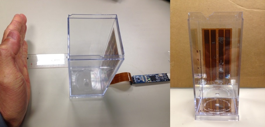
I collected hand-interference capacitance measurements with the capacitive-based liquid-level sensing TI Design reference design and compared it to the conventional method with electrodes the same size. Figure 3 shows the test setup, with the reference design on a container and connected to the FDC1004 evaluation module (EVM). Table 1 shows the capacitance measurements at a water-level height of 5cm, with the human hand a fixed distance away from the front of the container. When the hand is directly touching the container (a 0cm hand distance), the conventional method has a change in capacitance from the baseline reading (no hand present in the system) 20 times larger than the OoP technique. The calculated level absolute error dropped from about 9% to about 0.4% with the OoP technique. Over the full range of the system (0-8cm level heights), the overall absolute error of the OoP technique is about 0.5%.


Figure 3: Test setup with the capacitive-based liquid-level sensing TI Design reference design

Table 1: OoP and conventional liquid-level technique comparison

 Robustness with any capacitive-based liquid-level sensing system is important for reliability and accuracy. The OoP technique mitigates the effect of any external parasitic capacitance compared to the conventional method. A sensor layout that is as symmetrical as possible will maximize the performance of the technique.

 Additional resources

A small and innovative solution for big machinery

$
0
0

Some of our most inventive products emerge from solving a specific customer problem. That is exactly what prompted the development of the PGA900 signal conditioner– a product released this week.

TI AvatarIn late 2012, a customer came to us with a problem. Their heavy machinery, such as forklifts and bulldozers, required the customer to replace hydraulic pressure measuring equipment, including the signal conditioner, every 10 years. This pressure measurement technology is used when hydraulics are involved, such as when a forklift driver activates a lever to lift the front end of the forklift off the ground.

The customer needed a solution that lasted twice as long and with better performance, accuracy, reliability and integration – all while using less power.

This challenge pushed our engineers to think differently. Traditionally, a signal conditioner is a single analog chip within a much larger chain of analog and digital devices. A pressure signal would come from one sensor, and the signal conditioner would make the data more accurate, before ultimately sending the information to a central processor that would convert the raw information into usable, digital data. But what if the signal conditioner could do much of the “heavy lifting,” processing the information into digital data, so the central processor only needed to read the data?

“The customer wanted best-in-class performance with a really good processor, robust power management and high-performance analog input and output,” said enhanced industrial manager Robert Schreiber. “Before the PGA900, that meant putting the best-in-class in each of those products onto a single board, which results in a large board using lots of power. But this customer wanted more – an all-integrated system that simultaneously reduces power consumption and form factor, which also reduces the cost.”

That’s when Robert was brought in to lead key experts on processors, power management and high-performance analog products – engineers working in different business units all over the world. Robert’s core team reached out to the best engineers in each of these key areas to collaborate on turning the customer’s dream into a reality.

“It was a very technically challenging project,” he said. “Nothing was in place to pursue the project. No design, no verification, no applications, no test, no product engineering.  But one of the great strengths of TI is the ability to marshal resources to address a specific problem.”

The team worked closely together, and with the customer, focusing not only on the specifications requested but factoring in how the product would be used in the real world. Two years of hypothesizing, testing and refining resulted in the PGA900– a fully integrated signal conditioner offering high performance and precision without compromising power or size. It is an innovation that only could have happened by bringing experts in their respective fields together.

“Once we had a ‘dream team’ assembled, there was no discussion about whether we could do it. They just said, ‘This is fun and challenging’ and worked until the challenge was overcome. When we came up against a roadblock, we were forced to innovate around it and challenged each other internally,” Robert said.

While the PGA900 was invented for a specific use, the product can now be used in a variety of applications to measure not just pressure but also weight and load, liquid levels, strain on products, humidity, acceleration, temperature and position in factory and building automation equipment, vehicles, intelligent sensor networks, HVAC systems and white good appliances.

“This is what happens when we set our talent free and let the best engineers drive a project,” Robert said. “And it shows what happens with brilliant collaboration.”

For more information on the PGA900, please read our article in the Analog Applications Journal and our Application Report.

Enhance your university courses with hands-on LaunchPad MOOC resources

$
0
0
Massive Open Online Courses (MOOCs) are gaining traction with university students and professors, especially in countries where equivalent academic programs may not be available. The resources available from online courses are not only being utilized...(read more)

Four ways to improve your ADC system power supply rejection

$
0
0

OK so power supplies are important – what more can I do?

My previous post explained the impact that power supply variation and noise can have on analog-to-digital converter (ADC) performance. Thankfully, your data acquisition systems are not doomed. Here are four steps that you can take to ensure that your ADC is less susceptible to variation and noise in your power supplies.

1. Choose an ADC with a good power-supply rejection ratio (PSRR). Of course, the best way to protect your system performance from its power supply is to choose an ADC with sufficient PSRR to begin with. If the ADC you’ve chosen does not quite meet your PSRR needs, you can increase system PSRR by adding a high-PSRR low-dropout regulator (LDO) after your original switching supply source. This will help clean up any remaining ripple and directly add to the total system PSRR. Take a look at high-PSSR LDOs like the 3-V to 36-V, 150-mA, ultra-low noise TPS7A4901.


Figure 1: TPS7A4901 added to improve power supply rejection


2. Proper decoupling and filtering. Power supply decoupling generally takes place at two points in the system: at the supply source and at the device supply pins. Larger “bulk” decoupling capacitors (typically 1μF and above) are often placed directly at the supply output and connected to ground. This helps stabilize the supply and immediately filter as much of the supply noise as possible. Sometimes, you can place extra bulk capacitors closer to the ADC pins if you expect the current draw to be large.

Place additional smaller or “local” decoupling capacitors (typically 1μF and below) closest to the ADC supply pins to help filter away any noise picked up along the way. Using two local decoupling capacitors (i.e. 1μF and 100nF) in parallel will provide low impedance over a wider frequency range.


3. Pay attention to layout. Treat the routing of your power supplies like all other important analog signals. You want to provide the most direct and least inductive path from the supply source to the ADC supply pins. If you cannot use power planes, keep the traces short and direct, yet wide enough to handle the expected current flow. Route supply traces directly over a ground plane to allow the return current to get back to the source as easily as possible.

Figure 2: Layout example of local decoupling capacitors

Low inductance is especially important when dealing with transients. High inductance could “choke” the supply when the ADC demands a sudden increase in supply current, such as during power-up. If there is any inductance between analog and digital grounds, a transient may produce a voltage difference between them that exceeds the absolute maximum ratings, causing permanent damage to the ADC. Figure 3 shows that some devices, like the ADS1278, have a very tight restriction on the allowable voltage difference between AGND and DGND.


Figure 3: Absolute maximum rating for ADS1278 AGND and DGND


4. Be aware of certain power supply frequencies. If power supply noise does find a way past the filtering and decoupling, delta-sigma ADCs have one last line of defense: the digital filter. One of the most important functions of the digital filter is to attenuate out-of-band signals; however, the filter response repeats itself and returns to 0dB at multiples of the modulator sampling frequency (fMOD). Power supply noise near these frequencies can alias back into the signal bandwidth of interest.


Figure 4: Sinc-3 filter response out to 4 x fMOD in the ADS1298 (a) and simultaneous 50Hz and 60Hz rejection in the ADS1220 (b)

If you must use a switching power supply, synchronize it to an exact multiple of the output data rate. Depending on the filter response, the tone at the switching frequency will either fold back to DC or will be attenuated by the filter notches. Some precision ADCs, like the 24-bit ADS1220 and ADS1248, include additional filter notches at 50Hz/60Hz for select output data rates.

I hope that parts 1 and 2 of this blog series gave you a high-level understanding of how power supplies can affect ADC performance and how to mitigate their impact in your system. Remember to pay more attention to the design of your power supplies next time!

Additional resources


Four considerations when choosing a sensing solution for liquid-level measurement

$
0
0

Let’s say you need to measure the level of a liquid in a tank: perhaps it’s for an automotive gas tank, wiper-washer fluid tank or engine coolant tank. Possible solutions include traditional mechanical or electronic sensing devices.

If you have already decided to use electronic sensing, you still have other choices to make. Electronic capacitive sensing works well for many liquid-level sensing applications, but the unique conditions of automotive applications may require a different approach. To determine the best solution for your application, you need to do some information gathering. You will need to answer four key questions:

  1. What are the properties of the liquid you’re monitoring?
  2. Will you measure the liquid from inside or outside the tank?
  3. What are the conditions of the tank?
  4. What are the accuracy requirements of your system?

Question 1: What are the properties of the liquid you’re monitoring?

Is the liquid viscous, corrosive, homogenous? Corrosive liquids such as urea and alcohol make it increasingly difficult for mechanical devices to measure liquid levels since they typically need to come in contact with the liquid itself. On the other hand, capacitive- and ultrasonic-sensing methods do not come in contact with the liquid since both of these methods allow you to monitor the level of the liquid from the outside of the tank. With capacitive sensing, pairs of conductive plates running down the side of the tank will monitor the level. Ultrasonic sensing involves mounting a piezo sensor on the bottom of the tank. Both methods are noninvasive and not negatively impacted by corrosive liquids. However, liquids that are viscous in nature (power-steering fluid, brake fluid, engine oil) leave a film on the inner wall of the tank when the level goes down; this can be problematic for capacitive sensing.

Question 2: Will you measure the liquid from inside or outside the tank?

One method for measuring fluid level from inside the tank is a resistivity technique. However, this becomes problematic with corrosive liquids. Due to reliability, cost and limitations of internal level-sensing techniques, external electronic-sensing devices such as ultrasonic and capacitive are gaining in popularity for automotive applications. You have fewer choices if the tank is metallic; since capacitive sensing relies on an electric field to make its measurement, it’s not an option here.

Question 3: What are the conditions of the tank?

More than likely, your tank is made of high-density polyethylene (HDPE) or steel. Mechanical devices such as a moving “float arm” can internally monitor liquid levels in tanks of all different materials. However, they have mechanical limitations when the shape of the tank is irregular (something other than a cylinder or rectangular in nature) or if the tank is very tall and thin because they limit the float arm’s capability.

Question 4: What are the accuracy requirements of your system?

While some mechanical devices can achieve accuracies in the single percentiles, capacitive- and ultrasonic-sensing solutions can generally achieve millimeters of accuracy. Capacitive sensing achieves this by having a pair of electrodes below the minimum surface of the liquid and another pair that runs the full height of the tank. If system conditions vary greatly, you may need another pair of electrodes above the liquid level as well. In the case of ultrasonic sensing, a single piezo transducer is sufficient to achieve better-than-millimeter accuracy by applying a time of flight (TOF) measurement technique.

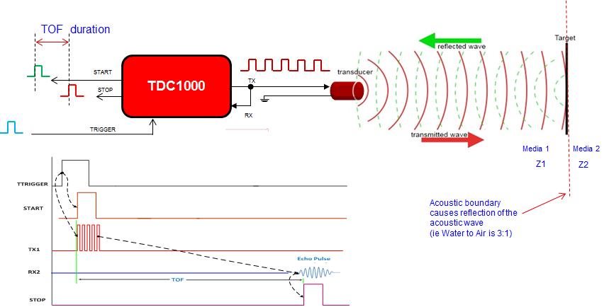
Ultrasonic TOF level measurement works by using a single piezoelectric transducer to create a pulse from the bottom of a tank, as shown in Figure 1. The pulse travels through the tank wall and into the fluid in the tank. It continues to propagate through the fluid until it reaches the fluid surface that represents a large change in acoustic impedance. Due to the large change in acoustic impedance at the fluid surface (fluid to air interface), an echo is created, and the sound wave propagates back toward the piezo transducer. Measuring how long it takes for the echo to return to the transducer is referred to as TOF.

 Figure 1: Ultrasonic time of flight level measurement

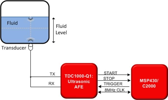
The TDC1000 ultrasonic analog front end (AFE) makes TOF measurements simple by exciting the transducer and receiving the echo. In turn, the TDC1000 creates a start and stop pulse, both of which are easily monitored by a microcontroller, which acts like a stopwatch in order to measure TOF and achieve 1mm height accuracy. This process is illustrated in Figure 2.


Figure 2: Automotive liquid-level and fluid-identification measurement system block diagram

I hope these four key considerations help you decide which sensing solution for automotive liquid-level measurement is best for your application and give you some understanding how ultrasonic sensing delivers the benefits of both millimeter accuracy and noninvasive sensing. Do you plan to use ultrasonic sensing or a different option for your next project? Leave a note in the comments section below.

 Additional resources

Autodesk’s Ember…the story behind the technology

$
0
0
Autodesk brings its Ember 3D printer to market with help from TI DLP® technology -- you can see it below When we take Ember to a show or event, it seems to attract its fair share of attention and raise questions that we love to answer. From...(read more)

USB Type-C for mobile phones: Changing the way phones connect, one flip at a time

$
0
0

Will mobile phone designers adopt all of the available features in the universal serial bus (USB) Type-CTM specification? Probably not. They’ll weigh their options against the impact on overall product cost. The new USB Type-C interface comes with ultra-thin connectors that are less than 3mm high and 8.4mm wide, making it ideal for mobile phones. USB Type-C offers a cable-and-plug assembly that is “flippable” and reversible. The interface provides options for data and video up to 20Gbps and power up to 100W.

Figure 1: USB Type-C full-featured cable

The USB Type-C interface supports USB 2.0 and 3.1 data and 15W (5V, 3A) power charging natively using a channel configuration (CC) function. The optional USB Power Delivery (USB PD) function enables video such as DisplayPort and power charging up to 100W (20V, 5A).

While USB On-The-Go (OTG) allows mobile phones to assume dual data roles – a host or a client device – USB Type-C introduces a mode called dual role port (DRP) that allows it to have dual roles for both data and power. DRP means that the port can either assume the downstream facing port (DFP) role as the USB host and power provider or the upstream facing port (UFP) role as the USB device and power consumer. As a result, a mobile phone with DRP can get power for charging when connected to a laptop or in turn provide power to a flash drive. USB PD further enables independent data and power roles so that an upstream data port can provide power and a downstream data port can sink power.

As I mentioned earlier, engineers must decide if different USB Type-C features are worth the trade-offs and potential increased cost. Some of the trade-offs may include:

  • DRP versus UFP. While most mobile platforms will implement DRP, some might stick to only UFP for a simpler implementation.
  • USB 2.0 versus USB 3.1. A typical USB 2.0 implementation will have both D+ shorted and D- shorted as stubbed connections, eliminating the need for a multiplexer (mux). Choosing USB 3.1 will require a mux to accommodate USB Type-C cable/plug flipping. For a mobile phone, USB 2.0’s data-transfer rate (-about 40MBytes per second of effective throughput) may be adequate for everyday use.
  • Alternate mode video. Apart from system support for video, a port also requires a USB PD device and a complex data mux such as a cross-point switch, increasing cost. Depending on the system design, additional signal conditioners could also be necessary.
  • 15W versus enhanced power. Native 15W power is part of the USB Type-C CC function and will not require any extra device; however, increasing power capability will require a USB PD device, adding cost. A typical smartphone has about a 6Wh battery and will take around 30 minutes to charge using native USB Type-C. A “phablet” may take about 50 minutes. This speed is six times quicker than standard USB 2.0 charging and 1.5 times than the fastest USB Battery Charging (BC) 1.2 rate.

See Table 1 for USB Type-C options for system implementations.

Table 1: USB Type-C options with a native CC controller versus USB-PD


TI’s TUSB320 is a single-chip CC controller solution for mobile phones with USB 2.0 data and 15W of power support. The device provides optional features such as Try.SNK, audio/debug accessory detection, dead battery support and ID emulation for flexible system implementations. Note that two DRPs connected together result in a random power provider/consumer relationship unless the phone becomes a power consumer using the Try.SNK feature. The Try.SNK feature could be useful to avoid situations where a phone starts charging a notebook.

If you are in need of a solution that supports both power and data requirements, TI’s TUSB321 and HD3SS3212 together can provide a USB Type-C solution that provides USB 3.1 for data and 15W for power. The TUSB321 is a CC controller with VCONN power output (required per USB Type-C specs) to support active cables. The HD3SS3212 is a USB SuperSpeed mux supporting USB 3.1 Gen 1 and 2.

TI’s TUSB320TUSB321 and HD3SS3212 meets USB Type-C Specification 1.1 Engineering Change Notices as of June 22, 2015. In addition, we’re early leaders in interoperability, providing the most robust solution for the USB Type-C ecosystem.

What would you like to know about USB Type-C in future blog posts? Let me know by leaving a comment below.

Additional resources

Motor start-up techniques: Part three

$
0
0

I have discussed sensorless motor start-up with our InstaSPIN-FOC™ technology in part one of this series, followed by a discussion of how to generate sufficient torque at start up and maximize it while spinning your motor in part 2. In this third and final part of the series, I’ll explain how to address some challenges in applications that may have highly dynamic loads up to 100 percent or rated torque output.


Continuous Angle Tracking

To truly solve the problem, you need to be able to continuously estimate the rotor flux angle at zero and very low speeds and transition between the low-speed and high-speed observers in a stable manner. A new set of libraries is being provided to make this possible with InstaSPIN-FOC technology. The library is in two parts:

  • IPD_HFI: Initial Position Detection (IPD) and High-Frequency Injection for Zero- and Low-Speed Operation
  • AFSEL: Logic transitions between IPD_HFI and FAST


Figure 1. Frequency of operation with FAST and IPD_HFI


Initial (Zero Speed) Position Detection

The IPD portion of the IPD_HFI module uses the BH curve of the iron that the stator coil is wrapped around to determine the north pole of the rotor and thus the d-axis. The magnetic field strength will bias the stator’s BH curve operating point as shown in in the below figure. Supporting and opposing magnetic fields are applied with the stator coil. When both fields support, the BH curve is pushed further into saturation. When the magnetic fields oppose, the BH curve operating point moves further into the linear region. The difference in inductance between these two BH curve operating points allows the IPD algorithm to determine where the rotor north pole is located.

Figure 2. BH curve and relative location for different rotor orientations


Low Speed Position Detection

Once the rotor’s north pole is located, for best control system performance it must be tracked at all times during the operation of the motor, even the very short time between start-up and FAST reliably being able to provide valid angle estimations. The IPD_HFI solution uses a high-frequency signal to track the north pole. However, this capability relies on the motor design having a large saliency. Saliency can be introduced by placing the rotor magnets below the surface of the rotor with gaps of the rotor’s iron left in between poles. Contrast this to a non-salient surface mounted design.

Figure 3. Salient vs. Non-Salient rotor designs


For the salient type, because the magnetic material has a much less relative permeability than the surrounding iron, the reluctance difference for flux flowing through the magnet is greater than reluctance of the iron path. As the rotor’s angle advances, the reluctance has a periodic variation. If the inductance is measured on a coil of the stator, it will look something like below:

Figure 4. Inductance variation of a highly salient rotor


The HFI part of IPD_HFI uses this information to stay locked onto the north pole of the rotor while it is spinning at low speeds. To make certain that its angle is locked onto the north pole – and not a south pole peak – the HFI is initialized to the D-axis north pole by the IPD portion. The high-frequency signal used to excite this signature is selected based on the time constant of the motor.


Transitional Logic

The HFI algorithm works very well at low speeds but it has a maximum speed limit. Before this maximum speed limit is reached, control has to be handed over to a higher speed observer like FAST. The module that selects between low-speed (HFI) and high-speed (FAST) estimators is the angle frequency select (AFSEL). AFSEL requires angle and frequency inputs from both the low- and high-speed estimators and the speed at which the control is passed from one estimator to the other. 

Figure 5. InstaSPIN-FOC with FAST (EST), IPD_HFI, and AFSEL


Limitations

Besides the need for a salient rotor design, one of the key limitations is the effect of the current through the motor on the saliency effect. To start a motor under load, enough current has to be consumed by the motor to produce the needed torque. As the currents increase the reluctance variation is diminished, hence the inductance variation is diminished, and the HFI portion will not estimate the angle location precisely enough to maximize torque production. This must be tested and is highly dependent on the motor design and the initial saliency (variation). More is always better.


Example Implementation

An example “Torque Control” implementation has been released as “proj_lab21” starting with MotorWare revision 1.01.00.14

Initially the project is just being released on the DRV8301 Rev D EVM inverter with our C2000™ Piccolo™ F28069 microcontroller. In future revisions of MotorWare™, support will be extended to different combinations of inverters and controllers as well as further system examples such as “Speed Control.” Learn more about InstaSPIN and IPD_HFI at www.ti.com/instaspin.


Selecting the right processor: WiLink 8 plug and play platforms

$
0
0

With all of the processors and platforms available today, deciding which evaluation board to develop with can be daunting. We’re hoping to ease this process with our WiLink™ 8 plug and play platform guide.

TI makes it easy to start evaluating our WiLink 8 Wi-Fi® and Bluetooth®combo-connectivity solutions with a range of different platforms to fit your design needs. The descriptions below will help guide you through the selection process to find the right evaluation platform for your design.

Sitara™ AM335x processor 

The Sitara AM335x evaluation module (EVM) enables developers to immediately start evaluating the Sitara AM335x processor family. Mounted with the TI WiLink COM8 module for Wi-Fi and Bluetooth / Bluetooth low energy connectivity, the reference platform provides the fastest connectivity ramp with software, collateral and reference applications available from TI.

Hardware

Software

Additional resources

Sitara AM335x  EVM

WiLink 8 COM8 EVM

Sitara AM335x Linux EZSDK


Sitara SDK Release Notes wiki

WiLink 8 wiki


Sitara AM437x processor 

The Sitara AM437x evaluation module (EVM) enables developers to immediately start evaluating the AM437x processor family (AM4376AM4377AM4378 and AM4379) and begin building applications such as portable navigation, patient monitoring, home/building automation, barcode scanners, portable data terminals and others.

Hardware

Software

Additional resources

Sitara AM437x EVM       

WiLink 8 COM8 EVM

Sitara AM347x Linux EZSDK


Sitara SDK Release Notes wiki

WiLink 8 wiki

BeagleBoneandWiLink 8 Cape 

The Sitara AM335x BeagleBone Black reference board with WiLink 8 cape introduces a low-cost easy to ramp solution to enable multiple customer applications such as audio streaming, home automation and more.

Hardware

Software

Additional resources

BeagleBone Black board with Sitara AM335x

BeagleBone cape with WL1835 module

Sitara AM335x Linux EZSDK

Debian Distribution

BeagleBone Black

Debian on BeagleBone

WiLink 8 wiki


“Jacinto 6” infotainment processor 

Developed on the same scalable architecture, DRA74x ("Jacinto 6") and DRA72x ("Jacinto 6 Eco”) are two members of next-generation family of infotainment processors from TI. They enable car manufacturers to scale product investments and deliver a diverse portfolio of products with software and hardware compatibility with the broadest array of ARM Cortex-A15 devices. With the OMAP 5 architecture at its foundation — including ARM® Cortex™-A15 core(s), quad Cortex-M4 cores and SGX544 3D graphics core(s) – the DRA74x and DRA72x processors bring feature-rich, in-vehicle infotainment and telematics features to the next generation of from entry- to mid-level to high-end. 

Hardware

Software

Additional resources

“Jacinto 6” EVM

WiLink 1877Q COM8 EVM

Android™ Lollipop: software

Automotive connectivity solutions overview


Additional performance EVMs and SoMs

In addition to the range of TI evaluation platforms listed above, our WiLink 8 combo-connectivity solutions are compatible with various non-TI platforms, enabling easy-to-use, easy-to-integrate reference connectivity solutions for both industrial and consumer applications. An example of one of these solutions may be viewed here.

For turnkey solutions, TI has partnered with 3rd parties to develop SoMs with TI/non-TI Host CPUs and WiLink8 modules. To list a few:

WiLink 8 firmware supports Wi-Fi and Bluetooth co-existence between both IPs, which is much needed if operating in the congested 2.4GHz band. Also, TI has partnered with module vendors to offer modules with our WiLink 8 solution and ZigBee® CC253x wireless MCUs on the same device, supporting co-existence between the Wi-Fi and ZigBee technologies. An example of this coexistence can be seen in the Partron module  CZ3130A.

Now that you’re familiar with our plug and play options, order your WiLink 8 combo-connectivity device and start designing today.

Viewing all 4543 articles
Browse latest View live