Quantcast
Channel: TI E2E support forums
Viewing all 4543 articles
Browse latest View live

“Swiss Army Knife” of audio codecs

$
0
0

Free TI Design and Optimized Codec available from TI

If you were to mention Opus to someone, the first thing that may come to mind is a penguin character from a popular comic strip, or even a set of musical compositions. But the ‘Opus’ that has recently been making waves is the Opus codec - the state-of-the-art, highly versatile, royalty-free audio codec to be standardized by the Internet Engineering Task Force (IETF).

It has been referred to by its developers as the “Swiss Army Knife of audio codecs” because it supports variable bite rates (6 kbps to 500+ Kbps) and frame sizes (2.5 ms to 60 ms) and goes from narrowband to fullband.

Source: http://www.opus-codec.org/comparison/

This makes the Opus codec useful for a range of applications from speech to high-fidelity music, with ability to span low latency voice applications such as VOIP, as well as internet streaming and storage applications. As a lossy audio codec that is available for free, Opus also has technical advantages over other lossy codecs such as Vorbis, MP3 and AAC, especially at low bit rate. Once can learn more about it at the public Opus home page.

With the C6000 DSPs excelling at implementing real time codecs, it was only natural for Texas Instruments to offer a DSP optimized version of this codec. TI also shows how to accelerate implementation of this codec with the help of a TI Design that can downloaded for free from ti.com. This TI Design implements the Opus 1.1 Codec on the TMS320C6657 high-performance DSP, based on TI's C66x KeyStone multicore architecture. Some of the included data shows how efficiently the codec runs on the C66x DSP architecture (in some cases over 3X the performance of the codec running on a general purpose processor See table below for one specific use case).


Configuration

Performance Statistics (in Peak Megacycles/sec)

C66x (optimized)

ARM® Cortex™-A15

WB

WB

Encoder – LE

14.5

45.6

Decoder – LE

2.82

12.8

Full Duplex – LE

17.32

58.4


To view more of the performance and comparison scenarios as well as the assumptions and criteria for comparison, please refer to the design guide at the TI Design site. For designers wanting to integrate their own application with the Opus Codec, the floating point performance on the dual core TMS320C6657 (up to 40 GFLOPs) offers quite a bit of performance headroom.

Take a look at the TI-optimized Opus codec and the related TI Design and see what it can do for your application. Be sure to share your success stories in the comments section below.

For a limited time, get the TMDSEVM6657LS for 50 percent off in the TI Store using promo code 6657DEAL50.


Low-power software development increases battery life

$
0
0


Battery innovation is not moving as fast as other technological advantages. With battery capacity doubling every 10 years and processing requirements increasing much quicker, developers are faced with difficult challenges. When building a battery-powered system, product developers often create efficient hardware systems only to see much higher power consumption than expected. In embedded systems optimization, hardware is only half of the equation that must be considered. The other half is software.

Microcontroller (MCU) software can be managed to ensure maximum battery performance. If you are looking to get started, consider these tips:

  1. Maximize time in standby– standby-mode current of a MCU is often orders of magnitude lower than active-mode current. This is often due to power gating of non-essential peripherals and system modules while waiting for an event to occur.
  2. Use interrupts to control program flow– This is about efficiency of code. Every line of code being executed consumes clock cycles and in turn your system battery life. Use interrupts to make intelligent decisions about what section of code to execute based on the state of a system.
  3. Replace software functions with peripheral hardware– Implementing security functions, such as encryption, can require thousands of cycles to execute in software. On our low-power MSP MCUs, 128-bit encryption can be reduced from 6600 clock cycles to 168 cycles, all by using the included hardware module. Similar performance benefits can come from simple modules such as hardware multipliers that can simplify math functions dramatically.
  4. Manage power of internal peripherals– Even if not in a standby mode, non-essential peripherals should always be turned off.
  5. Manage power of external devices– The concept of turning off non-essential components does not stop within the MCU. The MCU in a system can be used to turn components on/off when needed to maximize battery life.
  6. Device choice can make a difference– Remember, not all MCUs are created equal. Applications have varying requirements for time in active or standby mode. Choose an MCU that is optimized for your duty cycle. Also, keep in mind that wakeup time from standby modes can become an important factor if the application required moving from active to standby mode often.

Efficient software is definitely a “must” to ensure battery life maximization. The tips above should help, but there are many additional factors to consider and optimization utilities can help. If using TI’s MCUs, check out our software optimization options to help simplify your development.  To start, ULP Advisor helps check your code against an ultra-low-power checklist to provide guidance on potential software improvements. EnergyTrace™ technology then provides real-time power profiling capabilities so that you can see exactly where, and how much, power is being consumed. To learn more about TI’s ultra-low-power MCUs and software, visit www.ti.com/msp.

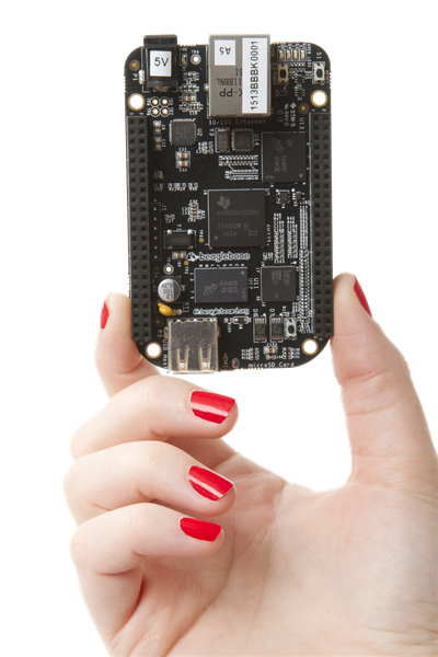
Micro Digital extends SMX® RTOS support to BeagleBone Black

$
0
0

SMX® RTOS is now available on BeagleBone Black. SMX RTOS provides deterministic real-time performance that enable developers to use it for industrial applications that have hard real-time requirements. SMX RTOS includes the smx multitasking kernel, smxNS TCP/IP stack, smxFS FAT file system, and smxUSB host and device stacks. Developers can choose only the modules they need for their application. These modules are shipped fully preconfigured and running together on the board together with the board support package (BSP). Detailed BSP notes are provided for each board that summarizes key settings in the BSP, kernel, and middleware modules and to alert about any special hardware issues. SMX RTOS has previously been released for other Sitara™ AM335x boards, such as the industrial development kit (IDK), EVM, and software development kit (SDK). It  has also been used in multiple Sitara AM335x applications.


The smx real-time kernel has an advanced architecture that incorporates numerous features that enable developers to easily meet real-time deadlines while benefiting from the ease-of-use offered by starting with a proven set of RTOS modules. Some of its key features that offer superior real-time performance include:


•             Link service routines (low overhead threads) for low interrupt latency

•             Preemptive scheduling and support for one-shot tasks and stack sharing

•             Messaging with features for safety, priority passing, broadcasting, multicasting, and block migration, as well as simple queue-type messaging

•             Mutexes with priority inheritance and ceiling protocol, which support priority propagation and staggered priority demotion

•             Semaphores of six types including event, resource, threshold, and gate.

•             Event groups that support AND, OR, and AND/OR combinations of flags.

•             Timers (one-shot and cyclical) that invoke LSRs to reduce jitter, as well as pulse timers for PWM, PPM, and FM.

•             Heap that uses bins to maximize performance and minimize fragmentation, with the ability to easily tune it for your application.

SMX RTOS has also associated debug features and tools that enable developers to more easily optimize system design and debug any multitasking-related issues. The error management system allows both local and central handling so the developer can handle and, if necessary, customize error messages with minimal effort.  The smxAware debugging tool has graphical displays for event timelines, stack usage, profiling, memory usage, and memory map overview. These views allow the developer to optimize memory use and performance to ensure real-time deadlines are being met. SMX RTOS requires IAR Embedded Workbench for ARM as the development environment and a JTAG connector must be added to the BeagleBone.

For more details on SMX RTOS features that simplify development of real-time applications, go to www.smxrtos.com/special. To obtain a SMX Evaluation Kit for BeagleBone Black, contact Micro Digital at 800 366 2491 or sales@smxrtos.com.

Program your SimpleLink CC2650 SensorTag with cloud-based development tools

$
0
0

TI's suite of cloud-based software development tools now support the SimpleLink™ CC2650 SensorTag.

By visiting dev.ti.com you can access TI's cloud-based development tool portfolio including Resource Explorer and Code Composer Studio™ Cloud integrated development environment (IDE).  Use Resource Explorer to browse through available documentation and examples.  I recommend starting with the Bluetooth Smart demo and importing it into Code Composer Studio Cloud IDE.  You can then modify the code and flash it to your SensorTag.  Connect your SensorTag to the mobile app running on your Android or iOS device to interact with your kit.

Note that in order to be able to program the SensorTag using CCS Cloud you need to have the Debug DevPack connected to your SensorTag.  This simple $15 add-on features an XDS110 debug probe that enables flashing and debugging of the SensorTag.

This short video shows how to get up and running with the SensorTag demo application and TI cloud-based software tools:

(Please visit the site to view this video)

Understanding MOSFET data sheets, Part 4 - Pulsed Current Ratings

$
0
0

Welcome back, fellow FET enthusiasts to part four of the "Understanding MOSFET Data Sheets" blog series! Today I’ll be talking about pulsed current ratings, how they are calculated, and how they are represented in the safe operating area graph on the FET datasheet.

The pulsed current rating (IDM) that appears on the front page of the datasheet, is not unlike the continuous current rating, in that it is a theoretically calculated value. However, unlike the continuous current, the IDM is only calculated as a function of thermal constraints, from normalizing RθJC to the given pulse duration and duty cycle specified in the footnote of the “Absolute Maximum Ratings” table.

Take for instance, the recently released CSD17579Q5A 30V N-Channel MOSFET. The data sheet for this part has a maximum pulsed current rating of 105A, based on the conditions that the pulse duration is less than or equal to 100µs and the duty cycle is less than or equal to 1%. To determine the transient thermal impedance to use in calculating the IDM, we will refer to the normalized thermal impedance curve, shown in Figure 1 below. If we look at the 1% duty cycle (brown) line at 100µs, we get a normalization factor of 0.12, which we will use to calculate the max power and thereby current the device can handle for this duration and duty cycle. This value is given by 0.12 multiplied by the max DC RθJC (4.3˚C/W), yielding a transient ZθJC of 0.52˚C/W.

Figure 1: CSD17579Q5A Normalized Transient Thermal Impedance CurveFigure 1: CSD17579Q5A Normalized Transient Thermal Impedance Curve

Using this value for thermal impedance and calculating the max current just as we did for its continuous counterpart, we will calculate a thermally limited current of 119A. But wait! The datasheet said 105A! So what gives? If you look at the SOA of the device, shown below in Figure 2, it can be seen that the 100us line actually bumps into the RDS(ON)  limitation before it can get to 119A. This intersection occurs at 105A. So in cases like this, we will retroactively derate the absolute maximum pulsed current as the physical limitations of the device’s RDS(ON) will limit the device from being able to reach its thermal limitation.

Figure 2: CSD17579Q5A Safe Operating AreaFigure 2: CSD17579Q5A Safe Operating Area

Current limitations are calculated for each greater pulse appearing in the SOA, and provided they don’t run into the RDS(ON) limitation first, this value is where those curves are capped.

Because the absolute maximum current is entirely theoretical, prior to release of the part we will attempt to get some hard data to further convince ourselves that the part is capable of handling this much power. Unfortunately, our best boards and testers are only capable of pulsing the devices up to 400A, which is why that value has served as an artificial cap for all devices we release. Some vendors have a similar cap, while others do not limit themselves in such a manner. While you will never see TI rate a FET beyond 400A IDM, either on the front page or in the SOA, Table 1 below shows you how ridiculously high the theoretical pulsed current rating can get, in this case for the CSD17570Q5B, a part with very low RDS(ON) (0.69mΩ max) and thermal impedance (0.8˚C/W). This demonstrates how different vendors can get away with displaying higher ratings, if they play with features such as pulse duration and ignore practical limitations of testing the device.

Table 1: CSD17570Q5B Calculated Pulsed CurrentsTable 1: CSD17570Q5B Calculated Pulsed Currents

In part five of “Understanding MOSFET data sheets,” I will provide a similar analysis for the pulsed current rating, IDM, and show how this ties into the other parameters on the datasheet, including the SOA. In the meantime, watch a video "NexFET™:Lowest Rdson 80 and 100V TO-220 MOSFETs in the World" and consider one of TI’s NexFET power MOSFET products for your next design.


Advanced charging features extend battery run time for wearables

$
0
0

The battle of the smartwatches has brought everyone’s attention to wearables again. In almost every review and technical comparison, the one thing that came up the most was battery runtime. No matter how many fancy features a smart watch has, they are useless if the battery is dead.

The battery runtime is affected by various factors including battery capacity, power consumption of the PCB components, user habits, etc. Among all of these factors, battery capacity is absolutely the most decisive one. Normally, battery capacity is in proportion to the physical size of the battery pack, which is already limited by the size of the smart watch. Of the several major smart watches on the market today, battery capacities range from 130mAh to 410mAh, and runtime is from less than one day to a couple of days. For other wearable devices such as wrist bands, Bluetooth headsets, glasses and jewelry, the battery capacity must be smaller, making each milliamp hour (mAH) critical for the battery run time.

Two parameters affect battery capacity and runtime, especially for small batteries:

Battery leakage current and charging termination current.

To demonstrate how critical battery leakage is, let’s assume that a wristband is using a 50mAh battery, which can support 30 days of operation if the IC itself consumes zero current from the battery – which is the ideal case. By adding different battery leakage currents to this model, the battery runtime will be reduced by different amounts. As is shown in Figure 1, with 75nA of leakage, there’s essentially no difference; the battery can still support 30 days of operation. With 5µA of leakage, however, battery runtime is two days shorter. With 10µA leakage, runtime is four days shorter; with 20µA leakage, the IC consumes 25% of the battery capacity. Obviously, the smaller the battery capacity, the more critical the leakage is.


Figure 1: The impact of battery leakage current on battery runtime

So why is termination current so important? We took two charge-cycle data from a 41mAh battery with the same 40mA fast charging current and two different termination currents. In Figure 2, the green line represents a normal 10% termination ratio, with charging terminated at 4mA and a charge time of 97 minutes. The red line in Figure 2 represents a 1mA termination current and a total charge time of 146 minutes. So the extra 50 minutes of charging provided an extra 2mAh, which is 5% of the total battery capacity. Is it worth it? Well, this 5% can provide as much as two more hours of operation for a smart watch.

 Again, the smaller the battery, the more critical the termination control. For a 20mAh battery, if you cannot control the termination current below 5mA, you are losing more than 10% of battery capacity even before you start using it.


Figure 2: Charge cycle for a 41mAh battery with 4mA and 1mA termination currents

There are several charger solutions from Texas Instruments that are widely used in the low power applications today, such as bq24040 and bq24232. To accommodate the special requirements of wearable applications, the bq2510x charger family was introduced. The battery leakage current is less than 75nA and the termination current can be accurately controlled at 1mA. The bq2510x’s extremely small 0.9mm by 1.6mm package size is also ideal for these space-limited low-power applications.

Additional resources

Simplifying gate driver design for brushed DC motors

$
0
0

Are you looking to drive a simple brushed DC motor? Do you need to use discrete MOSFETs to drive a bunch of current through a giant brushed motor with little time for development?

When you grab an off-the-shelf gate driver, you always see a diagram like Figure 1: just choose two resistors and you’re (theoretically) good to go.

Figure 1: A hypothetical gate-driver schematic


There’s just one problem: Figure 1 doesn’t work. The low-side FET will turn on when the half-bridge pulls high, and you will need to keep the low-side FET gate low to prevent shoot-through and damage. Instead, you end up using something like Figure 2 to make the circuit function, but then you’ll still have to slow down the half-bridge rise time. The FETs run hot because of the long switching times. So you can’t really make any improvements without adding additional components.

Figure 2: The actual gate-driver schematic


In my opinion, the worst part of the whole process is the trial-and-error resistor selection. When you have to keep soldering and unsoldering resistors, it really slows down the whole design. (Even though I personally enjoy soldering and lab testing.) It’s just very demotivating to have to make board modifications between every. single. test.

The right gate driver really makes a difference in making motors easier to spin. It can eliminate the issues I’ve described if you select the right option. A special gate-drive architecture that we at TI call “IDRIVE/TDRIVE” could help solve your problem. The architecture is called IDRIVE/TDRIVE because those are the primary parameters: IDRIVE is the gate-drive current and tDRIVE is the time during which IDRIVE is active.

Figure 3: IDRIVE/TDRIVE gate current (lesson: don’t let engineers name things)


Instead of requiring external gate resistors to limit the gate-drive current, the driver can control the gate current internally. You can set the gate-drive current by simply using a pin, or through serial peripheral interface (SPI) registers, depending on the device. You’ll see zero gate resistors on data sheets (like in Figure 4) because the devices will operate perfectly well without them.

Figure 4: IDRIVE/TDRIVE actual schematic


One of the biggest advantages of having no gate resistors is that the gate driver can apply a strong pulldown on the FET gate. When the high-side FET is turning on and the phase node is slewing up, the low side FET gate-to-drain capacitance, CGD, will couple the phase-node rising edge onto the FET gate. In Figure 1, the gate driver was limited in its ability to keep the gate pulled down. In Figure 3, this new gate-drive architecture can apply a strong pulldown to the low-side gate while still allowing a much more gentle gate charging/discharging current when you want to turn the FET on or off.

If the gate-drive current is adjustable on a pin, you can modify it by using a single resistor or with a digital-to-analog converter (DAC) forcing a voltage. If it is adjustable through SPI, you can just write a register to change the current. IDRIVE/TDRIVE allows you to modify the gate-drive current whenever you want, even on the fly as you are driving the motor.

IDRIVE/TDRIVE makes it easy to experiment with gate-drive currents in a system without having to unsolder multiple passive components between trials. Figure 5 below shows you a few plots of the DRV8701 at different gate drive current settings.

The IDRIVE/TDRIVE architecture is available on several devices right now:

  • The DRV8701 single-brushed DC motor.
  • The DRV8711 dual-brushed DC motor or stepper motor.
  • The DRV8308 brushless DC motor.


Figure 5: IDRIVE/TDRIVE gate-drive settings and associated rise times on the DRV8701 evaluation module


So go ahead and skip the frustration in motor driver gate drive design and check out the IDRIVE/TDRIVE architecture. Spend less time dealing with your MOSFETs and more time spinning your motor!


Additional resource:


Learn more about TI's DRV8701, a new brushless DC gate driver made for scalable designs. 

VIDEO: TIers bring kids to work, sparking an interest in STEM

$
0
0

From hands-on programming activities to controlling robots to drawing prototypes of what they would invent, the daughters and sons of TIers recently enjoyed an exciting day with their parents at work. As an engineer by education and the leader of our Embedded Processing business unit, I understand our future as a company depends on building the pipeline of talent to continue delivering innovations that set our company apart.

This is why an event like our annual Take Our Daughters and Sons to Work day is so important. We hope to spark the imagination in kids, showing them that engineering is not some esoteric thing. Our goal is to open their eyes a bit, giving them exposure to the real concepts that result from science, technology, engineering and math subjects.

(Please visit the site to view this video)

Not all students have parents in engineering fields, which is why we also invited a group of young ladies from Girls Inc., a non-profit organization we work with, to participate in our event. These impressionable girls received great experience with hands-on programming from our engineers, helping them see what we do in our daily jobs and what their future could possibly look like. In the past year, women comprised less than 15 percent of engineering graduates. We need more young women in engineering, and it was so encouraging to see our women engineers showing these girls what is possible.

As a parent of five children, I’ve continually emphasized that while STEM subjects may be more difficult at first, having the discipline to take these courses can help them build a foundation and allow them to do more than they ever thought possible. Also, showcasing STEM activities in fun, exciting ways at events like this, we continue to build awareness in STEM fields with our own children, as well as students in the community. You never know. One of these events could create the small spark needed to ignite a future career in engineering.


Enabling long life in dual-coin cell powered meters

$
0
0

Many smart meters are powered by two coin-cell batteries connected in series; after all, two batteries give twice as much battery life as a single battery. The second battery provides the energy required to meet the greater-than-10-year runtime between battery replacements that the industry requires.

Unfortunately, two batteries also give twice the voltage, which is harder to convert down even with the latest in ultra-low-power management devices. The higher voltage of two batteries in series is above the allowed range of many semiconductor devices, which are usually designed to accept just a single battery’s voltage.  When considering ultra-low-power devices, which are absolutely required in this application with very low standby power consumption, there are very few available in the market which support two series batteries. 

While the industry-leading TPS62740 and its 360nA quiescent current enable ultra-low-power systems that operate from single-cell batteries, its 5.5V input-voltage range prohibits operation from two or more cells connected in series. Extending this range to 10V, the new TPS62745 also adds a very useful feature in such systems: the ability to monitor the battery voltage with just the toggle of a digital input pin.

This input-voltage switch is an integrated transistor controlled by the host microcontroller (MCU). When the MCU wants to know the battery voltage, which it needs to check every so often to signal when its batteries need replacing, it activates the transistor. The transistor applies the TPS62745’s input voltage (the battery voltage) to a separate pin. This voltage then goes through a user-selectable voltage divider to the MCU’s analog-to-digital converter (ADC) input, where it reads the voltage. When that’s done, the MCU turns off the transistor. Since the TPS62745 takes care of driving the transistor, no external level-shifters are required. And because the transistor is off most of the time, there is no leakage of the input voltage through the voltage divider to discharge the battery. What a simple design!

Of course, the input-voltage switch feature is meaningless without an ultra-low-power supply efficiently converting the battery voltage to the MCU. As Figure 1 shows, the TPS62745 is quite good at this too, delivering around 85% efficiency from the 6V combined battery voltage at load currents of just 10µA. For comparison, a linear regulator is at most 55% efficient at this same condition of 6VIN and 3.3VOUT, and this number does not account for the ground current of the LDO, which can be several microamps.

Figure 1: The TPS62745 gives over 80% efficiency even at 10µA loads

What other ultra-low-power systems do you have that require more than 5.5VIN?

Additional resources

IEEE Jack Kilby award celebrates professor's innovation

Are you accurately measuring the picosecond rise time of your GaN device?

$
0
0

 When measuring picosecond rise time of a gallium nitride (GaN) transistor, even a 1-GHz scope and 1-GHz probe may be inadequate. Accurately measuring a GaN transistor’s rise and fall time necessitates careful attention to your measurement setup and equipment. Let’s walk through the best practices for accurate measurement using TI’s recently introduced LMG5200 integrated half-bridge GaN power module.

Before ordering the LMG5200 evaluation module (EVM), confirm that your bench equipment can accurately measure wide bandgap (WBG) semiconductors like the LMG5200, based on GaN – a technology that the U.S. Department of Energy considers “foundational” in making better use of our energy resources. If your equipment looks like the equipment shown in here, you’ll probably need to upgrade your scope and probes.

Measuring the voltage transition of a WBG semiconductor necessitates equipment with sufficient measurement bandwidth.  The bandwidth of an oscilloscope is characterized by its -3dB frequency – a frequency at which the amplitude of a sinewave (displayed on the oscilloscope) has dropped to  1/√2 of the input signal or 0.707.  In general an oscilloscope will have a 30% amplitude attenuation error if the input signal is equal to the scope’s bandwidth.  If you’re using a Digital Storage Oscilloscope (DSO) the sampling rate imposes other restrictions.  For example, a four channel, 1Gs/sec DSO will typically only has 250Ms/sec capability when all four channels are used and Nyquist sampling requirements apply!   As a rule of thumb, if your scope is rated with a bandwidth of X, then the maximum signal frequency you can faithfully measure (to within 3%) is X/3.  For 1% accuracy your signal should be no greater than X/5. 

The oscilloscope probe also adds error to the measurement and can be modeled as a resistor-capacitor (RC) low-pass circuit. What’s more, you’re not looking at a pure sine wave when measuring switching transitions, so what’s the effective bandwidth of a switch node rise and fall time? Mathematically, you can estimate the probe’s output to an applied voltage step as Equation 1:

Vout = Vin(1-e^t/RC)                     (1)

Rise time is most often expressed in terms of an output transition from 10% to 90% of its final value. Using Equation 1, the 10% point is then 0.1RC and the 90% point is 2.3RC and since the time-constant of the probe is 1/2πfRC an expression for the scope bandwidth can be determined. 

RC = tr/(t90% - t10%) = tr/2.2RC = 1/2πf                 (2)

 Therefore the required bandwidth is given by: bandwidth = 0.35/tr

This relationship allows you to assess a signal’s equivalent bandwidth in terms of rise time. For example, if you expect your GaN device to turn on in 500ps, then you need a scope capable of 0.35/500ps –700MHz – but you also need a probe with at least that much bandwidth. If both the probe and scope have a bandwidth of 1GHz, you can apply a root sum square (RSS) to assess the actual rise time based on the statistical error of the associated measurement equipment as described in this article.


To validate the expected requirements, I evaluated three measurement setups. The first was with a 100MHz/500Ms/sec handheld TekScope; the second was a 500MHz/2.5Gs/sec DPO4051; and the third was a 1GHz/5Gs/sec MDO4104-6. I set up the LMG5200 to convert 24V to 12V at 5A. The switching frequency was set at 1MHz and a duty cycle of 52% was necessary to account for losses in the power stage. I measured the efficiency of the power conversion at ~96%.

To measure the rise time I used the scope cursors. If want the scope to calculate rise time, be sure to set up the sampling rate to capture a sufficient number of data points. Nyquist requires at least two to three sample points, but I’d recommend four or five on the rising edge. This suggests that if you expect the rise time to be less than 1ns, even a 5Gs/sec sampling capability would be marginal.

Probe bandwidth is equally important; even a 1GHz probe will introduce significant error. Note that in some cases, a scope may have more or less capability than specified depending on the manufacturer, setup calibration, and age of the scope and probes.  From my testing I would say a 1GHz system bandwidth is an absolute minimum requirement for measuring a WBG switch transition.

So what did I find? Using the low-inductive probing technique described in this article, the 100MHz scope shown in Figure 1 measured a rise time of 3ns – clearly an erroneous measurement as can be seen when compared with the 1GHz bandwidth system measurement shown in Figure 2 where the rise time was measured to be 780ps. The 500MHz scope measured a 1ns rise time.

Figure 1: 100MHz scope system measuring the LMG5200 switch node while converting 24V to 12V at 1MHz with a rise time equal to 3ns


Figure 2: 1GHz scope system of the LMG5200 switch node converting 24V to 12V at 1MHz with a rise time equal to 780ns

Using the RSS approach discussed earlier, it was calculated that the 780ps measurement is still 29% slower than what could have otherwise have been measured with a higher bandwidth system.  To accurately measure the rise time to within 1% requires a system measurement bandwidth of 4GHz!  Assuming this equipment was available, the 780ps rise time I measured would have been 600ps – that’s a 40V/ns slewrate!  In my next post I’ll examine the importance of careful component selection and layout to minimize radiated emissions associated with this kind of dv/dt.  

Split-rail converters reduce BOM size and cost in new automotive displays

$
0
0

Designing for >5-inch automotive LCD displays can be very complicated. The display source driver requires a supply rail called an analog voltage device drain (AVDD) ranging from 10V to 15V and two supply rails for the gate driver (VGH and VGL).

In many situations, you can use an LCD bias power supply such as the TPS65150-Q1, an automotive LCD/ display-bias solution for infotainment or cluster displays that greatly simplifies the design of your LCD’s power supplies. But there is another way to design automotive LCD displays that can save even more size and bill of materials (BOM) cost by using fewer source drivers.

Figure 1: Traditional LCD bias power supply method usingthe TPS65150-Q1


Following a trend that appeared on the displays of smartphones and tablets about 3 years ago (see single inductor-based split-rail converter TPS65132 for these applications), a new driving method is appearing in the automotive world, where the source driver now requires a positive AVDD (6.xV) and a negative AVDD (-6.xV) supply rail.

Figure 2: New method using a single inductor based on a split-rail converter such as the TPS65132

Panel makers and source-driver makers are leaning toward this technique for reducing the power consumption of displays through the use of charge sharing. This new method also saves both money and size because the source drivers can control more channels, thus reducing the number of source drivers needed per display.

When designing for display power management requiring +/-AVDD driving, you can simplify your design further by using the TPS65131-Q1, a high-efficiency split-rail converter qualified for automotive applications. While delivering the +AVDD and -AVDD rails to the source drivers, this flexible device includes independent EN pins for fully adjustable sequencing and resistor dividers for setting the values of the output voltages.

For designs where the source driver doesn’t integrate the VGH and VGL rails, implementing a charge pump and inverting charge pump for those rails will complement the rails provided by the TPS65131-Q1. To see how these rails are implemented and how you can adapt them to your next design, please see this TI Designs reference design (PMP9780).

What automotive display could you use a split-rail converter in?

Additional resources:

Remembering Dave Freeman

$
0
0

“I don’t know – ask Dave.”

“Ask Dave” is something I’ve heard TI employees and executives say over and over, as have many design engineers in the power electronics industry. No one made power management a more fun subject than Dave. You always wanted to learn more – even if it meant spending hours asking dumb physics-related questions (which I did on many occasions). Dave was always willing to respond with an explanation of why things are the way they are – usually with a practical illustration and a quick witty comment to help provide perspective.

If you had a technical power management question and needed a higher-level perspective, you’d ask Dave. Editors from trade magazines would frequently ask Dave about a story they were writing on the latest design challenges related to digital power, power density or battery management. University students from MIT or Stanford would ask Dave to consult on design projects. Customers would call asking Dave’s perspective on the future of battery technology used in energy storage systems. He had everyone’s respect.

Dave truly made an impact on so many in the power industry, with his hundreds of successful innovations and broad knowledge of power management. Because so many at TI asked Dave those questions – and he answered – he leaves a legacy of knowledge that will grow and multiply. It’s a testament to the power business that he helped to build.

After a lengthy illness, Dave Freeman passed away this past weekend, and many friends and co-workers continue to share memories about him. I had the privilege of working with Dave for more than 13 years, and can probably fill this post with countless stories. But above all else, I wish I could ask him more questions. Feel free to share your favorite memory in the comments section below.

Create up to 70-inch 1080p “screenless displays” from compact devices utilizing TI DLP® Pico™ projection technology

$
0
0
“Screenless display”, projection from a small device to create a large image, is one of the newest frontiers in the area of pico projection imaging technology. Its potential spans across industries where traditional displays are used, eliminating...(read more)

Integrity: Our cornerstone from the beginning – An open letter from CEO Rich Templeton

$
0
0

TI AvatarRecently, Rich Templeton, TI chairman, president and CEO, wrote the following open letter to the more than 30,000 TIers in 35 countries around the globe.

At TI, our foundational belief in doing the right thing is woven throughout the fabric of our history. It started in the 1930s and 1940s with four founders – J. Erik Jonsson, Cecil Green, Eugene McDermott and Patrick Haggerty – who valued doing business the right way over profits. They passed down these deeply rooted values through generations of leaders at our company.

We weren’t always a technology company. Founded in 1930 as Geophysical Service Inc., we had our beginnings as an independent exploration company established to do seismic oil exploration.

“Integrity rides at the highest levels in the exploration industry, where a man’s word is his bond.” – Cecil Green, TI founder

Our legacy of ethics is something that sets us apart and requires us to live up to it and honor it every day. It isn’t our products or our revenue, but our values and ethics that make us who we are as a company. In fact, in 1961, we became one of the first American companies to articulate our devotion to ethics in a written document, Ethics in the Business of TI.

“TIers expect the highest levels of performance and integrity from ourselves and each other. We will create an environment where
people are valued as individuals and team members and treated with respect, dignity and fairness.” – Pat Haggerty, TI founder

I was a young engineer working in our sales department the first time I heard Jerry Junkins – then president and CEO of TI – talk about our commitment to ethics. He spoke with conviction, and his words made an impression on me.

“We will not let the pursuit of sales, billings or profits distort our ethical principles. We will always place integrity before shipping, before billings, before profits, before anything. If it comes down to a choice between making a desired profit or doing it right, we don't have a choice.” – Jerry Junkins, former president, chairman and CEO


Now, more than 25 years later, we expect integrity of every TIer the world over. It is a trait that serves our people, our customers, our communities and our business well. And if we want it to continue doing so, we must guard it carefully.

We recently updated our Code of Conduct– a foundational document for all TIers that articulates the expectations we have of one another. While our business has evolved over the years, our essence remains the same. Our core values of integrity, innovation and commitment define us and lay the foundation for our culture. As we continue to build and improve our business, our commitment to the ethics on which our company was founded remains unwavering.


Two parameters to consider when selecting ESD protection diodes for HDMI 2.0

$
0
0

I was walking around the television section of my local electronics retailer when I noticed that the majority of the televisions had 4k resolution. I also noticed that my favorite fictional political drama show was available in 4k streaming. If my shopping experience alone is a good gauge, it seems that 4k content and the devices to support it are proliferating in the market.

To support all this 4k content, the newest HDMI standard, HDMI 2.0, was introduced in September 2013 by the HDMI Forum. It has many advantages over HDMI 1.4, but it also adds circuit protection design challenges.

The differences between HDMI 2.0 and HDMI 1.4

Both standards support the same connector, so what benefits does HDMI 2.0 bring to consumers?

  • 4k resolution at 50/60 frames per second (fps) versus HDMI 1.4’s 4k resolution at 24fps.
  • Up to 32 audio channels (for a multidimensional, immersive audio experience).
  • Dual video screens simultaneously displayed to the same screen in 1080p.
  • Simultaneous delivery of multistream audio to as many as four users.
  • Support for wide-angle 21:9 video aspect ratio.
  • Dynamic synchronization of video and audio streams.
  • Consumer electronic control (CEC) 2.0 provides expanded command and control of consumer electronics devices through a single remote.

The introduction of these additional features has bumped the overall data rate of HDMI 2.0 up to 18Gbps from 10Gbps in HDMI 1.4. This increase in data rate is great for adding additional features for the consumer, but it presents challenges when selecting the appropriate electrostatic discharge (ESD) protection diode during circuit protection design.

Key parameters for selecting ESD protection diodes for HDMI 2.0 include:

  1. Parasitic capacitance. In HDMI 2.0, high-speed transition-minimized differential signaling (TMDS) lines show the increases in data rate. TMDS lines for HDMI 2.0 have a maximum data rate of 6Gbps versus 3.4Gbps in HDMI 1.4. Parasitic capacitance becomes one of the most important parameters in selecting an ESD protection diode to ensure the signal integrity of TMDS lines.

When selecting an ESD protection diode for HDMI 2.0, always consider the input/output (I/O) capacitance of the diode first. Make sure that the diode’s capacitance fits into the capacitance budget allowed for TMDS lines. When selecting, look for an I/O capacitance of less than 0.5pF.

Also consult the eye diagram included in the data sheet. This will give you a good indication of the performance of the ESD device in an HDMI 2.0 system. Figure 1 is an example eye diagram.

Figure 1: HDMI 2.0 test point 1 (TP1) eye diagram of TPD4E05U06 ESD protection device

2. Clamping voltage and RDYN. Lower capacitance is not the only parameter to consider when selecting an ESD protection diode for HDMI. With system processors moving to lower voltage nodes, there is an increased risk of failure from electrical overstress (EOS) during an ESD strike. When considering an ESD protection diode, always look at the clamping voltage and RDYN of the device.

The clamping voltage is the voltage that the ESD diode clamps to during an ESD strike. This is one of the most important parameters for ESD protection device because it is what voltage the system side of the connector will see during an ESD strike.

The datasheet lists different ways to specify the clamping voltage of an ESD device. Some devices will specify clamping voltage by using a transmission-line pulse (TLP) test. Current levels for the TLP test can range from 1A to 16A. Others specify the clamping voltage at 30ns during an 8kV IEC 61000-4-2 contact test. With all of these different ways to define clamping voltage, it can be confusing when comparing ESD protection diodes.

Figure 2: Current versus voltage curve for a transient voltage suppression (TVS) diode

One general rule of thumb when selecting ESD protection diodes is the lower the RDYN, the lower the clamping voltage. The dynamic resistance is the effective resistance of the diode’s path to ground during an ESD strike. Shown in Equation 1, RDYN is proportionally related to the clamping voltage. It is also represented as the slope of the diode’s I-V curve in Figure 2. There are other factors such as breakdown voltage and parasitic capacitance. Nevertheless, lower dynamic resistance leads to better clamping-voltage performance for the diode.


When selecting ESD protection diodes for HDMI 2.0 designs, look for two main things: capacitance and RDYN. Low parasitic capacitance will ensure that that the design will be able to preserve the HDMI 2.0 signal integrity. Low RDYN to ensure a low clamping voltage during an ESD strike. Consider these parameters to keep the system safe and the 4k content rolling.

Additional resources

The importance of battery management for eCall systems

$
0
0

While no one wants to be in a car accident, it’s nice to know that an emergency infrastructure exists when one happens. As of April 1, 2018, any car purchased in the European Union (EU) or Iceland will have the ability to call 112 (the EU equivalent of 911) for emergency-response purposes.

The emergency call (eCall) system will contact an emergency-response operator, who will then receive the car’s position and airbag deployment status. Additionally, the operator will be able to provide verbal assistance.

Russia is developing a compatible system called ERA-GLONASS that uses its Globalnaya Navigazionnaya Sputnikovaya Sistema (GLONASS) (an alternative to GPS) to derive position information. Automakers in other countries have similar (but not legally mandated) systems. In the U.S., GM offers OnStar, Nissan offers CarWings, and Daimler offers mbrace. Brazil is developing SIMRAV for stolen-vehicle tracking Telematics and the Internet of Things are arriving to a car near you!

Because a standard battery could easily be damaged in a collision and unable to provide power to the rest of the car, the eCall system needs to be independent and fairly self-contained – and thus must rely on an independent battery. Automakers tend to use lithium-ion (Li-ion) or nickel metal-hydride (NiMH) cells for these batteries. As these cells spend most of their time full or almost full doing nothing (because the car is turned off or because accidents are infrequent), the main cause of cell discharge is actually self-discharge – Li-ion cells can discharge 20% in a year when not used.

With either Li-ion or NiMH batteries, the battery-management system has to perform several basic tasks:

  • Decide whether the battery is still usable or not
  • Decide when it’s time to charge the battery
  • Charge the battery
  • Prevent overcharging, even in case of malfunction of the charger

Li-ion cells present many advantages over NiMH cells and are becoming the cell of choice for many vehicles. But they also require more sophisticated battery management, which is where TI can help.

  • To detect whether the battery still can hold enough charge to complete a call (i.e. to compute the State of Health of the battery), eCall system designers can opt for a fuel gauge like the bq27441 for systems with single cells (1s systems) or the bq28z610 for systems with two cells in series (2s systems). A gauge will also reveal how much charge you have left in the battery (i.e. to compute the State of Charge of the battery), or in other words when it’s time to charge.
  • To facilitate charging, the bq24081-Q1 and bq2057T/bq2057W are great solutions for 1s and 2s systems, respectively. Note, however, that in automotive environments redundancy is highly valued. You do not want a malfunction to the charger – or the circuitry connected to it – to cause you to miss an overcharging (overvoltage) condition.
  • And, you guessed it, TI can help with overvoltage protection: the bq29700 for 1s systems and the bq29209-Q1 for 1s and 2s systems make protection easy.

When I drive my electric car, I entrust my life to TI battery-management parts (the bq7PL536A-Q1). Likewise, while I hope I’ll never have to use an eCall system, if I do, I definitely want to have TI battery-management parts in there. 

Glimpse into the Electrical Grid – Part 1: Introduction

$
0
0

Ever wonder how electricity gets to your home?

The electricity generation, transmission, distribution and control networks make up the electrical grid. Electric power transmission is bulk transfer of electrical energy from generating power plants to substations. Electricity is transported over long distances at high voltages, minimizing the loss of electricity. Electric power distribution includes the local wiring between high-voltage substations and customers. Combined, these form a network known as the “power grid”.


Photo credit: https://anjungsainssmkss.files.wordpress.com/2011/07/electric_grid.gif

The basic process

  1. Electricity is generated at power plant by huge generators. Power plants use coal, gas, water or wind
  2. The generated voltage is stepped-up and transmitted over high-voltage transmission lines that stretch across the country
  3. It reaches a substation, where the voltage is lowered  for distribution
  4. It travels through distribution lines to the neighborhood, where smaller pole-top transformers reduce the voltage again to take the power safely to use in homes
  5. It passes through a meter that measures how much energy a home uses  to the wall outlets

Components along the power (electrical) grid are summarized below

System Component

Function  

Voltage classification

  • Generation  - MV (Medium Voltage)  :  10 kV- 25 kV
  • AC Transmission:
    • High voltage (HV):  69 kV, 115 kV, 138 kV, 161 kV, 230 kV
    • Extra-high voltage (EHV): 345 kV, 500 kV, 765 kV
    • Ultra-high voltage (UHV): 1100 kV, 1500 kV
  • MV (Medium Voltage) Distribution: 1.1kV to 72.5 kV
  • Consumers LV:   up to 1000V
  • Direct-current high voltage (dc HV): ±250 kV, ±400 kV, ±500 kV

Inputs for power generation

Electricity generator uses fossil fuel power, nuclear power and renewable resources such as hydroelectric dams, solar photovoltaic systems, wind turbines, and biomass.

Generation (AC power supply )

Generators transform the energy of heat, wind, solar and water to electrical energy. Power is generated by large and smaller generation facilities. At generating stations, electricity is typically produced at less than 25  kV. Before entering the transmission lines, the electricity is “stepped-up” to high voltages by Step-up transformers.  

Electrical substations

Power is generated comparatively in lower voltage levels. It is economical to transmit power at higher voltage levels. Distribution of electrical power is done at lower voltage levels. For maintaining these voltage levels and for providing greater stability, a number of transformation and switching stations have to be created in between generating stations and consumer ends.  These transformation and switching stations are generally known as electrical substations.

Based on their functions, Substations can be classified into 

  • Step-up / step-down  transmission , Sub-transmission  substation
  • Distribution substation
  • Underground Distribution substation
  • Kiosk substation/indoor substation

 Transmission

Moves electricity at high voltage from generators to local Sub-transmission and distribution system. Transmission lines could be:

  • Overhead transmission lines
  • Sub-transmission Lines
  • Underground transmission lines

Transmission substation

A transmission substation connects two or more transmission lines and contains high-voltage switches that allow lines to be connected or isolated (also referred to as a switching station). The substation may have transformers to convert between two transmission voltage levels or equipment such as phase angle regulators to control power flow between two adjacent power systems. 

  Sub-transmission

Moves electrical energy at medium voltage from transmission system to distribution system. Sub-transmission lines carry electricity at voltages less than 200 kV, typically 66 kV or 115 kV.  They can also be placed underground.

  Distribution

From the distribution substation, electricity is transferred to industrial, commercial and residential customers through Distribution Lines.

While some high volume electricity users have specialized substations on their premises, retail consumer relies on local power distribution systems.

Distribution substation

A Distribution substation reduces voltage from the high-voltage transmission system to a lower voltage suitable for the local distribution system of an area. It is uneconomical to directly connect electricity consumers to the high-voltage transmission network, unless they use large amounts of energy. Distribution substations are generally located closer to the consumers.

Equipment for protection & control , communications, power quality , testing and maintenance


The following category of equipment are utilized along of the grid:

  • Primary , switching  and secondary equipment
  • Distribution static compensator
  • Protection and monitoring systems
  • Energy measurement and power quality analyzers
  • Safety  , surveillance and security  systems
  • Communication gateways and switches  ,
  • Remote management  systems
  • Fault recording  and  data logging 
  • Battery and backup power supply
  • Partial discharge  and cable fault locating equipment

Operators : Utilities

The following Utilities/Operators manage the grid

  • Distribution System Operator (DSO),
  • Distribution Company (DisCO),
  • Transmission System Operator (TSO),

Consumers, revenue  metering  

Electricity consumers are divided into classes of service   (residential, commercial, industrial, and other) based on the type of service they receive. The type of meter installed and the rates are also dependent upon class of the service sector.

Power losses :  Technical ,  commercial


Losses in the grid are mostly composed of resistance losses occurring in the transmission lines and of so-called corona losses created on the surface of conductors in certain weather conditions. The technical losses are due to energy dissipated in the conductors and equipment used for transmission, transformation, sub- transmission and distribution of power. These technical losses are inherent in a system and can be reduced to an optimum level.  The commercial losses are caused by pilferage, defective meters,   errors in meter reading and unmetered supply of energy.

Smart grid

The gradual increase of electricity cost, inadequate infrastructure, electricity losses, carbon footprint and climate changes are some of the major player for shift towards a smarter grid. The smart grid is the next generation grid network that promises advantages such as decentralized control, digitalization, flexibility, intelligence, resilience and sustainability.

TI’s role

Product  & solutions :

  • TI has products and solutions for many of the above systems which includes Digital, Analog, Interface, RF and Power.
  • TI Support: Product portfolios are supported by TI Design reference design libraries (subsystem design) and extensive collaterals.  Grid infrastructure is even a focused sector for TI with dedicated support
  • To learn more about TI’ role in the grid, visit www.ti.com/smartgrid


The Missile Man of India at TIIC IDC 2015 Finals

$
0
0

This story originally appeared on the E2E News Blog and tells about TI Community Champion Gautam Iyer’s experience meeting the former President of India, Honorable Dr. A.P.J. Abdul Kalam at the Texas Instruments Innovation Challenge (TIIC) India Design Contest.

Recently TI Community Champion Gautam Iyer, was a judge at the final event of the Texas Instruments Innovation Challenge (TIIC) India Design Contest. The former President of India, Honorable Dr. A.P.J. Abdul Kalam, was the Chief Guest Judge for it. We recently caught up with Gautam to see what his experience was like in both judging this final and getting to meet Dr. A.P.J. Abdul Kalam aka the Missile Man of India. It was our honor to have Gautam (very active in the TI E2E Community Forums for C2000 32-bit Microcontrollers and Code Composer Studio) be a judge among his peers and especially alongside Dr. A.P.J. Abdul Kalam. Thanks to the TI University Team in India as well as the overall team working there in helping to make this happen and for putting on an event that everyone involved in will be talking about for the rest of their lives!

What was it like getting to meet Dr. A.P.J. Abdul Kalam?

While walking down the red carpet at the Texas Instruments Innovation Challenge India Design Contest towards his seat, he stopped and asked us “What should I talk about?” The picture above was captured right at that exact moment which brought the smiles you see above on all of our surprised faces (still digesting the fact that Dr. A.P.J. Abdul Kalam is already in front of us).

He has such a simplistic personality and delivered one of the best speeches that I’ve ever heard. He talked about the youth of India, the need for more entrepreneurs, Technology changes, India by 2030 and his vision. His talk was touching and moistened my eyes immediately!

I must thank the Texas Instruments India University Team for giving me this opportunity to judge the event and for being in the aura of such a great human being – Dr. A.P.J. Abdul Kalam.

Personally to me Dr. A.P.J. Abdul Kalam is a superhero and meeting such a star is a once in a lifetime experience.

Keep reading this article in its entirety here.

Sweetzpot, a computational quest towards zen in the art of rowing

$
0
0

Guest blog by Sagar Sen, Research Scientist, Simula Research Laboratory

Have you ever wondered how it is to glide on water fading away into the sunset? Think about applying minimal effort in a rowing shell (boat) and letting the landscape pass by in your peripheral vision conjuring up sensations of freedom and mental clarity. 

Rowing is the most efficient human powered geste on water that aims to achieve this sensation. Sweetzpot is a project that aims to aggregate high quality data from the physical world using sensors to give feedback to a rower about the elusive sensation of a perfect stroke.

Sweetzpot is a mobile application that aggregates data from several sources to guide a rower towards the perfect stroke:

  1. Phone sensors: It uses the GPS for speed and detects surge using an accelerometer to compute stroke rate. The compass of the phone gives the heading of the boat.
  2. Web services: The service http://openweathermap.org/ gives us data such as temperature and more importantly wind velocity with respect to the direction of the boat.
  3. SensorTag sensors: The SimpleLink™ SensorTag, developed by Texas Instruments, is attached to the oar(s) of a rowing shell in a 3D printed encasing. The sensor provides raw data from its accelerometer, gyroscope and magnetometer. The fusion of this data allows us to compute blade inclination, oar angle, at the start and finish of a stroke giving us the length of a stroke, and height of oar. We aim to compute the position of the oar in space at any given time through a sensor fusion algorithm.

The data garnered from all the sensors is presented in a mobile user interface to help a rower focus on his/her weak points which could be a short stroke or lack of balance to name a few. We hope that Sweetspot’s computation will give the rower the right feedback to attain perfection in the art of making a perfect stroke.

Sweetzpot Team (in alphabetical order)

  •  Arne Laugstol, Havard K. Bjor, Marcus Noack, Sagar Sen, Tomas Ruiz Lopez, Waqas Moazzam, Yuanrui Li

Additional resources:

Viewing all 4543 articles
Browse latest View live


<script src="https://jsc.adskeeper.com/r/s/rssing.com.1596347.js" async> </script>