Quantcast
Channel: TI E2E support forums
Viewing all 4543 articles
Browse latest View live

CiTIzenship: Living life to the fullest

$
0
0

TIers put our company’s commitment to citizenship into action every day in their jobs and in their communities. In our ongoing series “CiTIzenship," we feature TIers around the world making a difference in their communities and creating technology for good.

TI AvatarTIer Misty Thompson has one setting: full speed.

“When people use a word to describe me, it’s ‘energy,’” she said. “I don’t sit still. If I’m sitting still, I’m usually sleeping. And I don’t sleep a lot.”

Misty works as an industrial engineer at MFAB, TI’s South Portland, Maine manufacturing facility, where she helps lead activities at the site to engage employees. But her energy doesn’t stop there. She organizes projects to serve nonprofit agencies supported by the United Way and shares her love of science, technology, engineering and math (STEM) with elementary and middle school students to inspire them toward studying technical subjects.

“I love people,” she said. “I’m an engineer. People generally think of engineers as people with pocket protectors who are a little quieter and kind of nerdy. That’s not me. I have a very analytical mind, and I do that in my job. I also enjoy getting involved and doing all these activities to balance my life and bring out the other side of me.”

Misty was among 12 individual employees and three employee teams who were recently honored with TI Founders Community Service Awards for outstanding volunteerism and contributions toward building strong communities.

Encouraging STEM

Misty hopes her love of STEM spills over to the elementary and middle school students she works with as part of the Engineering Ambassadors program. TI sponsors the initiative, which is part of the Maine Mathematics and Science Alliance.

It’s a fun way to learn. Engineers and teachers spend a day learning a project together. This year, teams were given card-stock paper, toothpicks, popsicle sticks, a plastic grocery bag, cotton balls and string to build a container that could be used to mail a single potato chip. The goal was to ship the chip without breaking it. Later, the engineers and teachers teamed up again to duplicate the project in elementary and middle school classrooms around the state.

TI Avatar“When I go into the classroom, I talk to the students about what TI does, about what engineers do and what they want to be when they grow up,” she said. “I try to communicate that science and math aren’t scary and that everybody is capable. It’s very rewarding.”

Community service

At Ruth’s Reusable Resources, just two miles from MFAB, Misty and a small band of other TIers volunteer for three hours on the second Friday of every month.

Ruth’s helps ensure that students and classrooms in Maine have the supplies they need by transferring surplus office supplies from businesses to teachers. The organization, which began more than two decades ago, operates a large warehouse where businesses send their leftovers and where teachers can pick up supplies they need.

“Think about all the things around your office -- binders, pencils, pens, hanging file folders. Everything,” she said. “Ruth’s takes it and reuses it or recycles it. For example, they take a binder and recycle the cardboard and get money for it. They recycle the metal rings. They remove the vinyl so teachers can use it to cut letters for their bulletin boards.”

Misty and her team have taken over Ruth’s envelope aisle. Every second Friday afternoon, two people on the team stock shelves in the area where teachers pick up their supplies while the rest of the team organizes envelopes – lots of envelopes – in the warehouse.

Another organization supported by United Way, Portland Gear Hub, has also benefitted from Misty’s energy. Many TIers in Portland are avid bicyclists, and she thought she could recruit plenty of volunteers by organizing a project that appealed to their love of cycling.

On May 21, eight TIers spent the day disassembling old bikes so the parts could be used to repair other bikes. Portland Gear Hub sells used and refurbished bikes and outdoor gear to support a local youth camp.

“It’s nice to give back,” Misty said. “I get to spend time with my friends and co-workers at the same time that I’m giving back. A lot of people want to volunteer, but they don’t because they don’t have the time or connections to set up. I enjoy providing them that opportunity.”


How to optimize differential amplifier noise

$
0
0

Signal gain and noise gain are both important to amplifier circuit design. Signal gain is obviously important because you want to have accurate control of your signal amplitude. Noise gain is also important, even though it does not directly impact signal amplitude, because it impacts amplifier stability and loop gain, both of which have an impact on signal quality. Thus, it’s important to be able to calculate both noise gain and signal gain for a particular circuit. Once you have these numbers, you can use the datasheet guidelines to optimize your circuit.

Let’s quickly review signal gain with fully differential amplifiers, both inputs are inverting inputs; there is no noninverting input, so your signal gain is When you build the board, you physically solder RF onto the board, so you know the value of RF – or do you? Depending on the particular amplifier and board design, you may need to consider extra resistance. TI’s LMH5401 fully differential amplifier has an extra 25Ω on chip between the amplifier output and the feedback connection pins on the amplifier package. Because this amplifier is only 3mm by 3mm, and because the feedback connection pins are directly adjacent to the amplifier input pins, any measurable board resistance is not likely. You should, however, consider any board traces longer than 1cm possible sources of extra resistance. So if you’re using the LMH5401, you’ll need to add onboard feedback resistance to the on-chip resistance.


Figure 1: Circuit with a signal gain of 1 and noise gain of 2
 
As shown in Figure 1, the signal gain is equal to  But when I run a TINA-TITM simulation, I don’t get the expected 0dB of gain. The LMH5401 has two 10Ω resistors, one on each output pin. Adding those resistors into the equation gives you  or -1.6 dB, which does match the TINA-TI simulation.
 
 
Something else also shows up on the TINA-TI simulation: gain peaking on the frequency response, indicating possible instability. The datasheet states that, “For the LMH5401, NG > 3 creates a stable circuit independent of how the signal gain is set.” What’s the noise gain of the circuit in Figure 1? In the circuit shown in Figure 1, noise gain:  Thus, this circuit is not stable according to the datasheet. Note that the resistive loss on the output resistors is not included in noise gain, even though they do contribute to loss in the signal path.

Figure 2: Frequency response for the circuit shown in Figure 1

Just for curiosity’s sake, let’s run a TINA-TI simulation and see what the noise looks like.

Figure 3: Noise response for the circuit shown in Figure 1
 
Notice the peak in noise amplitude in Figure 3. This instability also shows up in the noise response. The datasheet states that the input-voltage noise for the LMH5401 is 1.25nV/rtHz. If the noise gain is indeed 2, you would expect to see the amplifier output noise to be approximately 2.5nV/rtHz. The results are very close. The extra noise in the simulation is due to current noise as well as the resistors in the circuit. So the noise gain is indeed 2.
 
I should also point out that the extra high-frequency noise (centered at 4GHz) is not due to noise gain but to the loss of phase margin. As phase margin decreases, the feedback circuit begins to dramatically add gain as the feedback transitions from negative feedback to positive feedback.
 
The datasheet gives you the option to increase noise gain (and not signal gain) to make the amplifier stable. Figure 4 shows one simple way to accomplish this.

Figure 4: Circuit with a signal gain of 1 and noise gain of 6

In Figure 1, noise gain was  While Figure 4 has only one more component, it is easier to calculate the noise gain if you imagine that R6 is two resistors of 50Ω each, connected to an ideal (noiseless) voltage source of 0V. In this case, half of R6 is in parallel with RG, so the noise gain is now  A noise gain of 5 works, but the datasheet specifies a noise gain of 3 as the minimum required. In order to reduce the amount of output noise, let’s go with the datasheet’s minimum noise gain of 3. This requires an R6 value of

Figure 5: Noise response for the circuit shown in Figure 4 with a noise gain of 6


Figure 6: Noise response for the circuit with a noise gain of 3
 
The plot in Figure 5 shows that the noise gain has indeed increased (it’s equal to 6V/V) and there is no peaking in the noise response. Figure 6 shows that the amplifier is also stable at a noise gain of 3V/V, and the noise level is less than that shown in Figure 5, except at very high frequencies.
I hope I’ve shown how you can manipulate signal gain and noise gain independently to optimize circuit performance. In what applications could you apply these methods?
 
Additional resources

Untangling electric vehicle chargers – Getting started

$
0
0

As the quite hum of electric vehicles (EV) continues to rise on our streets, public interest in making them part of our daily life is also going up. As a plug-in hybrid owner, I routinely get asked questions about ownership. The most often one being “How long does it take to charge?” and any EV owner can tell you, there isn’t really a straightforward answer.

There are many different standards that have emerged in the market based on region, market demand, technology availability and vehicle manufacturer. So, for me, the answer to the last question of charging length is four to 12 hours. For a Nissan Leaf owner it can be even more confusing since the answer is 30 minutes to 22 hours.

So why the large discrepancy? To fully unravel this topic, we need to take a step back and look at battery charging versus capacity and how this effects charge times. Most EVs rate their battery capacity in range, which provides a great metric to determine vehicle suites your needs when buying, it doesn’t tell the whole story. We really need to know how much energy is in the battery. The actual battery capacity is measured in kilowatt hours or how many hours it would last when powering a one kilowatt load. For the Leaf mentioned earlier, the battery is 24 kWh and the Volt that I have has a 16.5 kWh battery.

The energy storage capacity is great for telling us the discharge times, but it also works in reverse to tell us the charge times. If we charge the battery in the Leaf (24 kWh) with a 1 kW charger, it will take 24 hours to fully charge. If we have a 50 kW charger, that time will be closer to 30 minutes. While there are some efficiency losses in the process, this rate is a good enough metric. To put these power numbers in perspective, a typical household power outlet in North America can only provide about 15 kW (and that’s being generous and ignoring losses in the wiring). This is from a 120 VAC line rated for 15 A, which comes to 1.8 kW. Most homes have a total capacity of 100-150 A but have 240 VAC (split phase), which means they can pull about 36 kW of total power from the grid.

So, pulling a large amount of power via a home grid connection isn’t unreasonable, especially if charging is done at night when power usage is lower. In the case of a direct grid connection to the vehicle, the AC to DC converter is onboard the car itself. This means that a very high power converter must be integrated into the car, and can quickly become the limiting factor in how quickly a car can charge.

To put this into a bit of perspective, let’s use the two vehicles mentioned earlier as examples. On a 220V connection, the Leaf takes 4 hours to charge, while the Volt, even with its smaller battery, takes 4.25 hours. This is due to the onboard AC to DC converter. The one installed on the Leaf is capable of using a 40 Amps circuit with its onboard 6.6 kW charger. The Volt on the other hand can only use a 30 Amp circuit with its 3.3 kW charger. The technical details behind choosing an appropriate onboard charger are beyond the scope of this post, but we can see how much of an impact it can have on EV ownership.

Regardless of the vehicle used, we can see that they require a substantial amount of power. This must be delivered to the vehicle safely and connections must operate across multiple manufactures if the infrastructure is to work. In the next post in this series, we’ll delve into the standards behind the charging stations that are beginning to pop up everywhere and explore how it is possible to get this much energy into a vehicle safely and reliably.

Additional resources:


48V systems: Design considerations for a typical auxiliary power inverter

$
0
0

In our previous blog on 48V automotive systems, Nagarajan Sridhar mentioned that tougher emission standards are driving new vehicle architectures. One way that automakers are meeting the CO2 emission goals is with mild hybrid configurations. Here, a 48V lithium-ion battery assists the combustion engine to propel the car; stores recuperated energy; and powers ancillary loads such as pumps, fans, heaters and compressors. These ancillary loads, which may have been previously driven by belts or hydraulics, are now electrified (e-loads). But how do you power e-loads off of a 48V battery? In this blog, I’ll discuss the main considerations in powering a brushless DC motor (BLDC) off of a 48V battery supply.

BLDCs are highly efficient motors and a good fit for battery e-load applications. They require a six-transistor inverter for the power stage (see Figure 1). The power bus voltage (in this case the 48V battery) is sequentially applied via pulse width modulation (PWM) in the range of 10-50kHz to the motor windings in order to create rotation. The main microcontroller controls commutation, which calculates the rotor position based on hall sensors or back electromotive force (EMF) from the motor and generates the PWM signals for the desired motor speed and torque response. Typically, a three-phase pre-driver or three half-bridge pre-drivers will drive the power transistors. The power stage, comprising the pre-drivers and transistors, plays a critical role in overall system efficiency and performance.


Figure 1: Power inverter

When designing the power stage, there are a number of key considerations, including DC bus voltage, power-transistor selection and gate-driver selection.

Bus voltage

Let’s take a look at the power bus voltage. It’s a 48V battery, but of course this is the nominal voltage. The battery voltage varies across the usable state of charge, over temperature and under different charge/discharge loading conditions. The LV148 specification says that the range is between 24V and 52V, so you’ll need pre-drivers and power transistors that can handle the voltage at the switching-power nodes, plus some margin for potential spiking (inductive switching, load dumping, back EMF). In the 48V case, transistors and drivers that can handle at least 100V on the power nodes are a good choice.

Transistor selection

In a mild hybrid application, realizing the most efficient use of battery power is one of the keys to meeting miles-per-gallon (mpg) and CO2 emission targets. An efficient inverter starts with transistor selection. First, consider the current ratings of the motor, both steady state and startup (startup current may be significantly higher than steady state). The transistor’s on-state resistance (RDSon) and corresponding current rating should exceed the peak motor requirements.

Beyond the power-handling capabilities, other key specifications for the MOSFET include gate charge (QG), parasitic capacitance (CISS, CRSS, COSS) and body-diode characteristics. All of these have an impact on power inverter efficiency. High-current MOSFETs with low RDSon minimize conduction losses (I2R), but typically have greater switching losses due to higher gate charges and parasitics.  Figure 2 shows the trade-off between conduction loss and switching loss versus RDSon in MOSFETs.


Figure 2: Trade-off between switching losses and conduction losses

Considering the relatively low switching frequency (<50kHz) in the application, conduction losses will be a big part of the dissipation, so a low RDSon MOSFET is of high importance.

Gate-driver selection

Switching power applications requires matching the gate driver with the transistor to ensure that the driver can supply the peak currents and meet the application’s turn-on and turn-off times. The optimal on-off time depends on the desired switching frequency, acceptable electromagnetic interference (EMI) generation and trace length from driver to gate.

The required peak drive current to control the transistors is proportional to the gate charge and selected on-off time. Equation 1 shows the relationship between gate charge, desired on-off time and required drive current.


I recommend choosing a gate driver with a peak current capability of 1.5~2 *

In instances where you need to slow down transitions (to reduce EMI, for example), you can add a gate resistor; however, this will add some delay time and increase switching losses.

For this application, the UCC27201A-Q1 120V 3A half-bridge driver (automotive qualified) and CSD19536KTT 100V N-channel NexFET™ power MOSFET are a good match.

Look out for our next 48V blog focused on the design considerations in more detail, including key design trade-offs and power and layout considerations.

Additional Resources:

View all 48V systems blogs

Power up with SIMPLE SWITCHER® products and new WEBENCH® tools

$
0
0

Let’s start with a hypothetical:

Your name is Floyd. You’re a digital designer. You have spent your entire career programming FPGAs. Back in college you took the introductory analog classes, but you loved digital systems and took every available course in that track on your way to a BSEE degree.

Anyway, you wanted a challenge and recently started working with a much smaller company that doesn’t have a resident power management guru. Sure, you’ve seen power schematics and know the basic topologies, but you’ve never been responsible for designing a power supply from the ground up (pun intended). On top of that, your boss asked you to submit your first schematic for the entire design by the end of the week. Looks like you got that challenge you wanted…

Slightly panicked, you ask your cubicle neighbor what power management devices he recommends. He doesn’t even say anything, he just gestures towards a poster hanging on his wall.…it’s a product selection chart with a familiar name at the top "SIMPLE SWITCHER® Products" and a website link to SIMPLE SWITCHER.com - and that’s when the magical journey of 'Design Made Easy' begins.

You see, SIMPLE SWITCHER exists at the intersection of easy-to-use devices and simple software. Every aspect of SIMPLE SWITCHER is about making life easier for DC/DC power management gurus and non-power experts alike, and it’s been that way for a full quarter-century now. Nowhere else will you find a portfolio of devices specifically designed for ease-of-use and backed by the industry’s most powerful suite of online design tools.

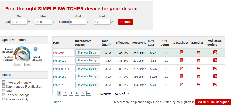
With this in mind, it comes as no surprise that the new SIMPLE SWITCHER product and tool website makes it easier than ever to find the right part using the parameters that you, the designer, care about most- efficiency, size and cost.

 Enter your parameters and click "Update" to instantly view the best SIMPLE SWITCHER solutions for your design. Optimize your results by using the dial and checkboxes on the left.Figure 1. Enter your parameters and click "Update" to instantly view the best SIMPLE SWITCHER solutions for your design. Optimize your results by using the dial and checkboxes on the left.

You know that all of the devices in the search results will be easy to use, because the SIMPLE SWITCHER design team has worked hard over the years so that you and Floyd don’t have to. Innovative design and advances in process technology have enabled the integration of external components as well as the minimization of solution sizes, all in an effort to simplify DC/DC design and get you to market faster. Some examples of said integration, at a glance:

  • Integrated compensation networks take the hassle out of calculating optimal component values to ensure converter stability.
  • Integrated FETs eliminate the need for freewheeling diodes in your design, while improving efficiency and tightening di/dt loops for better EMI performance.
  • Integrated-inductor modules remove what is often the largest and most costly external component, while further tightening di/dt loops and reducing the total BOM count.

The model citizen of the power module community – LMZ31710– requires just three external components to enable a 17V, 10A power supply.

And with the new WEBENCH Interactive Design feature, you are only one click away from previewing a schematic for your design.

 After conducting your part search, click "Preview Design" to open interactive WEBENCH to see schematics, plots, BOM and more - all for your design - without leaving the page.Figure 2.  After conducting your part search, click "Preview Design" to open interactive WEBENCH to see schematics, plots, BOM and more - all for your design - without leaving the page.

Should the design preview tickle your fancy, you can now launch directly into the WEBENCH online design environment. Our hypothetical protagonist, Floyd, will love all of the new time-saving enhancements to TI’s award-winning design tool:

  • The generated schematic can now be edited. Components and/or wiring can be added to the design as needed if the user has unique system requirements.
  • The schematic and simulation test bench can now be exported into the user’s CAD tool. WEBENCH offers the ability to simply download the schematic and simulation files, including SPICE models, which can then be opened and manipulated in CAD software such as Altium, Cadence or TINA-TI.
  • Quickly and simply export the PCB layout. Similar to the schematic and simulation export tools, the thermal simulation layout can downloaded and opened in your CAD tool, saving hours.

A quick perusal of SIMPLESWITCHER.com has done wonders for Floyd. He has numerous potential solutions at his fingertips, his design timeline has been drastically reduced by using WEBENCH design tools, and his nerves have been calmed. Not only will he be able to meet his boss’ deadline, he might even be able to make it to the ice cream social on Friday afternoon.

To try your hand at finding the perfect SIMPLE SWITCHER product for your design, visit simpleswitcher.com and enter your design parameters into the quick search.

Additional resources:

Analog curriculum: A shift towards analog system design

$
0
0

The following is the second blog in the Analog Curriculum blog series. This blog summarizes Dr. KRK Rao’s views on analog curriculum and how it should evolve to meet today’s industry needs.

 Q. As you had mentioned in the previous conversation, we should introduce analog through signal processing applications. Please elaborate why and how.

 A. Analog systems are extensively used in the applied spaces like automotive, medical and motor control electronics. The analog functional building blocks are used to design the front end and the back end subsystems in these application areas for a variety of specifications. There is a greater need in the industry for application engineers who can judiciously use the analog integrated circuits (ICs) to design efficient analog systems rather than IC design engineers who design the analog ICs.

Therefore, engineering students should be first exposed to the applications so that they appreciate the analog processing still required in today’s digitally dominated signal processing systems. For example, front end signal processing functions in communications like amplification, modulation, demodulation, filtering, mixing and frequency multiplication are purely analog.

Students can then be taught about processing functions through the use of basic building blocks like operational amplifiers (op amps), multipliers and comparators, which can be used without device level know-how.

Structuring Analog Courses in UG Curriculum

Q. What is wrong with the traditional approach of introducing analog electronics from device level know-how?

A. With the evolution of devices, analog circuit has migrated from vacuum tubes to Bipolar Junction Transistors [BJTs] to MOSFET, which may be replaced by new devices of the future. The building blocks like op amps, multipliers and comparators will always remain the basic functional blocks of a system design, irrespective of the device technology used for them. Therefore, teaching should be geared towards designing with these building blocks.

Further, op amps have replaced transistors as amplifiers in the front end of the design because of their differential input capability, which improves the signal-to-noise ratio [SNR] and also provides larger dynamic range of operation, which makes them closer to the ideal amplifier. Teaching single ended transistor structures like common emitter, common base and common collector in basic analog courses is no longer relevant.

Q. What should be the focus while teaching analog system design using the building blocks?

A. Current system designs require the use of the intelligent macro model approach to study the input/output behavior of any analog subsystem. This approach starts with the building block and their macro models and uses it to design complex analog systems. It is also important to study the characteristics of the building block by studying the parameters of the macro model. Students must understand the significance of these parameters and their corresponding effect on the system behavior to meet varied application needs. 

To effectively absorb system design using the basic building blocks apart from simulation the lab must expose the students to hands-on exercises as an integral part of the theory course. It must not be isolated from the theory course. It is with this intent we designed Analog System Lab Kit to cover all the basic aspects of signal processing involved in current day analog system design.

Analog System Lab Kit

We will discuss the considerations behind the experiments in Analog System Lab Manual in the following and the last blog in the Analog Curriculum series.

Resources:

European smart grid RF communication in Sub-1 GHz - part 2

$
0
0

Part 1 of this blog series reviews the wM-Bus protocol standard in the 868MHZ ISM band in Europe. Now, let’s have a closer look at the wM-Bus protocol version optimized for the 75 kHz narrowband at 169.400 MHz band, as defined in the European Norm (EN) EN300 220 v2.4.1 standard for tracking, tracing, data acquisition and meter reading applications. The maximum radiated power of +500 mW (or +27 dBm) and the allowed duty cycle of <=10% enable a wide area network (WAN) approach, covering a few kilometers even in dense urban environments. The idea behind it is to have as few as possible but highly-sophisticated data collector (DC) units, each of those serving up to 1000 end nodes (or smart meters) with no repeaters in between. The EN13757-4:2014-2 defines the wM-Bus N-modes Nabcdef and Ng by splitting the 75 kHz total available bandwidth into six narrowband channels of 12.5 kHz each. Four channels (Nabef) can carry data rate of 4.8 kbps while the two (Ncd) others run at 2.4 kbps with 2-GFSK modulation. A higher data rate channel (Ng) has been also defined, utilizing 4-GFSK modulation to achieve data rate of 19.2 kbps and occupying a channel bandwidth of 50 kHz (see Figure 1).


Figure 1 wM-Bus modes N-modes and ETSI 300 220 v2.4.1 relationship

This wM-Bus N-mode has been adopted as the RF communications protocol for residential gas meter deployment in Italy and France as well as for the water meters in France. In N-mode, the highest possible receiver class (Hr) should meet ETSI Category 2 receiver blocking requirements. In practice, designers are well advised to target the significantly more challenging ETSI Category 1 receiver system, due to known interferers such as digital video broadcasting (DVB) or FM radio transmitters which do run on other frequency bands but due to the many kilowatts of RF power, they are causing some interference even in the 169 MHz ISM band.

Now, what actually is ETSI Category 1?

The short answer is that it is the strictest RF receiver specification under EN300 200 v2.4.1 for “Highly reliable SRD communication media; e.g. serving human life inherent systems (may result in a physical risk to a person)…”

One of the most challenging requirements in Category 1 is the adjacent channel rejection/selectivity. This is a measure of how robust the receiver is to an interferer that is only +- 12.5 kHz away. Because of its closeness to the wanted signal, it is not possible to filter this signal out with an external SAW filter. Another very challenging condition to meet is the spurious response rejection that needs to be 60 dB from 0.1% of the RF frequency. At 169 MHz, this is only 169 kHz, so RF transceivers with IF frequency above 85 kHz will get the image frequency above 169 kHz and has to show better than 60 dB rejection.

TI’s high-performance Sub-1 GHz CC1120 RF transceiver family is meeting and exceeding all requirements of the N-mode wM-Bus standard (EN13757-4), including all RF requirements in the Italian and French gas meter specifications. The transceiver fully supports reception of all N-mode telegrams with 16 bits preamble (including the 4-GFSK sub-mode) without packet loss due to its WaveMatch feature.  The extremely fast automatic gain control settling needs only 4 bits; if combined with RX Sniff mode, it keeps the CC1120 sensitivity at the maximum and reduces the average current while searching for a preamble, as shown in TIDC-WMBUS-169MHz. By applying an optimized set of CC1120 register settings, called “best blocking”, an ETSI Category 1 receiver system performance is achievable without needing to add a costly external surface acoustic wave (SAW) filter or LNA component. The CC1120 RF transceiver was the first integrated transceiver in the industry that can achieve ETSI Category 1 compliance without an external SAW filter and is still market leading in RF performance and robustness. More technical information on CC1120 in wM-Bus N-mode is found in the TI Designs reference designs TIDC-WMBUS-169MHz and TIDC-MULTIBAND-WMBUS . The ability to tweak the performance of the CC1120 for “best sensitivity” or “best blocking” with a few register changes enables a flexible wM-Bus N-mode solution, which can dynamically adapt to a changing RF interference in the field.

Besides the RF sub-system itself, TI has also introduced an innovative battery management solution such as the Energy Buffering for Long-Life Battery Applications Reference Design (PMP9753), which eliminates the costly hybrid layer capacitor (HLC) component and enables the use of multiple battery types from different vendors.

Combining the battery management, the N-mode compliant RF system with a complete CIG compliant wM-Bus stack for Italy and advanced ultra-low power metrology (see EVM430-FR6989 for rotation sensing or the ultrasonic TIDM-ULTRASONIC-FLOW-TDC), TI is offering multiple optimized platforms for implementing smart flow meters with 169 MHz RF communication.

The next blog in this series will talk about how a new ultra-low power wireless microcontroller enables next generation single-chip wM-Bus solution for 868 and 433 MHz; stay tuned for an upcoming On the Grid post.

How to get started with current sense amplifiers – part 3

$
0
0

In parts one and two of this series, I discussed concepts related to specifications of current-sense amplifiers and how to use the application requirements to narrow device selection. In this installment, I’ll discuss how the current range helps derive the shunt-resistor value, as well as how the current range and shunt value combined with device performance drive a trade-off between accuracy and power dissipation.

Until the recent release of TI’s INA250 current-sense amplifier (more on this later), the current didn’t actually pass through the current-sense amplifier. Therefore, the current range being measured didn’t directly dictate the device specifications.

For an analog output current-sense amplifier, the maximum current range combined with the full-scale input (maximum differential input voltage) will derive the ideal shunt resistor value, as shown in Equation 1:

                                         (1)

If you look at most current-shunt monitor data sheets, you’ll notice that the maximum differential voltage isn’t specified; rather, a maximum output voltage swing is specified. You’ll want to match this to the full-scale input range of the next link in the signal chain. To maximize performance, you’ll want the maximum-output voltage swing to be greater than the next link’s full-scale input range. Typically, the maximum output swing is a function of the supply voltage supplied to the current-sense amplifier. For example, with the INA282, the output-swing range is defined as 0.4V below the supply voltage to 0.04V above the voltage on the ground pin, as shown on page 6 of the datasheet (Table 1).


Table 1: Electrical characteristics of the INA82 current-sense amplifier

If you use the full-scale input range as the desired output swing of the current-shunt amplifier with maximum current flow, then you can modify the shunt-resistor equation, taking into account the gain (GAMP) of the current-sense amplifier. Equation 2 shows this modification.

                                                  (2)

Let’s look at two examples of how to use this equation. For both examples, we will use the maximum current as 5A and the full-scale input of the next link in the signal chain as 2.5V. Let’s consider using either the INA286 (gain of 100V/V) or INA284 (gain of 500V/V), as shown in Table 2.


Table 2: INA286 and INA284 gain and ideal RSHUNT value with a maximum current of 5A and a full-scale input of 2.5V

The ideal RSHUNT value may not be readily available, so you may have to choose the closest value – which may be is less than ideal. The reason you need to choose a resistor that is of a lesser ohmic value than the ideal is to keep the voltage input to the next link below the full-scale input level.

Using Equation 3, you will also need to verify that the minimum current value creates an output voltage from the current-shunt amplifier that is above the minimum output voltage.

                                          (3)

Looking back at these two examples, you can calculate the minimum current for each solution as 80mA.

The next question is what to do with the fact that I have just calculated multiple options for different combinations of shunt value and amplifier gain. The answer comes down to a trade-off between the desired accuracy of the application versus the power dissipated in the shunt resistor. While I have not delved into accuracy yet, I will cover this in part 4 of this series; briefly, the larger the value of RSHUNT, the higher the accuracy. However, as shown in Figure 3, the higher values of RSHUNT lead to an increase in the power dissipated by the shunt resistor and adds to the overall load of the system.


Table 3: INA286 and INA284 power dissipation and voltage error

You’ll need to look at various current-sense amplifier options for gain and offset voltage and calculate how those options combined with the current range will affect the shunt-resistor value, achievable accuracy and power dissipation.

Most digital-output devices, such as the INA226, specify a full-scale shunt-voltage input range. This simplifies the calculations in many cases because there is not an additional gain stage to trade off against. The shunt value is simply the closest-available value resistor found by dividing the device’s maximum-input voltage by the maximum current.

I mentioned briefly the brand-new INA250 current-sense amplifier. By integrating the shunt resistor, the INA250 can support a maximum current level based on the heat generated by the current flowing through the shunt. Look for more information in future blog posts about how the INA250 is redefining precision current measurement.

In the next installment, I will address the basics of accuracy and how device selection affects accuracy.

Additional resources


SaBLE-x: How this CC2640-based certified module meets three key requirements of IoT

$
0
0

Guest blog post by Dave Burleton, vice president of marketing at LSR

While the exact projections of  “just how big” industry analysts estimate the Internet of Things (IoT) to be, this much is clear:   To meet and exceed those estimated volumes, adding wireless connectivity to a product is a requirement and it must be simple, it must be power-efficient and it simply must work.   More and more, the “things” of the IoT will be items that require a small form factor, long battery life and will need to enable mobile devices to act as a user interface with these products intuitively and reliably.

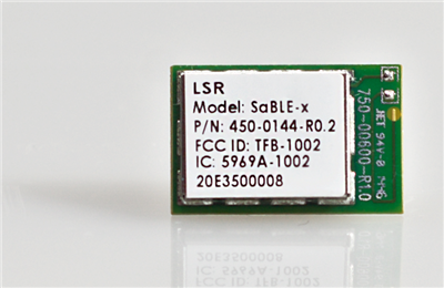
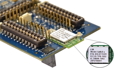
When TI announced the SimpleLink ultra-low power wireless microcontroller (MCU)  family this past February, including the new Bluetooth® Smart CC2640 wireless MCU, it was clear to the product team at LSR (and in short order, to our customers as well) that TI understood the needs for the IoT and set a new bar for Bluetooth Smart solutions moving forward.   LSR, as a platinum partner in the TI Design Network, sought to amplify the design benefits of the CC2640 solution to our customers by placing it within a certified module, the SaBLE-x Bluetooth Smart module. 

So let’s get back to those three key requirements for successful IoT designs, and ask the question:  How does the SaBLE-x offering, powered by TI’s CC2640, achieve them?

Requirement 1:  Must be simple. 

As the IoT brings wireless capabilities into the product lines of more and more companies, development teams who may not have deep experience in Bluetooth communication protocols will need the tools and resources to get the job done and be able to get to market fast.  With a certified modular solution, LSR’s renowned technical support and design tools and TI’s powerful tech resources, customers with any level of wireless expertise can succeed.  A few aspects to highlight:

  • TI’s software & tools:   The CC2640 is supported with TI’s BLE-Stack v2.0, one of the most mature and highly-respected stacks in the industry, the SmartRF™ Studio and full support of integrated development environments (IDE) such as IAR and Code Composer Studio™ IDE
  • LSR’s Serial-to-BLE API:  For many IoT applications, Bluetooth low energy connectivity is being added to a product design with an existing MCU onboard.  LSR’s innovative Serial-to-BLE APIand C-code generation tools provides a simple, straightforward solution for sharing data between host MCU and SaBLE-x module via UART.  The Serial-to-BLE API is just part of LSR’s new Developer Tool Suite PC desktop application.
  • Bluetooth SIG qualification process:  By properly implementing the Bluetooth-qualified BLE stack from TI (QDID # 61713) and the Bluetooth-qualified SaBLE-x module (QDID # 66911) into a product design, additional testing time, expenses, and design risk are all bypassed and the qualification process becomes very streamlined. In addition to the Bluetooth qualification process, the SaBLE-x also provides regulatory certification with FCC, IC, ETSI, Giteki, and C-Tick.  This means dramatically reduced compliance testing and costs for customers’ end products.  You can learn more on TI’s Wiki.

Requirement 2:  Must be power-efficient. 

The “things” of the IoT, like sensors and other ideal Bluetooth Smart applications, will need to live on for long periods of time with minimal intervention from humans.  So battery life becomes paramount.  With the latest generation silicon found on the SimpleLink Bluetooth Smart CC2640 wireless MCU, the SaBLE-x is able to operate at nearly a third of the average power for a 1-second Bluetooth low energy connection interval when compared to our prior-generation Bluetooth Smart module!  By drawing lower currents and having faster, smarter processing on board to maximize the time the module can stay in sleep mode, the SaBLE-x can provide the outstanding battery life many IoT applications call for.

Requirement 3:  It simply must work.  

Any successful product must work when placed in the hands of the end-user and that means reliable connectivity and data-sharing between the “thing” and your mobile device or gateway.   Thanks to the design of the CC2640, the SaBLE-x delivers an impressive 101 dB of link margin, with 5 dBm output power and -96 dBm Rx sensitivity. This improved signal strength provides the additional benefit of improving battery life, as a strong signal connection means the radio does not have to use energy to repeat data transmissions multiple times.  

Hopefully all the industry-leading performance features that TI’s SimpleLink CC2640 wireless MCU offers for IoT applications have been made clear.  For customers who lack the RF expertise in house, or simply need to get to market fast, a certified module based on the CC2640 is likely your best option to take full advantage of it!  If you’re ready for MORE from a Bluetooth Smart module, the time is now as SaBLE-x samples and evaluation kits are available today for your product design.

ABOUT THE AUTHOR:

Dave Burleton is a Vice President at LSR (www.lsr.com), a global leader in wireless product development services and products. He has over 12 years of engineering, marketing, and sales experience in various technology spaces. With leadership roles in product management, strategic marketing, field sales, and sales operations, he approaches new product development from a broad array of perspectives, while maintaining a singular focus on demonstrating value to the customer. He holds a Bachelor of Science degree in Electrical Engineering and Mathematics from the University of Wisconsin – Madison. 

Turn three knobs to power any ultra-low power system

$
0
0

When designing an ultra-low-power system such as a smart watch, low-power sensor node or smart meter, the current required to operate the power supply is critical. This quiescent current (IQ) must be low enough to keep high efficiency even at an ultra-low-power system’s sub-10µA load currents. For example, if your load current is only 1µA, your system will be very inefficient if the power supply powering your load requires 20µA just to operate itself. In other words, you would spend 20µA to deliver just a single microamp! A lower IQ, such as 360 nanoamperes (nA), enables long battery runtimes between charges or a long operational lifetime when running from primary cells.

Besides the IQ and resulting efficiency, such systems have other power-supply design considerations: cost and size, for example. As well, a specific feature may be very useful in a wearable application but useless in a smart meter. With so many different requirements, a one-size-fits-all solution is impossible. There must be trade-offs and optimizations for the three main knobs— efficiency, cost and size— to best fit the variety of ultra-low-power applications.

Wearable applications require both ultra-low power and absolute smallest size and need a truly innovative solution with extremely high levels of integration. What if the power-supply IC integrated all of the components? Since wearables usually have several load switches to disconnect unused subsystems to reduce their leakage current, what if the power supply integrated a load switch as well? Ultra-low-power applications where size is most important would find the TPS82740MicroSiP module most appealing with its complete integration – plus a load switch – in less than 7mm2. However, since a MicroSiP device integrates everything, it clearly has a higher cost than discrete implementations. And because of its very low profile, the inductor used in the MicroSiP has a relatively high DC resistance (DCR), which slightly decreases the efficiency compared to other solutions.

For low-power sensor nodes that need to be small but not necessarily the smallest, where cost is of higher importance, a discrete IC with user-selectable passive components is a more appealing option. An added benefit of this approach is the ability to select a certain inductor to either maximize efficiency or reduce cost. In a remote-sensor node on an oil rig, for example, higher efficiency translates to longer battery run times, which means less service visits from a technician to change the battery. If the sensor node will be more accessible – installed in every ceiling tile in a building, for example – a lower cost may be preferable due to the much larger volume required to equip an entire building.

TI’s TPS62743 and TPS62746 give designers an option of small (10mm2 total size), highly efficient and cost-effective ultra-low-power converters. Figure 1 shows their efficiency of 90% at 10µA of load current. This enables quite a long runtime for battery-powered systems.

Figure 1: The TPS62743/6 offers very high efficiency at very low load currents

Both the TPS62743 and TPS62746 come in wafer-chip-scale packages (WCSPs). Measuring just 1.6mm x 0.8mm, the IC itself is over 75% smaller than its predecessor, the TPS62740. But what if your application isn’t concerned about size or isn’t used to handling such small pitch packages?

In metering and other industrial applications, a traditional quad flat no-lead (QFN) package is preferable. The TPS62740 in its QFN package provides a lower cost than the MicroSiP while maintaining the higher efficiency and inductor flexibility offered by a discrete solution. Having extra pins in a larger package allows a load switch to be integrated as well. Don’t need a load switch? Well, there’s an option here too with the new TPS62745 and its VIN switch. You can read about that feature in my On The Grid blog.

How will you turn the three knobs (efficiency/cost/size) in your ultra-low-power system?

Additional resources:

Summertime showdown: DSPs vs FPGAs

$
0
0

Our fifth episode of our DSP Breaktime video series is up. In this episode we discuss FPGAs, particularly how the 66AK2L06 can replace an FPGA in your system and how the DSP blocks inside an FPGA differ from a dedicated DSP Processor.


We also give our great E2E support forum some love, get you prepped for summer by talking about roller coasters and we reveal what the deal is with the gigantic red cups in our videos.


We’re always looking for what interests you, so send us your questions or topics in the comments section and we’ll address them in future videos. You can also tweet them to us @DSPMark or @EclipseBuzz using the #DSPBreak.


You can also tell us what is your favorite roller coaster or summertime activity as we'd love to know. 


In the meantime, check out our DreamDSP page and enjoy the summer!


DIY with TI: Put on a happy hat

$
0
0

At TI, we celebrate the makers and hobbyists who enjoy creating and innovating on their own time. In our ongoing DIY with TI series, we share their incredible Do It Yourself inventions using TI technology.

TI AvatarNeed a project to prevent boredom and bring a smile to your friends’ faces this summer? Why not fashion your own “smart hat” that lights up, displays messages for your audience, and shows you how well your Facebook and Twitter posts are being received.

The now-famous, do-it-yourself Smart Hat serves as a creative platform for LED lighting technologies and social media messaging. It uses both TI embedded and analog parts, including several of our LED drivers and a SimpleLink™ Wi-Fi® CC3200 wireless MCU, which interacts with the cloud to communicate with others.

“We know that social interaction is very important, and now that we have embedded microcontrollers that can talk through those same social channels, we thought it would be interesting to understand what type of conversations are happening in the cloud,” said Adrian Fernandez, manager of TI’s LaunchPad Development Ecosystem.

While Adrian is generally a happy guy, the open-source Smart Hat displays an ever-changing range of emotions. Green lights mean people are sending happy messages; red lights mean sad messages.

“Using the sentiment analysis tool, we are able to determine whether people were primarily happy that day or sad that day,” Adrian said smiling.

Adrian originally worked with several other TIers to deck out the hat for a Maker Faire in 2014. The hat belongs to Lee Goldberg, an editor at EDN magazine, who loans it to us for events like the “DIY with TI” Showcase Event in May.

Learn more about the hat and how it makes Adrian happy in this video:

(Please visit the site to view this video)

Multiphase DC/DC converters provide low ripple, integrated solution for FPGA power designs

$
0
0

For years, multiphase DC/DC converters have powered multicore processors in servers, mobile phones, tablets and PCs. Today’s modern field-programmable gate arrays (FPGAs) now integrate multicore processors, such as the Xilinx Zynq-7000 series, which features an ARM dual-core Cortex-A9 processor. As multicore processors spread into FPGA, industrial and automotive applications, multiphase DC/DC converter usage continues to grow because of its ability to meet size and thermal constraints.

Multiphase converters have many advantages for powering multicore processors and FPGAs in several applications due to their reduced power losses, low output ripple and fast transient response. To better understand these advantages, let’s review the Xilinx® Zynq®7000 series 5W Small, Efficient, Low-Noise Power Solution reference design (TIDA-00574), which demonstrates how the LP8758-B0 multiphase converter can provide a low-ripple, compact-solution-size, FPGA power solution for industrial designs with effective sequencing (see Figure 1). This reference design can help to improve an engineer’s design cycle by providing a verified design and layout that meets the power requirements for several 5W Zynq FPGAs. The smallest components were chosen to minimize the amount of board space used, while still providing the performance needed to power FPGA rails.

Figure 1: Xilinx Zynq 5W small-solution-size power design

In this design, the LMZ31503, a 3A step-down converter module, supports conversion from a 12V intermediate rail, while offering a small footprint, 2.8mm height and good efficiency over the load range. The LMZ31503 module features an integrated inductor and only one input and output capacitor. The LP8758-B0 is configured to allow multiple output rails to support the Zynq’s power requirements. For this FPGA’s lowest power rails, the design uses a tiny LP5907 low-dropout regulator (LDO)with the market’s smallest 0.65mm-by-0.65mm package, which features an enable pin for sequencing power rails.

The high switching frequency of the LP8758-B0 allows for an overall solution size of ~67mm² with 2010 or 2016 size inductors with 1mm height. This compact design allows for point-of-load capacitor placement very close to the FPGA supply pin to meet the required supply ripple of <30m (see Table 1). The LP8758 evaluation module (EVM) also has the option to add several point-of-load capacitors to optimize for transient performance.

Table 1. Xilinx XC7Z015 transceiver voltage supply requirements.

The multiple output LP8758-B0 offers integrated FETs, low bill of materials and features effective thermal performance because of its efficiency, as shown in Figure 2. The LP8758-B0 has the ability to sequence with multiple EN inputs, meaning an external sequencer such as the LM3880 is not required. At maximum power dissipation, the LP8758 only reaches a maximum temperature of 49°C. Due to the ability to maintain low temperatures, the TIDA-00574 design will be robust and provide reliability to power FPGA’s in space-constrained applications.

Figure 2: See LMZ31503 efficiency, LP8758 efficiency plots for 2.5V, 1.8V, 1.2V, 1.0V outputs over different load current, layout area, and thermal image of design

This design is only one of the many ways to use multiphase DC/DC converters to provide low-ripple, fast transient, and compact board space to power FPGAs or processors. To learn more ways to use small multiphase converters, read my upcoming posts.

Additional resources

How USB Type-C helps make cars as smart as phones

$
0
0

Most of us have become so attached to our phones to stay connected with work, family and friends. However, the place where I feel most unconnected is in my car. My phone is in the passenger seat, gathering new texts, emails, missed calls and social media notifications. At a stoplight, I often grab it to quickly check new notifications. But when I arrive at my destination my phone’s battery is typically low.

I tried all the Bluetooth® products and the 12V phone chargers. I get excited for a while when I buy a new one, but it quickly fails to meet my demands. People complain about my voice quality when I use the speaker in my car, and my phone (which is nearly as capable as a laptop) barely maintains a charge, never coming close to charging with the 500mA current. Not to mention, the audio content is not getting to the car to share on its many capable displays.

When I work with Universal Serial Bus (USB) Type-C, however, I get so excited about how it could change my driving experience that I am actually holding off on trading in my current vehicle until someone realizes the full potential of USB Type-C in cars. USB Type-C would easily provide 15W of charging power (as much as 100W with USB Power Delivery) and 20Gbps of data; even my phone would have to work hard to fill that pipe. It makes my electronics-loving heart excited. I might have to upgrade my phone (or at least its memory); just please don’t tell my wife. On the other hand, please do tell her because this capability would enable all passengers to enjoy their phones’ great capability even more when traveling in my car. It would be even easier to share social media posts with the entire family.

The TUSB320, a device that provides USB Type-C configuration channel logic and port control, could enable this experience and is available today. The device handles all of the USB Type-C channel controller (CC) and mode configuration communication for USB 2.0.

Figure 1: USB 2.0 implementation of Type C

The new TUSB321 can work with the HD3SS3212 device to enable a full USB 3.1 solution, thus using the full data transfer benefits of the USB Type-C connector.

Figure 2: USB 3.0 implementation of Type C

 TUSB320, TUSB321, HD3SS3212 and HD3SS460 are commercially available and Q100 qualification is possible on most devices. It’s so exciting to think that my next car might have these capabilities.

Are you ready to utilize your phone capability while in the car and arrive with a full charge? USB Type-C can make this a reality in your next vehicle. If you have any questions about how TI products are bringing this experience to life, please leave a comment below.

Six ways to sense current and how to decide which to use

$
0
0

High-precision current sensing is key to improve efficiency of closed-loop control systems, i.e. motor drives. In this blog, I summarize the pros and cons of different approaches to isolated current sensing and list some typical applications in which they’re used.

Shunt resistors are used in wide range of industrial applications and offer relatively high accuracy at low temperature drift. However, their use is limited by the power dissipation caused by their own resistance value. In applications with high common-mode voltages, shunt resistors require isolated amplifiers such as the AMC1200 or, for the highest-performing systems, an isolated delta-sigma modulator like the AMC1304L05. This device offers a low input voltage range of ±50mV allowing you to use smaller resistance shunts without compromising performance. 

Figure 1: AMC1304L05- Effective number of bits versus oversampling ratio


Rogowski coils measure alternating current (AC) only and are wrapped around a conductor that distributes the current to be sensed. They deliver a voltage proportional to the rate of change of the AC current and therefore require an integrator before being processed using an analog-to-digital converter (ADC).

Rogowski coils are suitable for retrofitting applications because the coil can be mounted around the conductor without interrupting the current flow. They don’t use a metal core, so the mechanical tolerances of the positioning both influence and limit the achievable accuracy. For the same reason, they don’t saturate and are thus used in high-current applications. Their low inductance allows usage in systems with high slew rates.

In current transformers (CTs), the primary AC current generates a field in a magnetic core. This magnetic field induces a proportional current in the secondary winding. A burden resistor is required to convert the current to a voltage signal for further processing in an ADC.

The accuracy of CTs depends on the mechanical tolerances of the setup, burden accuracy and temperature drift of the magnetic core. The saturation level of the magnetic core limits the dynamic range of a CT. On the other hand, dedicated design allows you to tailor the CT for a certain use case. CTs are widely used for sensing currents in power grids.

Magnetoresistive sensors change their resistance with the presence of magnetic field, direct current (DC) or AC. Magnetoresistive sensors are small in size and are typically used for position and angle sensing. They are cost-effective alternatives for low-current applications that don’t require high accuracy.

Depending on the material used, you can choose from two types of magnetoresistive sensors:

  • Anisotropic magnetoresistance(AMR) sensors use ferromagnetic materials in which a magnetic field influences the electrical resistance. The resistance variation is very small; therefore, Wheatstone bridges are often used to sense it.
  • Giant magnetoresistance (GMR) sensors rely on a significantly higher impact of the magnetic field on the resistance of a structure built of alternating ferromagnetic and nonmagnetic layers. There is no free lunch, though – compared to AMR sensors, the production process is more complex and expensive.

Hall-effect sensors deliver a voltage signal proportional to an AC or DC magnetic field. They are inherently noisy, and the voltage level is highly temperature-dependent. You can address both limitations using clever excitation approaches like those used in the DRV411 sensor signal-conditioning integrated circuit (IC).

Hall sensors can be used in open-loop applications that don’t require high accuracy levels. For better accuracy, closed-loop approaches are best; these include the Hall sensor, a magnetic core with compensation winding, and a signal-conditioning circuit that is usually in the form of a complete module. Closed-loop modules are available for wide range of accuracy, current and cost levels. Other examples of Hall-effect sensors include the DRV5000 family.

Fluxgate sensors deliver the highest level of sensitivity, widest dynamic range, and lowest noise and temperature-drift performance compared to other current-sensing methods. The design of an external fluxgate sensor is complex and requires low mechanical tolerances; only a few manufacturers worldwide offer fluxgate-sensor modules. TI recently announced the DRV421, the industry’s first fully integrated fluxgate sensor with all of the required signal-conditioning functions for closed-loop DC and AC applications. With a magnetic core and a compensation coil, this solution allows easy manufacturing of high-accuracy and low-level (leakage) current modules.

Table 1 compares all of the methods described in this post.

Table 1: Comparison of current sensing methods

Stay tuned next month for more details on shunt-based current sensing.

Additional resources:


Power Tips: Designing an LLC resonant half-bridge power converter

$
0
0

Unlike traditional pulse-width modulation (PWM) power converters, resonant converter output voltages are regulated by frequency modulation. Therefore, the design methodology of a resonant converter will be different from a PWM converter.

Among various types of resonant converters, the LLC series resonant converter (LLC-SRC) in Figure 1 attracts interest because of its better output regulation, lower circulating current and lower circuit cost.

Figure 1: LLC-SRC with AC input/output voltage

The series resonant characteristics allow the switching network in a DC/DC LLC-SRC, such as that shown in Figure 2, to have very wide region of zero-voltage switching (ZVS); hence, the LLC-SRC can easily achieve over 94% efficiency in front-end power-supply applications and operate at a high switching frequency.

Figure 2: LLC resonant half-bridge converter

Similar to the design process for PWM converters, the first step when designing an LLC-SRC is to select the desired operation frequency at full load. The remaining steps are different, because there is no duty-cycle factor in a resonant converter. The duty cycle remains unchanged in an LLC-SRC and is ideally 50%. Figure 3 shows a design flow chart for an LLC-SRC from TI Power Supply Design Seminar topic “Designing an LLC Resonant Half-Bridge Power Converter.”


Figure 3: LLC resonant half-bridge converter design flow chart

Notice that Mg is the DC voltage gain, Ln is the ratio of Lm and Lr, and the quality factor is defined as Equation 1:


Also, fn is the normalized frequency defined as fn = fsw/fo, where

The gain curves in both the Mg/Qe and Mg/fn charts are derived from the LLC resonant tank shown in Figure 1, which is also a linearized circuit of a LLC resonant half-bridge converter.

Figure 3 provides a simple circuit parameter selection process of an LLC resonant half-bridge converter. By checking the fn_min, fn_max locations on the gain curves, you will be able to design a high-efficiency LLC resonant half-bridge converter with ZVS on the switching network under all input conditions.

When designing a LLC resonant half-bridge converter, keep in mind that:

  • fn_min needs to be above the ridges of the gain curves in the Mg/fn chart at all times. This is to make sure that the MOSFETs maintain ZVS.
  • LLC-SRC efficiency can only be optimized at one operation point. When fsw = fo, the series Lr and Cr become zero impedance (Figure 4); the converter has best efficiency at that point. You will need to decide the line/load condition that you want to optimize and make sure that your switching frequency is at resonant frequency at that condition.

Figure 4: LLC-SRC with AC input/output voltage when fsw = fo

Additional resources


Inductive sensing: How to sense spring compression

$
0
0

While most inductive-sensing applications use either printed circuit board (PCB) coils or wire-wound inductors as the sensor, inductance-to-digital converters (LDCs) can use almost any inductor as a sensor – even a spring. Springs are useful as sensors because the spring’s inductance varies directly with changes in length or other physical changes. Figure 1 shows how to connect a spring to an LDC.

Figure 1: Spring used as a sensor by an LDC

To evaluate using a spring as a sensor, I used the LDC1612EVM evaluation module to measure the inductance of a spring as I extended the spring across a range of lengths. To do this, I first removed the on-board sensor from the EVM and replaced it with a spring. The spring was made of 0.7mm-thick steel, had 46 turns and a diameter of 7.3mm. Figure 2 shows the spring that I connected to the EVM.


Figure 2: Spring setup

The inductance of my spring is too low to be used as a sensor for the LDC1612 on its own, so I added a 2.2μH fixed wire-wound surface-mount device (SMD) inductor in series. (For details on how to use a series inductor to increase sensor impedance, see my blog post “How to use a tiny 2mm PCB inductor as a sensor.”) With a 1nF sensor capacitor, the oscillation frequency was 2.5MHz. Figure 3 shows the sensor components that I used.


Figure 3: Sensor components

I stretched the spring from 50mm to 100mm in 5mm increments and measured LDC1612 output data at each step. From the data, I calculated the sensor inductance using Equation 1:

                                (1)

where

and fref = reference clock (40MHz on the LDC1612 EVM).

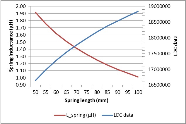
Figure 4 shows the data and spring inductance after subtracting the 2.2μH series inductor.

Figure 4: LDC1612 data and spring inductance versus spring length

The data samples that I collected when extending the spring from 50mm to 100mm in 5mm steps are monotonic and can be used to precisely determine the length of the spring. During this spring-compression range, the inductance decreases from 1.92μH (LDC output 16,644,000) to 1.01μH (LDC output 18,840,000). Thus, over this range, stretching the spring by 1μm results in a 44-codes increment in the LDC1612 data output on average.

This data shows that you can use inductive sensing to directly measure the inductance shift that results from compressing a spring, and that springs can serve as an alternative sensor to PCB coils and wire-wound inductors.

Additional resources

Simple circuit drives TECs

$
0
0

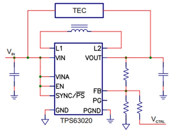
Figure 1: PMP9759 is a simple circuit which drives TECs

In optical networking modules and other communications systems, you may have to precisely control the temperature of a certain component. Lasers, for example, need a specific temperature in order to emit a certain wavelength of light. A thermoelectric cooler (TEC), shown in Figure 1, is a common device used to either heat or cool a component in such systems.

Using a single element like a TEC for heating or cooling requires the power supply supplying the TEC to source and sink output current. Sourcing current through the TEC cools, while sinking current from the TEC heats. Using a TEC requires a bidirectional current flow, but only certain power supplies are configurable to both source and sink current. Even fewer power supplies are capable of sourcing and sinking the higher currents necessary for larger TECs. TI Design reference design PMP9759 details the implementation of such a circuit, which is capable of sourcing up to 1.5A though the TEC.

In PMP9759, the TPS63020buck-boost converter is operated in forced pulse-width modulation (PWM) mode to achieve the ability to both source and sink. The TPS63020 is a good fit for optical networking applications, which are frequently powered from 3.3V. As well, it has a wide output voltage range of 1.2V to 5.5V. Such a wide range allows the most current flow through the TEC because it generates higher voltages across the TEC. Attaching the TEC from the input voltage to the output voltage instead of from the output voltage to ground enables a bidirectional current flow. Current flows in one direction to heat and the other to cool.

The onboard microcontroller (MCU) measures the temperature of the TEC and outputs either an analog or digital PWM signal to adjust the current sourced or sunk by the TPS63020. Sending this signal into the feedback pin of the TPS63020 adjusts the TEC current. Adjusting the current adjusts the temperature of the TEC, which is then fed back to the MCU, resulting in a closed-loop system that properly controls temperature. Figure 2 shows the complete circuit.

In what systems do you need bidirectional current capability?

Figure 2: The TPS63020 simply implemented as a TEC driver

Call for Submissions: International Symposium on Emerging and Industrial TI DLP® Technology Applications

$
0
0
We’re searching for the best and brightest to tell us how TI DLP ® Technology is helping advance new markets. The 10th International Symposium on Emerging and Industrial TI DLP ® Technology Applications , which will be held on October...(read more)

Motor Drive forum Top FAQs Part 2: How to estimate motor regeneration and VM pumping

$
0
0

Motor regeneration is a common problem that occurs in motor-drive systems. Many designers have to select a motor supply voltage (VM) rating of twice the nominal level, which adds to the system cost. Fortunately, if you can first understand the pumping details, you can understand the necessary VM margin. In the first post in this series on frequently asked questions, Nicholas Oborny provided advice on how to read a motor driver datasheet. Today, I’ll continue the conversation by introducing a method for estimating the pumping level.

VM pumping waveform

Figure 1 shows a typical VM pumping waveform caused by regeneration during a deceleration process. When the input PWM (pulse-width modulation) duty changed from 99% to 70%, the VM voltage was pumping from 24V to 32V. (Tested on TI motor driver device DRV8840, a 5A Brushed DC Motor Driver.)


Figure 1: Regeneration and VM pumping


Pumping mechanism

We need some DC/DC power management background here to understand the pumping mechanism. So, let’s look at how a typical buck-boost circuit works; see Figure 2. What’s interesting is that during PWM, driving a motor with an H bridge, you have the buck and boost process together. As shown in Figure 3, during the PWM’s driving time, it’s a typical buck circuit. In Figure 4, the back electromotive force (EMF) is acting as the boost source during the PWM’s off time.

VM Pumping

Figure 2: Buck and boost circuits


buck topology 

Figure 3: Buck topology


boost topology

Figure 4: Boost topology


The running model of the brushed DC motor can be shown as equation (1).

In normal driving conditions with a PWM duty cycle = D, the motor will run at a speed driven by a voltage VDRV as shown in equation (2).

Based on (1), we should have

The boost effect will give the VBST as

From (2), (3), (4), we can get

So, there is no VM pumping in a normal running condition.

When the PWM duty cycle is reduced from D1 to D2, just before the reducing point, we have

Just after the reducing of duty, the speed of the motor can’t change suddenly, so the VBST is based on the new duty cycle D2 as

From (6), (7), we can get

When K*D1/D2 > 1, we get

VBST will be higher than VVM and causing a pumping effect. Assuming that K is close to 1, any time you reduce the duty cycle with D2 < D1, VM pumping will occur. For example, if you go from 100% to 50%, VBST = 2*VM. And if you go from 90% to 30%, there will be 3x higher pumping voltage seen from VM.

Pumping tests

In practice, VM pumping may not be seen as high as estimated by the above equation (8), because the power supply and VM caps will have sinking ability which helps to reduce the pumping level. To verify the estimating method, we add a diode Ts1 from the power supply to the VM, as shown in Figure 5, trying to get the pure pumping effect without power supply sinking.


Pumping voltage tests 

Figure 5: Pumping voltage tests


Table 1 and Figure 6 show the test results. (Note: Some pumping voltage is over the VM spec of the DRV8840 datasheet; this is for test only. The device is never recommended to be used in over-spec conditions.)

Table 1: Tested result and calculated result


Figure 6: Bar plot of results


 pumping when PWM reduces from 100% to 50%

Figure 7: VM pumping when PWM reduces from 100% to 50% (with Ts1 on Figure 5)


Reducing voltage pumping

There are two ways to control VM pumping:

  • Use fast decay. With DRV8840 in fast decay mode, the boost topology shown in Figure4 is no longer present. The back EMF will always be less than the VM voltage, and VM pumping will not occur at all. It will take a longer time to achieve the targeted speed, as shown in figure 8.

VM pumping

Figure 8: No VM pumping with fast decay

  • Use a transient voltage suppressor (TVS) to clamp the VM pumping. If you choose the TVS with clamping voltage a little higher than the nominal VM rating and place it as Ts2, shown in Figure 5, it will clamp the VM pumping (see Figure 9). I used a 27V TVS and the VM pumping was effectively clamped at 29.6V. The TVS also functioned as dynamic braking so that the motor has a quick deceleration process.


Figure 9


Summary

In a motor deceleration process, VM pumping actually shows the kinetic energy transferring into electrical energy. Consider the below factors:

  • The boost topology is a key factor as to why the back EMF can force current back to the VM supply, even when VBEMF< VVM.Fast decay will not cause VM pumping during the deceleration section, but it will take a longer time for the motor to slow down.
  • A TVS clamping method or other dynamic braking method can be a good way to reduce VM pumping while keeping the fast deceleration rate. 

Additional resources


Viewing all 4543 articles
Browse latest View live


<script src="https://jsc.adskeeper.com/r/s/rssing.com.1596347.js" async> </script>